Positive Voltage Regulators with Builtin Voltage Detect Functions
Series
373
3
General Description
Features
Applications
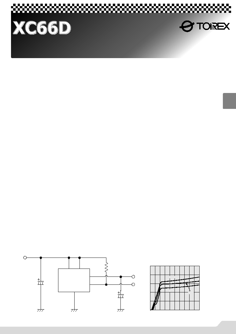
Typical Application Circuit
Typical Performance
Characteristic
The XC66D series consists of a voltage detector and voltage regulator
built into the one chip and is, essentially, a voltage regulator with voltage
detect capabilities.
Low power consumption and high accuracy is achieved through CMOS
and laser trimming technologies.
The detector features an output driver, hysteresis circuit, comparator and
extremely accurate standard voltage.
The regulator features an error amplification circuit, output driver with
current limiter functions, minimal input-output voltage differential and
similary accurate standard voltage.
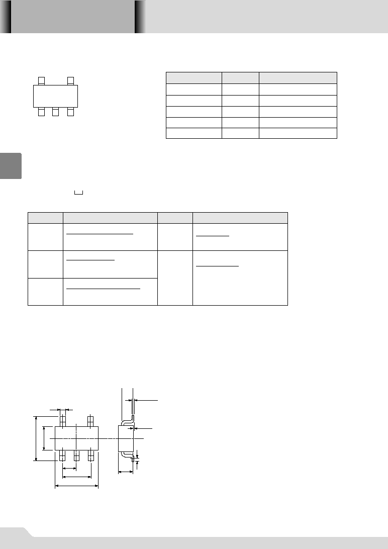
SOT-25 (150mW) package is available.
GBattery use
GBattery life & charge detection
GMemory battery back-up circuits
GMicroprocessor reset circuitry
GPower failure detection
GVoltage Sources Reference
GCameras, Video Cameras
GVarious Portable Devices
NCMOS
NMaximum Output Current : 100mA(V
OUT
=5.0V)
NHighly Accurate Output Voltage : ±2%
NOutput Voltage Range
: 2.0V~ 6.0V
NHighly Accurate Voltage Detection : ±2%
NNo Load Supply Current : 3.2µA(5.0V)
NSOT-25 Package
100k
V
OUT
V
IN
V
SS
VD
IN
VD
OUT
1
µF
1
µF
Tantalum
Tantalum
0
2
1
3
4
5
0
1
2
3
4
5
6
7
8
9
10
Input Voltage:V
IN
, VD
IN
V
XC66DN1922
Topr80
25
-30
V
IN
VD
IN
Supply Current:Iss
µ
A
Maximum Output Current
: 100mA (Within max.
continuous total power
dissipation, V
OUT
=5.0V)
Output Voltage Range
: 2.0V ~ 6.0V (0.1V steps,
Standard 5.0V)
Highly Accurate Output Voltage : Fixed voltage accuracy ±2%
Output Voltage Temperature Characteristics
: Typ. ±100ppm/°C
Detect Voltage Range
: 1.8V ~ 6.0V (0.1V steps)
Highly Accurate Detect Voltage : Fixed voltage accuracy ±2%
Low Power Consumption
: Typ. 3.2
µA (V
OUT
= 5.0V)
Detect Voltage Temperature Characteristics
: Typ. ±100ppm/°C
Detect Voltage Output Configuration
: N-ch open drain
CMOS (High level =V
OUT
)
Input Stability
: Typ. 0.1%/V
Ultra Small Packages
: SOT- 25 (150mW) mini-mold
03S_11XC66D 02.9.12 3:09 PM 373
w Represents the decimal number of the Detect Voltage and
the Off-set of the Output Voltage
DESIGNATOR
DETECT VOLTAGE
OFF-SET OF THE
OUTPUT VOLTAGE
VOLTAGEVDESIGNATOR VOLTAGEV
X.0
0V
X.1
X.2
X.3
X.4
5V
X.5
X.6
X.7
X.8
X.9
X.0
X.1
X.2
X.3
X.4
X.5
X.6
X.7
X.8
X.9
5
6
7
8
9
H
K
L
M
F
0
1
2
3
4
B
C
D
E
A
e Represents the Output Voltage
N
U
T
Z
S
Y
R
X
P
V
A
F
E
M
D
L
C
K
B
H
DESIGNATOR
DETECT VOLTAGE
INTEGER OF THE
OUTPUT VOLTAGE
VOLTAGEVDESIGNATOR VOLTAGEV
X.0
0V
+
Off-set
X.1
X.2
X.3
X.4
4V
+
Off-set
X.5
X.6
X.7
X.8
X.9
X.0
X.1
X.2
X.3
X.4
X.5
X.6
X.7
X.8
X.9
5
6
7
8
9
0
1
2
3
4
3V
+
Off-set
X.0
X.1
X.2
X.3
X.4
X.5
X.6
X.7
X.8
X.9
2V
+
Off-set
X.0
X.1
X.2
X.3
X.4
X.5
X.6
X.7
X.8
X.9
V
X
Y
Z
U
P
R
S
T
N
1V
+
Off-set
X.0
X.1
X.2
X.3
X.4
X.5
X.6
X.7
X.8
X.9
H
K
L
M
F
B
C
D
E
A
r Denotes the production lot number
0 to 9, A to Z repeated(G.I.J.O.Q.W excepted)
* Italic type : Character inversion
Marking
SOT-25
(TOP VIEW)
q w e r
DESIGNATOR
DETECT VOLTAGE
PRODUCT SERIES TYPE
A
F
VOLTAGEVDESIGNATOR VOLTAGEV
0.X
N-ch
XC66DN Series
B
H
1.X
C
K
2.X
D
L
3.X
E
M
4.X
N
U
0.X
T
Z
4.X
S
Y
3.X
R
X
2.X
CMOS
High level V
IN
XC66DD Series
P
V
1.X
A
F
0.X
E
M
4.X
D
L
3.X
C
K
2.X
CMOS
High level V
OUT
XC66DC Series
B
H
1.X
5.X
6.X
7.X
8.X
9.X
5.X
9.X
8.X
7.X
6.X
5.X
9.X
8.X
7.X
6.X
q Represents the Product Series, Type, and the integer of the Detect
Voltage
XC66D
Series
375
3
03S_11XC66D 02.9.12 3:09 PM 375
XC66D
Series
376
3
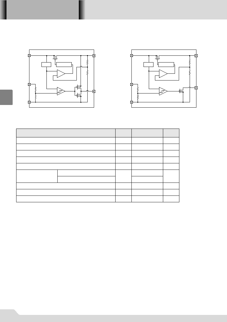
Block Diagram
(1) XC66DC CMOS output (High level =V
OUT
)
(2) XC66DN N-ch open drain
Voltage Limiter
Vref
V
IN
V
SS
VD
IN
V
OUT
VD
OUT
+
-
+
-
Voltage Limiter
Vref
V
IN
V
SS
VD
IN
V
OUT
VD
OUT
+
-
+
-
Absolute Maximum Ratings
Ta=25
°C
Please ensure that {(V
IN
-V
OUT
) x I
OUT
} + {ID
OUT
x VD
OUT
} + {V
IN
x I
SS
} does not exceed the stated Pd values.
Note:
PARAMETER
Regulator Input Voltage
Regulator Output Voltage
Regulator Output Current
N-ch open drain output
Detector
Output Voltage
CMOS output (High level =V
OUT
)
Continuous Total Power Dissipation
Operating Ambient Temperature
RATINGS
V
SS
-0.3 ~ 12
V
SS
-0.3 ~ V
IN
+0.3
150
V
SS
-0.3 ~ 12
V
SS
-0.3 ~ V
IN
+0.3
150
-30 ~ +80
UNITS
V
V
mA
V
mW
°C
SYMBOL
V
IN
V
OUT
I
OUT
Detector Output Current
Detector Input Voltage
50
V
SS
-0.3 ~ 12
mA
V
ID
OUT
VD
IN
VD
OUT
Pd
Topr
Storage Temperature
-40 ~ +125
°C
T
stg
03S_11XC66D 02.9.12 3:09 PM 376
XC66D
Series
377
3
Electrical Characteristics
Ta=25
°C
V
DF
=1.8V ~ 6.0V, V
OUT
(T)
(Note1)
=5V
PARAMETER
MIN
(V
DF
)
x 0.98
1.5
10.0
-
TYP
V
DF
MAX
(V
DF
)
x 1.02
UNITS
V
mA
V
CIRCUIT
1
(V
DF
)
x 0.02
(V
DF
)
x 0.05
(V
DF
)
x 0.08
V
1
4.9
5
5.1
V
4
100
-
-
mA
4
-
20
80
mV
4
-
260
520
mV
4
-
0.1
0.3
%/V
4
-
±100
-
ppm/
°C
4
2
-
-
0.4
1.0
µA
3
-
V
-
-
-
3.2
10.0
8.6
mA
5
±100
-
-
ppm/
°C
1
-30
°C Topr 80°C
Detect Voltage
Temp. Characteristics
DETECTOR
REGULATOR
V
OUT
Topr
·
V
OUT
V
OUT
Topr
·
V
DF
V
OUT
V
IN
·
V
OUT
Output Voltage
Temp. Characteristics
V
OUT
N-ch
V
DS
=0.5V
V
SS
=1.5V
=2.0V
=3.0V
=4.0V
=5.0V
0.3
3.0
5.0
6.0
7.0
2.2
7.7
10.1
11.5
10.3
-
-
-
-
-
P-ch
V
DS
=0.9V
V
IN
=VD
IN
=V
OUT
=8V
(CMOS)
-
-5
-2
6
1. V
OUT
(T) : User specified output voltage.
2. V
OUT
(E) : Effective output voltage.
(i.e. the output voltage when a stable (V
OUT
(T) + 1.0V) is provided, while maintaining a certain I
OUT
value.)
3. Vdif
: Vdif = {V
IN
1 - V
OUT
1}
V
OUT
1
: The voltage equal to 98% of the output voltage whenever a stable (V
OUT
(T) +1.0V) is provided at I
OUT
.
V
IN
1
: The input voltage when the output is equal to V
OUT
(E) x 98%.
Note:
Detect Voltage
Output Current
Hysteresis Range
Output Voltage
Maximum Output
Current
Load Stability
Input - Output
Voltage Differential
Input Stability
Operating Voltage
VD
IN
Input Current
Input Voltage
Supply Current
SYMBOL
CONDITIONS
V
DF
V
IN
= VD
IN
ID
OUT
V
HYS
V
IN
= VD
IN
V
OUT
(E)
(Note2)
I
OUT
=10mA
V
IN
= V
OUT
(T) + 1V
I
OUT
max
V
IN
= V
OUT
(T) + 1V
V
OUT
(E)
V
OUT
(T) x0.9
V
IN
= V
OUT
(T) + 1V
1mA
I
OUT
80mA
Vdif
(Note3)
I
OUT
=60mA
I
OUT
=10mA
V
OUT
(T) + 1V
V
IN
10V
I
OUT
=10mA
-30
°C Topr 80°C
V
IN
ID
IN
VD
IN
=10V
V
IN
I
SS
V
IN
= V
OUT
(T) +1V
03S_11XC66D 02.9.12 3:09 PM 377