
CMOS Logic
1003
13
General Description
Features
Applications
The XC74ULU04A is a CMOS Inverter, manufactured using silicon gate
CMOS fabrication.
CMOS low power circuit operation makes high speed LS-TTL operations
achievable.
The internal circuit is composed of a single stage inverter, so can be
used in the crystal oscillator.
As the XC74ULU04A is integrated into mini molded, SSOT-25 and SOT-
25 packages, high density mounting is possible.
High Speed Operation
: tpd=2.3ns TYP
Operating Voltage Range : 2V~5.5V
Low Power Consumption: 1
µA (max)
Ultra Small Package
: SSOT-25 and SOT-25
GCrystal Oscillators
GPalmtops
GDigital Equipment
NCMOS Inverter
NUnbuffered Type
NHigh Speed Operation
: tpd=2.3ns TYP
NOperating Voltage Range : 2V~5.5V
NLow Power Consumption : 1µA (max)
Pin Configuration
Function
Absolute Maximum Ratings
H=High level, L=Low level
INPUT
A
Y
H
L
L
H
OUTPUT
Ta=-40
∞C~85∞C
PARAMETER
RATINGS
UNITS
SYMBOL
Power Supply Voltage
-0.5 ~ +6.0
V
V
CC
Input Voltage
-0.5 ~ +6.0
V
V
IN
Output Voltage
-0.5 ~ V
CC
+0.5
V
V
OUT
Input Diode Current
-20
mA
I
IK
Output Diode Current
±20
mA
I
OK
Output Current
±25
mA
I
OUT
V
CC
,GND Current
±50
mA
I
CC
, I
GND
Continuous Total
Power Dissipation (Ta=55
∞C)
150
mW
Pd
Storage Temperature
-65 ~ +150
∞C
Tstg
Note: Voltage is all Ground standardized.
2
1
3
4
5
NC
A
GND
Vcc
Y
SSOT-25/SOT-25
TOP VIEW
13S_39XC74ULU04AN 02.09.12 16:14 1003
XC74ULU04A
1004
13
DC Electrical Characteristics
Switching Electrical Characteristics
MIN TYP MAX MIN MAX
1.7
V
CC
(V)
2.0
-
-
1.7
-
2.4
3.0
-
-
2.4
-
4.4
5.5
-
-
4.4
-
-
2.0
-
0.3
-
0.3
-
3.0
-
0.6
-
0.6
-
5.5
-
1.1
-
1.1
V
IH
V
Input Voltage
V
IL
V
1.8
2.0
2.0
-
1.8
-
2.7
I
OH
=-50
µA
3.0
3.0
-
2.7
-
4.0
4.5
V
IN
=V
IL
4.5
-
4.0
-
2.58
3.0
-
-
2.48
-
3.94
I
OH
=-4mA
I
OH
=-8mA
4.5
-
-
3.80
-
V
OH
V
-
2.0
-
0.2
-
0.2
-
I
OL
=50
µA
3.0
-
0.3
-
0.3
-
4.5
V
IN
=V
IH
-
0.5
-
0.5
-
3.0
-
0.36
-
0.44
-
I
OL
=4mA
I
OL
=8mA
4.5
-
0.36
-
0.44
-
V
IN
=V
CC
or GND
Input Current
V
IN
=V
CC
or GND, I
OUT
=0
µA
5.5
Quiescent Supply Current
I
IN
5.5
I
CC
-
1.0
-
10.0
-0.1
-
0.1
-1.0
1.0
V
OL
V
µA
Output Voltage
UNITS
Ta=-40~85
∞C
Ta=25
∞C
CONDITIONS
PARAMETER
SYMBOL
MIN TYP MAX MIN MAX
C
L
-
15pF
2.8
8.9
1.0
10.5
-
tPLH
2.4
5.5
1.0
6.5
-
50pF
4.5
11.4
1.0
13
-
15pF
2.7
8.9
1.0
10.5
-
tPHL
2.2
5.5
1.0
6.5
-
50pF
ns
ns
ns
ns
4.2
11.4
1.0
13
Input Capacitance
C
IN
-
V
CC
(V)
3.3
5.0
3.3
-
3.6
7
1.0
8
5.0
3.3
5.0
3.3
-
3.5
7
1.0
8
5.0
5.0
-
2
10
-
10
pF
Power Dissipation Capacitance
Cpd
No Load, f=1MHz
V
IN
=V
CC
or GND
-
16
-
-
-
pF
Propagation Delay Time
UNITS
Ta=-40~85
∞C
Ta=25
∞C
CONDITIONS
PARAMETER
SYMBOL
tr=tf=3ns
Recommended Operating Conditions
V
CC
V
OUT
Topr
V
V
∞C
V
IN
V
0 ~ 100
tr, tf
Supply Voltage
Output Voltage
Operating Temperature
Input Voltage
Input Rise and Fall Time
2 ~ 5.5
0 ~ V
CC
-40 ~ +85
0 ~ 5.5
I
OH
I
OL
Output Current
mA
-4
4
8
-8
0 ~ 20
3.3
3.0
3.0
4.5
4.5
5.0
ns
UNITS
CONDITIONS
PARAMETER
SYMBOL
-
-
-
-
V
CC
(V)
13S_39XC74ULU04AN 02.09.12 16:14 1004
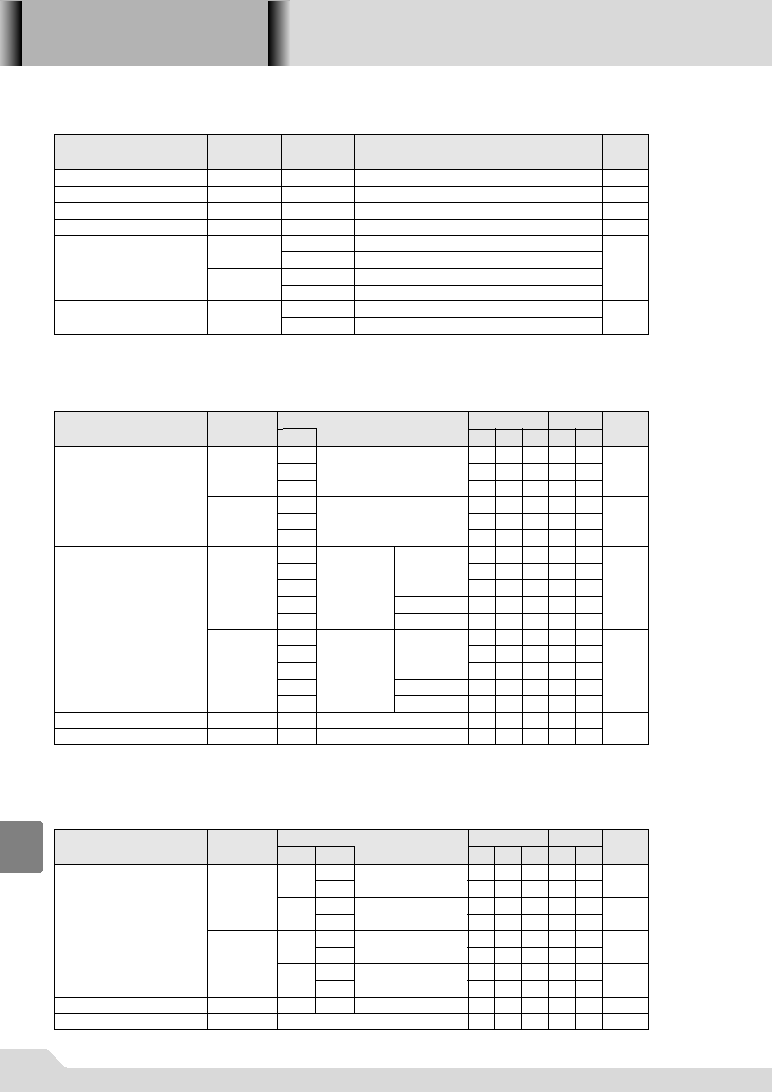
Waveforms
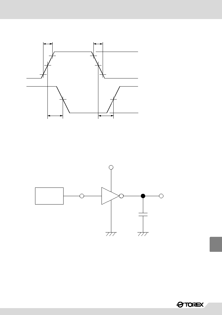
Typical Application Circuit
tr
tf
10
50
50
t
PLH
t
PHL
90
90
50
50
GND
V
OH
V
cc
V
OL
10
Input
Output
PRR1MHz
duty cycle 50%
trtf3ns
Note: Open output when measuring supply current
Z
OUT
50
Pulse
Generator
Vcc
C
L
Output
Input
XC74ULU04A
1005
13
13S_39XC74ULU04AN 02.09.12 16:14 1005