CMOS Logic
907
13
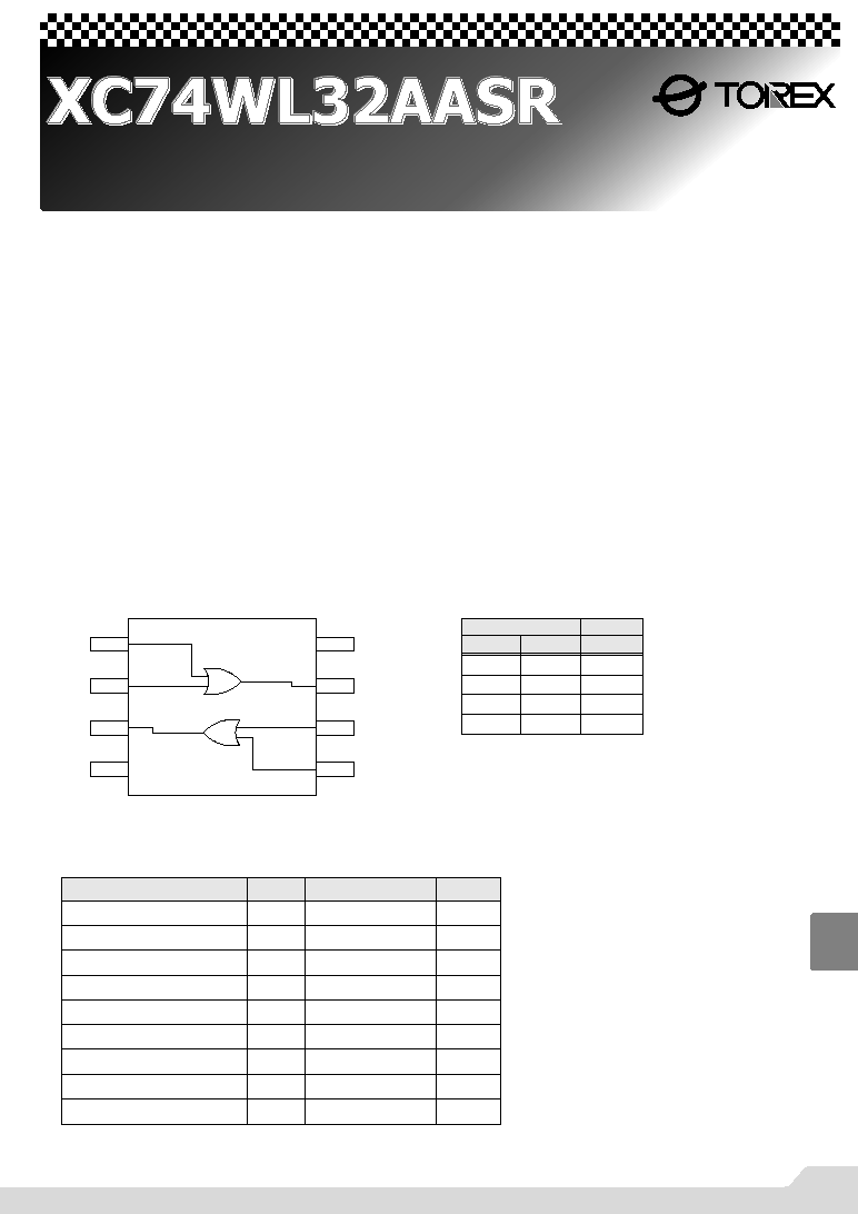
XC74WL32AASR is dual 2-input OR gate manufactured using silicon
gate CMOS processes. The small quiescent current, which is one of the
features of the CMOS logic, gives way to high speed operations which
enables LS-TTL.
With wave forming buffers connected internally, stabilized output can be
achieved as the series offers high noise immunity.
As the series is integrated into a mini molded, MSOP-8B package, high
density mounting is possible.
Description
High Speed Operations
: tpd = 3.8ns TYP (V
CC
=5V)
Operating Voltage Range : 2V ~ 5.5V
Low Power Consumption: 1
µA (max)
Small Package
: MSOP-8B
GPalmtops
GDigital Equipment
Features
Applications
NCMOS Logic
NOperating Voltage Range : 2V ~ 5.5V
NHigh Speed Operations : tpd = 3.8ns TYP
NLow Power Consumption : 1µA (max)
NMSOP-8B Package
Pin Configuration
Functions
Absolute Maximum Ratings
V
CC
2B
1A
1B
2Y
GND
1Y
2A
1
2
3
4
5
6
7
8
MSOP-8B
TOP VIEW
H = High Level
L = Low Level
INPUT
OUTPUT
B
A
H
H
H
L
L
H
Y
H
H
H
L
L
L
PARAMETER
Power Supply Voltage
SYMBOL
RATINGS
UNITS
-20
Input Voltage
Output Voltage
Input Diode Current
Output Diode Current
V
CC
, GND Current
V
CC
V
IN
V
OUT
I
IK
I
OK
I
CC
, I
GND
-0.5+6.0
-0.5+6.0
-0.5V
CC
0.5
±20
±50
mA
mA
mA
Ta=-4085
Output Current
I
OUT
±25
mA
Storage Temperature
Tstg
-65150
Power Dissipation (Ta=25)
P
d
300
mW
Note; Voltage is all Ground standardized.
13S_07XC74WL32AASR 02.09.12 15:56 907

XC74WL32AASR
908
13
Recommended Operating Conditions
DC Electrical Characteristics
Switching Electrical Characteristics
PARAMETER
Supply Voltage
SYMBOL
CONDITIONS
UNITS
-40+85
Input Voltage
Output Voltage
Operating Temperature
Input Rise and Fall Time
V
CC
V
IN
V
OUT
Topr
tr, tf
25.5
05.5
0V
CC
0200V
CC
=3.3V
ns
0100V
CC
=5V
PARAMETER
SYMBOL
CONDITIONS
UNITS
Input Voltage
Input Current
V
IL
Output Voltage
V
IH
V
OL
I
CC
Quiscent Supply Current
V
IN
=V
IL
or V
IH
V
IN
=V
IL
V
IN
=V
CC
or GND
V
IN
=V
CC
or GND, I
OUT
=0A
I
OH
=-50A
I
OH
=-4mA
I
OH
=-8mA
I
OL
=50A
I
OL
=4mA
I
OL
=8mA
2.0
3.0
5.5
2.0
3.0
5.5
2.0
3.0
4.5
3.0
4.5
2.0
3.0
4.5
3.0
4.5
5.5
05.5
Ta=25
Ta=-4085
-
-
-
0.5
0.9
1.65
-
-
-
-
-
0.1
0.1
0.1
0.44
0.44
10.0
1.0
1.5
2.1
3.85
-
-
-
1.9
2.9
4.4
2.48
3.80
-
-
-
-
-
-
-1.0
-
-
-
0.5
0.9
1.65
-
-
-
-
-
0.1
0.1
0.1
0.36
0.36
1.0
0.1
-
-
-
-
-
-
2.0
3.0
4.5
-
-
-
-
-
-
-
-
-
1.5
2.1
3.85
-
-
-
1.9
2.9
4.4
2.58
3.94
-
-
-
-
-
-
-0.1
V
V
V
V
A
A
I
IN
V
OH
V
CC
V
MIN
TYP
MAX
MAX
MIN
PARAMETER
SYMBOL
CONDITIONS
UNITS
Propagation
Delay Time
Input Capacitance
tPLH
tPHL
Power Dissipation
Capacitance
V
IN
=V
CC
or GND
15pF
50pF
-
No Load, f=1MHz
Ta=25
Ta=-4085
9.5
6.5
13
8.5
10
-
1
1
1
1
-
-
7.9
5.5
11.4
7.5
10
-
5.5
3.8
8
5.3
2
8.9
-
-
-
-
-
-
ns
ns
pF
pF
C
IN
Cpd
C
L
3.3
5.0
3.3
5.0
5.0
V
CC
V
15pF
50pF
9.5
6.5
13
8.5
1
1
1
1
7.9
5.5
11.4
7.5
5.5
3.8
8
5.3
-
-
-
-
ns
ns
3.3
5.0
3.3
5.0
tr=tf=3ns
MIN
TYP
MAX
MAX
MIN
13S_07XC74WL32AASR 02.09.12 15:56 908
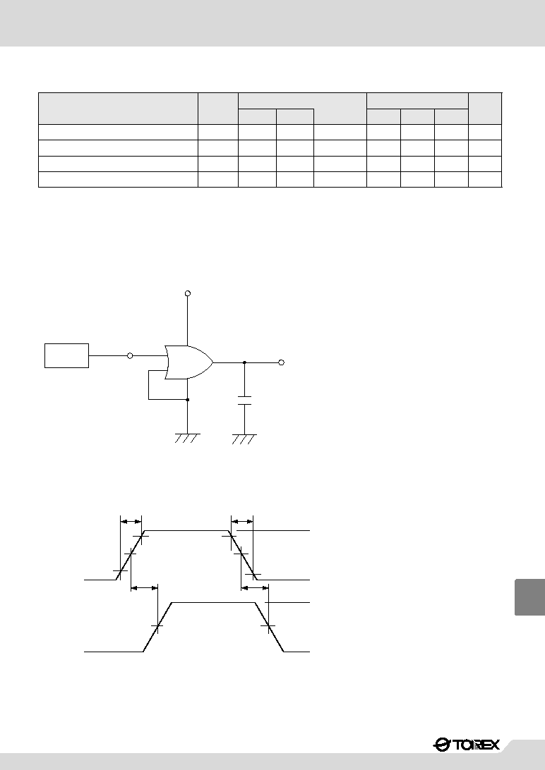
Typical Application Circuit
Waveforms
INPUT
OUTPUT
Pulse
Generator
V
CC
C
L
Z
OUT
=50
tr
tf
90%
10%
50%
INPUT
90%
50%
10%
50%
50%
OUTPUT
GND
V
CC
V
OH
V
OL
t
PLH
t
PHL
PRR=1MHz
duty cycle 50%
tr=tf=3ns
Noise Characteristics
( tr=tf=3ns )
PARAMETER
SYMBOL
CONDITIONS
Ta=25
UNITS
C
L
V
CC
(V)
Not functioning output maximum dynamic V
OL
V
OLP
50pF
5.0
-
0.3
0.8
V
V
Not functioning output minimum dynamic V
OL
V
OLV
50pF
5.0
-0.8
-0.3
-
Minimum dynamic V
IH
V
IHD
50pF
5.0
-
-
3.5
V
Maximum dynamic V
IL
V
ILD
50pF
5.0
-
-
1.5
V
MIN
TYP
MAX
XC74WL32AASR
909
13
13S_07XC74WL32AASR 02.09.12 15:56 909