
PWM Controlled Step-Up DC/DC Controllers
Series
387
4
The XC9101 series are step-up multiple current and voltage feedback
DC/DC controller ICs. Current sense, clock frequencies and amp
feedback gain can all be externally regulated.
A stable power supply is possible with output currents of up to 1.5A.
With output voltage fixed internally, V
OUT
is selectable in 0.1V steps
within a 2.5V - 16.0V range (± 2.5%).
For output voltages outside this range, we recommend the FB version
which has a 0.9V internal reference voltage. Using this version, the
required output voltage can be set-up using 2 external resistors.
Switching frequencies can also be set-up externally within a range of
100~600 kHz and therefore frequencies suited to your particular
application can be selected.
With the current sense function, peak currents (which flow through
the driver transistor and the coil) can be controlled. Soft-start time can
be adjusted using external resistor and capacitor.
During shutdown (CE pin =L), consumption current can be reduced to
as little as 0.5
µA (TYP.) or less.
General Description
GStable Operations via Current & Voltage Multiple Feedback
GUnlimited Options for Peripheral Selection
GCurrent Protection Circuit
GCeramic Capacitor Compatible
GMobile, Cordless phones
GPalm top computers, PDAs
GPortable games
GCameras, Digital cameras
GLaptops
Features
Applications
NInput Voltage Range : 2.5V ~ 20V
NOutput Voltage Range
: 2.5V ~ 16V
(Fixed Voltage Type)
: 30V + (Adjustable Type)
NOscillation Frequency Range
: 100kHz ~ 600kHz
NOutput Current
: up to 1.5A
NCeramic Capacitor Compatible
NMSOP-8A Package
V
IN
=2.5V
4.2V
3.3V
40
60
80
100
1
10
100
1000
Output Current : I
OUT
(mA)
Efficiency : EFFI (%)
CLK 5
1 EXT
2 Isen
3 V
IN
4 CE/SS
V
OUT
7
GAIN 6
Vss 8
U3FWJ44N
50m
22H
220F
+10F
150k
0.1F
1F
22K
XP161A1355PR
180pF
470pF
94F
Typical Application Circuit
Typical Performance
Characteristic
V
OUT
:5.0V FOSC:180kHz
04S_01XC9101/9102 02.09.12 14:37 387

XC9101
Series
388
4
Pin Configuration
Product Classification
GOrdering Information
1
2
3
4
6
5
7
8
EXT
Isen
V
IN
CESS
CCGAIN
CLK
V
OUT
FB
V
SS
MSOP-8A
(TOP VIEW)
DISIGNATOR SYMBOL
Soft-start
C
V
OUT
(Fixed Voltage Type)
D
Number
FB
A
Adjustable Frequency
K
R
Embossed tape. Standard Feed
Embossed tape. Reverse Feed
L
Output Voltage : For voltages above 10V, see below :
10=A, 11=B, 12=C, 13=D, 14=E, 15=F, 16=H
e.g. V
OUT
=2.3Vw=2, e=3 V
OUT
=13.5Vw=D, e=5
FB productsw=0, e=9 fixed
Soft-start externally set-up
Soft-start externally set-up
V
OUT
/FB
MSOP-8A
The standard output voltages of the XC9101C series are 2.5V, 3.3V, and 5.0V.
Voltages other than those listed are semi-custom.
qwerty
q
y
t
r
we
Pin Assignment
PIN NUMBER
PIN NAME
FUNCTION
1
EXT
Driver
2
Isen
Current Sense
3
V
IN
Power Input
4
CESS
CE/Soft Start
5
CLK
Clock Input
6
CCGAIN
Phase Compensation
7
V
OUT
FB
Voltage Sense
8
V
SS
Ground
Packaging Information
GMSOP-8A
3.00±0.10
4.90±0.10
3.00±0.10
0.53±0.13
0 6
0.000.20
0.30
+0.08
-0.02
1.02
0.86
+0.11 -0.10
+0.20 -0.21
0.15
+0.08
-0.02
(0.65)
04S_01XC9101/9102 02.09.12 14:38 388

XC9101
Series
389
4
Marking
q Represents the product series
w Represents product type, DC/DC converter
e Represents integral number of output voltage, or FB type
r Represents decimal number of output voltage
t Represents oscillation frequency's control type
DESIGNATOR
4
PRODUCT NAME
XC9101***AK*
DESIGNATOR
C
PRODUCT NAME
XC9101C**AK*
D
TYPE
V
OUT
, CE PIN
FB, CE PIN
XC9101D09AK*
PRODUCT NAME
2
VOLTAGEV
2. X
XC9101C2*AK*
3
3. X
XC9101C3*AK*
4
4. X
XC9101C4*AK*
5
5. X
XC9101C5*AK*
6
6. X
XC9101C6*AK*
7
7. X
XC9101C7*AK*
8
8. X
XC9101C8*AK*
9
9. X
XC9101C9*AK*
0
FB products
XC9101D09AK*
A
PRODUCT NAME
XC9101CA*AK*
B
10. X
11. X
XC9101CB*AK*
C
12. X
XC9101CC*AK*
D
13. X
XC9101CD*AK*
E
14. X
XC9101CE*AK*
F
15. X
XC9101CF*AK*
H
16. X
XC9101CH*AK*
DESIGNATOR
0
PRODUCT NAME
XC9101C*0AK*
3
VOLTAGEV
X. 0
X. 3
XC9101C*3AK*
9
FB products
XC9101D09AK*
DESIGNATOR
A
PRODUCT NAME
XC9101***AK*
TYPE
Adjustable Frequency
DESIGNATOR
DESIGNATOR VOLTAGEV
MSOP-8A
04S_01XC9101/9102 02.09.12 14:38 389
XC9101
Series
390
4
Absolute Maximum Ratings
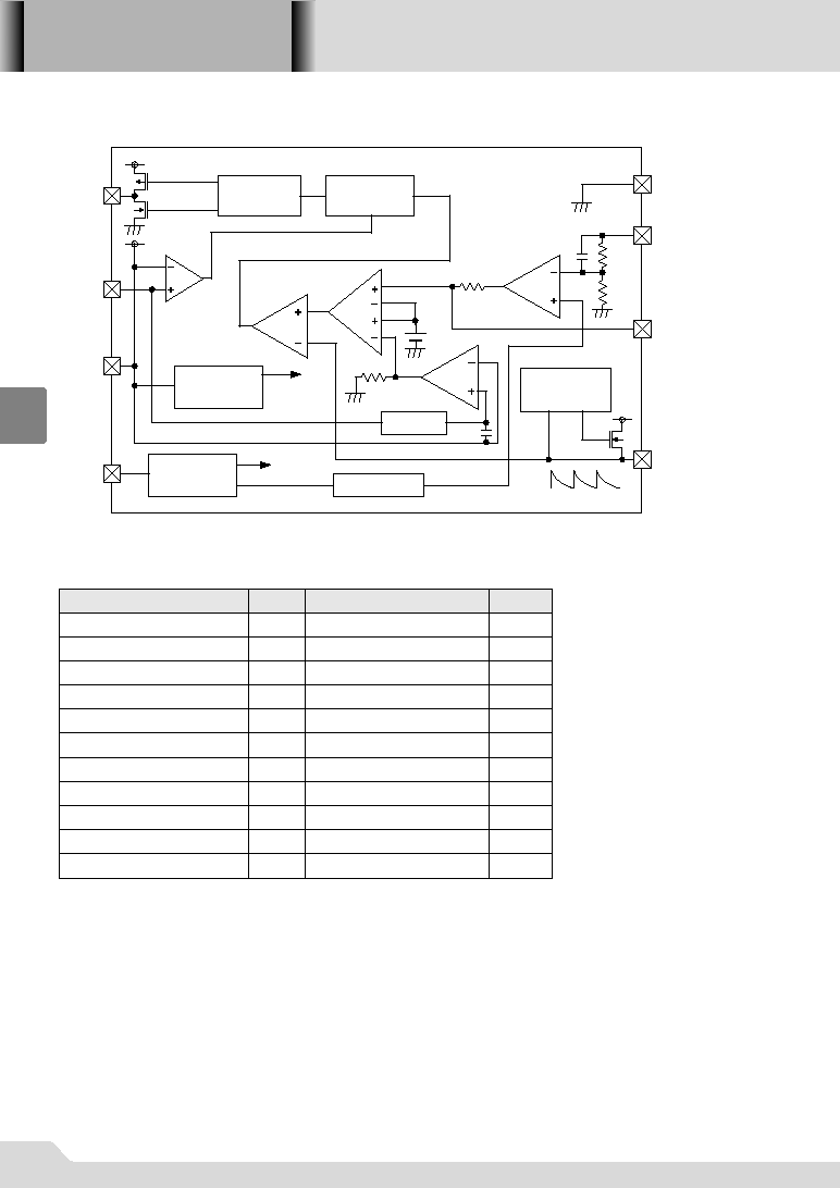
Block Diagram
EXT
ISEN
V
IN
CE/SS
V
SS
V
OUT
CC/GAIN
CLK
Ramp Wave,
Internal CLK
generator
Chip Enable,
Soft Start up,
U.V.L.O.
Verr
PWM
Ierr
Internal
Voltage
Regulator
EXT timming
controll
logic
Current
Limit
Protection
Limitter comp.
Vref generator
CE,UVLO
to internal
circuit
0.9V
Sampling
R1
R2
MIX
2.0V
to internal
circuit
PARAMETER
EXT Pin Voltage
Isen Pin Voltage
V
IN
Pin Voltage
CE/SS Pin Voltage
CLK Pin Voltage
CC/GAIN Pin Voltage
V
OUT
/FB Pin Voltage
EXT Pin Current
Continuous Total Power Dissipation
Operating Ambient Temperature
Storage Temperature
SYMBOL
RATINGS
UNITS
-0.322
V
EXT
VIsen
V
IN
V
CE
V
CLK
V
OUT
/FB
I
EXT
Tstg
-0.3V
DD
0.3
-0.322
-0.322
-0.3V
DD
0.3
-0.322
±100
-55125
mA
Pd
150
mW
Topr
-4085
Ta=25
V
CC
-0.3V
DD
0.3
04S_01XC9101/9102 02.09.12 14:38 390

XC9101
Series
391
4
Electrical Characteristics
XC9101C33AKR
V
IN
= 2.5V unless specified
*1 : EFFI = {[(Output Voltage)
◊ (Output Current)] ˜ [(Input Voltage) ◊ (Input Current)]} ◊ 100
*2 : The capacity range of the capacitor used to set the external CLK frequency is 150 ~ 220pF
Ta=25
SYMBOL
CONDITIONS
MIN.
TYP.
MAX.
UNITS
V
IN
max
V
OUT
V
IN
min
I
DD
1
I
STB
F
OSC
F
OSC
V
IN
F
OSC
F
OSC
ToprF
OSC
MAXDTY
MINDTY
I
LIM
I
ISEN
I
CEH
I
CEL
V
CEH
V
IN
=2.5V
V
OUT
=CE=Set Output Voltage◊0.95V
V
IN
=2.5V, CE=V
IN
V
OUT
=Set Output Voltage◊1.05V
V
IN
=2.5V, CE=V
OUT
=V
SS
RT=10.0k, CT=220pF
V
IN
=2.5V20V
Topr=-40+85
V
IN
=2.5V
I
OUT
=300mA
V
OUT
=Set Voltage◊0.95V
V
OUT
=Set Voltage◊1.05V
V
IN
pin voltage-I
SEN
pin voltage
V
IN
=2.5V, I
SEN
=2.5V
CE=V
IN
=2.5V, V
OUT
=0V
CE=0V, V
IN
=2.5V, V
OUT
=0V
Existence of CLK Oscillation,
V
OUT
=0V, CE : Voltage applied
Disappearance of CLK Oscillation,
V
OUT
=0V, CE : Voltage applied
EXT=V
IN
-0.4V, CE=V
IN
=2.5V
V
OUT
=Set voltage◊0.95V
EXT=0.4V, CE=V
IN
=2.5V
V
OUT
=Set voltage◊1.05
Connect C
SS
and R
SS
, CE : 0V2.5V
3.218
20
-
280
79
90
4.5
-0.1
-0.1
0.6
5
3.300
-
-
150
90
85
0.5
330
±5
±5
150
7
0
0
3.382
-
2.5
255
176
2.0
380
0
220
13
0.1
0.1
V
V
V
A
A
A
kHz
%
%
%
%
mV
A
A
A
V
V
CEL
0.2
V
R
EXTH
31
58
89
R
EXTL
27
45
20
EFFI
88
%
T
SS
10
ms
R
CCGAIN
400
k
CIRCUITS
q
q
q
w
w
w
e
e
e
r
r
y
y
t
t
t
t
r
r
q
q
u
I
DD
2
PARAMETER
Maximum Operating Voltage
Minimum Operating Voltage
Supply Current 1
Stand-by Current
Frequency Temperature
Fluctuation
Maximum Duty Cycle
Output Voltage
CLK Oscillation Frequency
Frequency Input Stability
Current Limiter Voltage
I
SEN
Current
CE "High" Current
CE "Low" Current
CE "High" Voltage
CE "Low" Voltage
EXT "High" ON
Resistance
EXT "Low" ON
Resistance
Efficiency *1
Soft-Start Time
CC/GAIN Pin
Output Impedance
Supply Current 2
Minimum Duty Cycle
04S_01XC9101/9102 02.09.12 14:38 391