 | –≠–ª–µ–∫—Ç—Ä–æ–Ω–Ω—ã–π –∫–æ–º–ø–æ–Ω–µ–Ω—Ç: XC9104 | –°–∫–∞—á–∞—Ç—å:  PDF PDF  ZIP ZIP |

June 25, 2003 Ver. 6
!
Ceramic Capacitors Compatible
"
APPLICATIONS
!
Input Voltage Range: 0.9V~10.0V
#
PDAs
!
Output Voltage Externally Set-up
#
Cellular Phones
!
Oscillation Frequency: 300kHz, 180kHz (±15%)
#
Palmtop Computers
!
PWM Control (XC9103)
#
Portable Audio Systems
PWM/PFM Automatic Switching Control (XC9104)
#
Various Multi-function Power Supplies
PWM/PFM Manual Switching Control (XC9105)
!
SOT-25 / USP-6B Package
"
GENERAL DESCRIPTION
"
FEATURES
Input Voltage Range:
0.9V ~ 10V
Power Supply Voltage Range:
1.8V ~ 10V
Output Voltage Range:
1.5V ~ 30V
Oscillation Frequency:
300, 180kHz ±15%
100, 500kHz available as semi-custom
Output Current:
more than 400mA
(VIN=1.8V, VOUT=3.3V)
Controls:
PWM (XC9103)
PWM/PFM auto-switching (XC9104)
PWM/PFM manual switching (XC9105)
High Efficiency:
85% (TYP.)
Stand-by Current:
ISTB=1
.0µ
A (MAX.)
Load Capacitors:
Low ESR capacitors compatible
Current Limiter Function:
Operates when ripple voltage
=250mV (180kHz version)
Packages :
SOT-25 / USP-6B
"
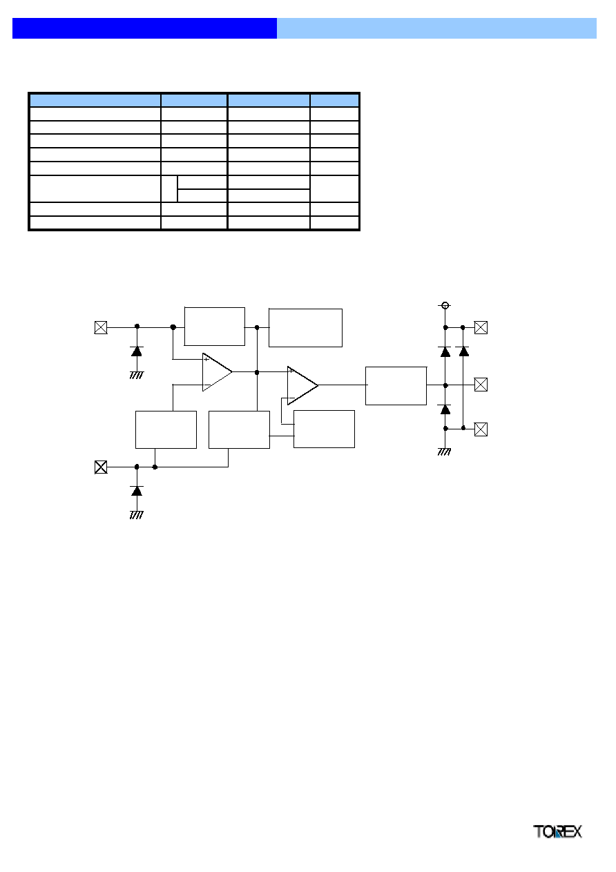
TYPICAL APPLICATION CIRCUIT
"
TYPICAL PERFORMANCE CHARACTERISTICS
(100kHz and 500kHz types are
available only without current limiter)
XC9103/04/05 Series
Ceramic Cap. Compatible
Step-Up DC/DC Converters
Also available without current limiter
Set up freely with a standard
voltage supply of 0.9V (±2.0%) &
external components
The XC9103/9104/9105 series are PWM, PWM/PFM auto switching
/manual switching controlled multi-functional step-up DC/DC converter
controllers.
Output will be stable no matter which load capacitors are used but should a
low ESR capacitor be used, RSENSE of about 0.1
will be required and
phase compensation will be achieved. This makes the use of ceramic
capacitors much easier and allows for lower output ripple and reduced PCB
area requirements. Tantalum and electrolytic capacitors can also be used,
in which case, RSENSE becomes unnecessary.
With 0.9V of standard voltage supply internal, and using externally
connected components, output voltage can be set up freely within a range
of 1.5V to 30V. With 300kHz or 180kHz frequencies, the size of the
external components can be reduced. Oscillation frequencies of 100kHz
and 500kHz are also available as custom-designed products.
The XC9103 series are PWM controlled. Control switches from PWM
to PFM during light loads with the XC9104 and the series is highly
efficient from light loads to large output currents. By using external signals,
control of the XC9105 can be alternated between PWM and
PWM/PFM automatic switching and so, control suited to the
application can be selected.
A current limiter circuit is built in to the IC (except with the 100kHz and
500kHz version) and monitors the ripple voltage on the FB pin. Operation
is shut down when the ripple voltage is more than 250mV(180kHz version).
The operations of the IC can be returned to normal with a toggle of the CE
pin or by turning the power supply back on.
0
20
40
60
80
100
0.1
1
10
100
1000
Output Current IOUT (mA)
Effi
ci
e
n
cy EF
F
I
(
%
)
VIN=0.9V
1.8V
1.2V
1.5V
2.7V
VOUT=3.3V
IOUT=400mA
Nch Power
MOS FET
XP161A1355
RSENSE:100m
for Ceramic CL
L: 10
µ
H
VIN
0.9V~
SD: MA737
RFB1:
120k
CFB: 47pF
RFB2:
45k
CE
(CE/PWM)
1
5
4
3
2
Ceramic CL
10
µ
F for 200mA
10
µ
Fx2 for
400mA
XC9105D093MR
VOUT=3.3V, CL=20uF
When PWM/PFM Automatic Switching
Tr: XP161A1355PR
Semiconductor Ltd.
1

"
PIN CONIGURATION
"
PIN ASSIGNMENT
"
ORDERING INFORMATION
XC9104 Series: PWM/PFM automatic switching control
XC9103 Series: PWM Control
(Same as XC9103 Series)
With Current Limiter
XC9105 Series: PWM/PFM manual switching control
(Same as XC9103 Series)
Oscillation Frequency:
300kHz
100kHz
180kHz
500kHz (D type only)
Package:
SOT-25 (1 reel = 3000 pcs.)
USP-6B (1 reel = 3000 pcs.)
Embossed Tape:
Standard Feed
Reverse Feed
"
PACKAGING INFORMATION
$
SOT-25 (SOT-23-5)
$
USP-6B
CE
Ground
Serves as both PWM/PFM switching pin
and CE pin for XC9105
(/PWM)
GND
FB
VDD
FB Voltage
5
6
R
PIN
NAME
XC9104
123456
Output Resistor Connection
Supply Voltage
Chip Enable (Operates in "H" level)
CE
FUNCTION
NC
No Connection
External Transistor Connection
EXT
XC9105
123456
3
1
PIN NUMBER
1
2
6
2
SOT-25 USP-6B
XC9103/04/05 Series
Ceramic Cap. Compatible
Step-Up DC/DC Converters
XC9103
123456
-
5
3
4
4
5
4
B
Without Current Limiter
(D type : 100kHz, 500kHz Only)
1
2
3
D
09
3
1
2
5
M
D
L
SOT-25
(TOP VIEW)
1
2
3
4
5
[SOT-23-5]
6
5
4
1
2
3
USP-6B
(TOP VIEW)
6
5
4
1
2
3
A
'
A
AAA
A
A
A
1
.
4
5
6
3
2
1
0
1
1
1
1
1
2.0 + 0.15
(0.45) 0.5+0.1
(0.05)
(0.45) (0.45)
45
O
45
O
1.
8+0.
15
(0
.2
7
)
(
0
.
27)
(0
.
2
7
)
(
0
.
4
5
)
45
O
45
O
(0
.1
2
5
)
(0
.6
5
)
0.
005
+0.
0
02
(0
.
0
5
)
-0
.
0
0
5
+0
.
0
1
-0
.
0
5
+0
.
1
5
0.7+0.03
5-
0.
2+0.
05
0.
5+0.
1
1.
6
+
0.
15
0.
5+0.
1
0.
1+0.
03
0.
2+0.
05
1.0+0.1
0.25+0.1
0.25+0.1
Semiconductor Ltd.
2
"
ABSOLUTE MAXIMUM RATINGS
Ta = 25
O
C
"
BLOCK DIAGRAM
-0.3 ~ VDD + 0.3
O
C
-40 ~ +125
Storage Temperature
mW
O
C
V
-0.3 ~ 12
-0.3 ~ 12
V
±100
150
100
-40 ~ +85
IEXT/
mA
VEXT
V
-0.3 ~ 12
RATINGS
UNITS
V
Operating Ambient Temperature
PARAMETER
VDD pin Voltage
FB pin Voltage
CE pin Voltage
EXT pin Voltage
EXT pin Current
Power Dissipation
VDD
FB
VCE
Topr
Tstg
XC9103/04/05 Series
Ceramic Cap. Compatible
Step-Up DC/DC Converters
Pd
SOT-25
USP-6B
SYMBOL
Note:
FB, CE : CMOS INPUT
EXT : CMOS OUTPUT
Ramp Wave
Generator,
OSC
Current
Ripple Detect
and FB
PWM/PFM
Controller
Phase
Compensation
Vref with
Soft Start,
CE
Buffer,
Driver
Error Amp.
PWM
Comparator
FB
VDD
EXT
GND
CE(/PWM)
Semiconductor Ltd.
3
"
ELECTRICAL CHARACTERISTICS
XC9103B092MR, XC9104B092MR, XC9105B092MR
XC9103D092MR, XC9104D092MR, XC9105D092MR
(FOSC=180 (kHz)
Ta=25
O
C
*1
*1
*3
*2
*2
Test Conditions: Unless otherwise stated, CL: ceramic capacitor, recommended MOS FET should be connected.
VOUT=3.30 (V), VIN=2.00 (V), IOUT=170 (mA)
"
NOTES
*1
*2
*3
5
5
-0.1
Same as IDD2, FB=VDD
4
4
5
5
5
5
1
1
1
6
1
1
4
5
4
4
-
3
4
3
µ
A
µ
A
µ
A
V
V
V
V
%
mV
%
mS
Same as IDD1, VEXT=0.4V
Same as IDD2, CE=VDD
Same as IDD2, CE=0V
V
V
V
V
V
µ
A
µ
A
Operation Start Voltage
VST1
-
Recommended Circuit using XP161A1355
Same as IDD1
Same as IDD1
Same as IDD1, VEXT=VOUT-0.4V
Output Voltage Range
VOUTSET
1.5
30.0
-
0.9
-
-
0.7
0.8
VHLD
Operation Holding Voltage
Recommended Circuit using 2SD1628,
IOUT=1.0mA
Same as VST2, VDD=3.300V
Same as IDD1, FB=1.2V
Same as IDD1, CE=0V
0.882
CIRCUIT
1
2
4
VLMT
Overcurrent SENSE Voltage
170
250
330
UNITS
MAX.
CONDITIONS
PARAMETER
Output Voltage
FB Control Voltage
Power Supply Voltage Range
MIN.
TYP.
VIN=VOUTSET
◊
0.6, VDD=3.3V
IOUT=10mA, Using 2SD1628
Oscillation Start Voltage
VST2
-
-
Supply Current 1
17
-
Stand-by Current
V
3.300
3.366
0.900
0.918
V
XC9103/04/05 Series
3.234
Ceramic Cap. Compatible
Step-Up DC/DC Converters
Supply Current 2
45
64
-
4
-
1.0
153
180
207
-
kHz
24
µ
A
81
87
20
28
36
75
%
85
Recommended Circuit using 2SD1628,
IOUT=1.0mA
No external connections
CE connected to VDD, Voltage applied, FB=0V
Same as IDD1
Same as IDD1
No Load (XC9104B/D, 9105B/D)
Maximum Duty Ratio
PWM Duty Ratio
FOSC
MAXDTY
PFMDTY
Oscillation Frequency
VFB
VDD
ISTB
IDD1
IDD2
20.0
5.0
10.0
Step input to FB ( Pulse width:2.0
µ
S or more)
EXT = Low level voltage
(XC9103B, 9104B, 9105B)
Soft-start Time
TSS
Efficiency
EFFI
CE "Low" Voltage
VCEL
CE "High" Voltage
VCEH
-
0.65
-
-
0.20
-
-
PWM "Low" Voltage
VPWML
PWM "High" Voltage
VPWMH
36
VDD - 1.0
IOUT=1.0mA (XC9105B/D)
IOUT=1.0mA (XC9105B/D)
-
VDD - 0.2
24
EXT "Low" ON Resistance
REXTL
EXT "High" ON Resistance
REXTH
-
16
-
24
-
-
-
0.1
-
-0.1
CE "Low" Current
ICEL
CE "High" Current
ICEH
FB "High" Current
IFBH
0.1
-
-
-
-
With the XC9105 series, the CE pin also serves as a PWM/PFM switching pin. In operation, PWM control is selected when the voltage at the CE pin is
more than VDD -0.2V. On the other hand, PWM/PFM automatic switching control at a duty = 25% is selected when the voltage at the CE pin is less than
VDD -1.0V and more than VCEH.
The overcurrent limit circuit of this IC is designed to monitor the ripple voltage so please select your external components carefully to prevent VLMT
being reached under low temperature conditions as well as normal operating conditions. Following current limiter circuit operations, which in turn causes
the IC's operations to stop, the operations of the IC can be returned to normal with a toggle of the CE pin or by turning the power supply back on.
FB "Low" Current
IFBL
Although the IC starts step-up operations from a VDD of 0.8V, the output voltage and oscillation frequency are stabilized at
VDD
1.8V. Therefore, a VDD of more than 1.8V is recommended when VDD is supplied from VIN or other power sources.
Same as IDD2, FB=0V
µ
A
-
1.8
-
10
SYMBOL
VOUT
Semiconductor Ltd.
4
"
ELECTRICAL CHARACTERISTICS (Continued)
XC9103B093MR, XC9104B093MR, XC9105B093MR
XC9103D093MR, XC9104D093MR, XC9105D093MR
(FOSC=300 (kHz)
Ta=25
O
C
*1
*1
*3
*2
*2
Test Conditions: Unless otherwise stated, CL: ceramic, recommended MOS FET should be connected.
VOUT=3.30 (V), VIN=2.00 (V), IOUT=170 (mA)
"
NOTES
*1
*2
*3
-
-0.1
µ
A
5
FB "Low" Current
IFBL
Same as IDD2, FB=0V
-
-
0.1
µ
A
5
FB "High" Current
IFBH
Same as IDD2, FB=VDD
-
0.1
µ
A
5
Same as IDD2, CE=0V
-
-
-0.1
µ
A
5
Same as IDD2, CE=VDD
36
4
Same as IDD1, VEXT=0.4V
-
16
24
4
24
-
V
1
IOUT=1.0mA (XC9105B/D)
-
-
VDD - 1.0
V
1
IOUT=1.0mA (XC9105B/D)
V
5
Same as IDD1
-
-
0.20
V
5
-
-
%
1
5.0
10.0
20.0
mS
1
Recommended Circuit using XP161A1355
380
mV
6
EXT = Low level voltage
(XC9103B, 9104B, 9105B)
4
PWM Duty Ratio
PFMDTY No Load (XC9104B/D, 9105B/D)
24
32
40
%
1
Same as IDD1
1.0
µ
A
5
Same as IDD1
255
300
345
kHz
4
88
µ
A
4
Same as IDD1, FB=1.2V
16
22
µ
A
4
Same as VST2, VDD=3.300V
0.7
V
3
IOUT=1.0mA
0.9
V
3
IOUT=1.0mA
-
V
4
1.8
-
10
V
-
0.882
0.900
0.918
V
1
Output Voltage Range
VOUTSET
VIN=VOUTSET
◊
0.6, VDD=3.3V
1.5
30.0
V
2
IOUT=10mA, Using 2SD1628
3.234
3.300
3.366
CONDITIONS
MIN.
TYP.
MAX.
UNITS
CIRCUIT
Although the IC starts step-up operations from a VDD of 0.8V, the output voltage and oscillation frequency are stabilized at
VDD
1.8V. Therefore, a VDD of more than 1.8V is recommended when VDD is supplied from VIN or other power sources.
With the XC9105 series, the CE pin also serves as a PWM/PFM switching pin. In operation, PWM control is selected when the voltage at the CE pin is
more than VDD -0.2V. On the other hand, PWM/PFM automatic switching control at a duty = 25% is selected when the voltage at the CE pin is less than
VDD -1.0V and more than VCEH.
The overcurrent limit circuit of this IC is designed to monitor the ripple voltage so please select your external components carefully to prevent VLMT
being reached under low temperature conditions as well as normal operating conditions. Following current limiter circuit operations, which in turn causes
the IC's operations to stop, the operations of the IC can be returned to normal with a toggle of the CE pin or by turning the power supply back on.
CE "Low" Current
ICEL
CE "High" Current
ICEH
-
-
EXT "Low" ON Resistance
REXTL
EXT "High" ON Resistance
REXTH
Same as IDD1, VEXT=VOUT-0.4V
-
PWM "Low" Voltage
VPWML
PWM "High" Voltage
VPWMH
VDD - 0.2
-
CE "Low" Voltage
VCEL
CE "High" Voltage
VCEH
Same as IDD1
0.65
Soft-start Time
TSS
Efficiency
EFFI
-
85
Overcurrent SENSE Voltage
VLMT
Step input to FB ( Pulse width:2.0
µ
S or more)
220
300
75
81
87
%
Maximum Duty Ratio
MAXDTY
Oscillation Frequency
FOSC
Stand-by Current
ISTB
Same as IDD1, CE=0V
Supply Current 2
IDD2
Supply Current 1
IDD1
62
Operation Holding Voltage
VHLD
Recommended Circuit using 2SD1628,
-
-
4
Oscillation Start Voltage
VST2
No external connections
CE connected to VDD, Voltage applied, FB=0V
-
-
0.8
V
Operation Start Voltage
VST1
Recommended Circuit using 2SD1628,
-
SYMBOL
Power Supply Voltage Range
VDD
FB Control Voltage
VFB
Output Voltage
VOUT
PARAMETER
XC9103/04/05 Series
Ceramic Cap. Compatible
Step-Up DC/DC Converters
-
Semiconductor Ltd.
5

"
TYPICAL APPLICATION CIRCUIT
"
HOW TO USE
Note:
* Please select your external components carefully (refer to the page 8).
By using external signals, the control of the XC9105 series can be switched between PWM control
and PWM/PFM automatic switching control. By inputting a voltage of more than VDD -0.2V to the
CE/PWM pin, PWM control can be selected. On the other hand, PWM/PFM automatic switching
control can be selected by inputting a voltage of less than VDD -1.0V.
Insert Rb and CB when using a
bipolar NPN Transistor.
When obtaining VDD from a source other than
VOUT, please insert a capacitor CIN between
the VDD pin and the GND pin in order to provide
stabler operations.
Please wire CL & CIN between the VOUT/VDD
pin and the GND pin. Strengthen the wiring
sufficiently.
With the XC9105, by connecting resistors of the same value (RM1, RM2) as shown in the diagram
to the left, it is possible to obtain chip disable with SCE ON and, SPWM ON or OFF, PWM/PFM
auto switching at Duty=25% with SCE OFF & SPWM ON, & PFM control with both switches OFF.
When operating at VDD -1.8V and below (stepping-up from VIN=0.9V), it is necessary to pull-up to
VDD in order to allow the CE/PWM pin reach the VCEH voltage level. Please make sure that the
IC is in PWM control (SPWM=OFF) when operations start. If SPWM is ON, there are times when
chip enable might not operate.
SCE
ON
PWM
OFF
OFF
OFF
Chip Disable
CONDITIONS
SPWM
ON or OFF
ON
Duty=25%, PWM/PFM automatic switching
XC9103/04/05 Series
Ceramic Cap. Compatible
Step-Up DC/DC Converters
Semiconductor Ltd.
VOUT
Nch Power
MOS FET
RSENSE
L
VIN
SD
RFB1
RFB2
CFB
CE
(CE/PWM)
1
5
4
3
2
CL
Rb
Cb
VDD
RM1
RM2
SCE
SPWM
CE/PWM
6

"
NOTE ON HOW TO USE B TYPE
Please set time constant equal to 10ms by the following equation.
Time constant :
(s) = R (
) x C (F)
[ Example of Equation ]
R = 100k
, C = 0.1
µ
F
(s)
= R (
) x C (F)
= 100k
x 0.1
µ
F = 10ms
"
OPERATIONAL DESCRIPTION
The XC9103/04/05 series are step-up DC/DC converter controller ICs with built-in high speed, low ON resistance drivers.
<Error Amp.>
<OSC Generator>
<Ramp Wave Generator>
The Ramp Wave Generator generates a saw-tooth waveform based on outputs from the OSC Generator.
<PWM Comparator>
<PWM/PFM Controller>
<Vref 1 with Soft Start>
<Enable Function>
XC9103/04/05 Series
Ceramic Cap. Compatible
Step-Up DC/DC Converters
Error Amplifier is designed to monitor the output voltage, comparing the feedback voltage (FB) with the reference voltage Vref. In response to feedback
of a voltage lower than the reference voltage Vref, the output voltage of the error amp. decreases.
This circuit generates the internal reference clock.
The PWM comparator compares outputs from the Error Amp. and saw-tooth waveform. When the voltage from the Error Amp's output is low, the
external switch will be set to ON.
This circuit generates PFM pulses.
The PWM/PFM automatic switching mode switches between PWM and PFM automatically depending on the load. The PWM/PFM automatic switching
mode is selected when the voltage of the CE pin is less than VDD - 1.0V, and the control switches between PWM and PFM automatically depending on
the load. PWM/PFM control turns into PFM control when threshold voltage becomes lower than voltage of error amps. PWM control mode is selected
when the voltage of the CE pin is more than VDD - 0.2V. Noise is easily reduced with PWM control since the switching frequency is fixed. The series is
suitable for noise sensitive portable audio equipment as PWM control can suppress noise during operation and PWM/PFM switching control can reduce
consumption current during light load in stand-by.
The reference voltage, Vref (FB pin voltage)=0.9V, is adjusted and fixed by laser trimming (for output voltage settings, please refer to the notes on page
8). To protect against inrush current, when the power is switched on, and also to protect against voltage overshoot, soft-start time is set internally to
10ms. It should be noted, however, that this circuit does not protect the load capacitor (CL) from inrush current. With the Vref voltage limited and
depending upon the input to the error amps, the operation maintains a balance between the two inputs of the error amps and controls the EXT pin's ON
time so that it doesn't increase more than is necessary.
This function controls the operation and shutdown of the IC. When the voltage of the CE pin is 0.2V or less, the mode will be disable, the channel's
operations will stop and the EXT1 pin will be kept at a low level (the external N-type MOSFET will be OFF). When the IC is in a state of disable, current
consumption will be no more than 1.0
µ
A.
When the CE pin's voltage is 0.65V or more, the mode will be enable and operations will recommence.
When applying voltage to VDD through CE pin with the series' B type product, the
limiter circuit may operate when a power supply is on, and the operation may not
start. In this case, as the right circuit indicates, please connect a resistor and a
capacitor with the CE pin. By the time constant, the CE pin will be chip enable after
VDD rise so that IC will be in the stable condition.
Semiconductor Ltd.
R
CE/PWM
EXT
GND
FB
VDD
C
7

"
FUNCTIONAL SETTINGS
< Output Voltage Setting>
VOUT = 0.9 x (RFB1 + RFB2) / RFB2
fzfb = 30kHz (L=10
µ
H)
[ Example of Equation ]
fzfb = 20kHz (L=22
µ
H)
RFB1 : 120k
RFB2 : 45k
fzfb = 10kHz (L=47
µ
H)
CFB :
47pF
(fzfb = 30kHz, L = 10
µ
H)
68pF
(fzfb = 20kHz, L = 22
µ
H)
130pF
(fzfb = 10kHz, L = 47
µ
H)
< The use of ceramic capacitor CL >
< External Components >
Tr:
*When a MOSFET is used :
*When a NPN Tr. Is used :
XP161A1355PR (TOREX Nch. Power MOSFET)
2SD1628 (Sanyo)
Rb
: 500
(adjust with Tr's HSE or load)
Cb
: 2200pF (ceramic type)
Cb
1 / (2
◊
Rb
◊
FOSC
◊
0.7)
SD:
MA2Q737 (Schottky type, MATSUSHITA)
L, CL:
When using ceramic type
L:
22
µ
H (SUMIDA CDRH5D28, FOSC = 100, 180kHz)
10
µ
H (SUMIDA CDRH5D18, FOSC = 300, 500kHz)
CL:
10V 10
µ
F (ceramic type, TAIYO YUDEN LMK325BJ106ML))
Use the formula below when step-up ratio and output current is large.
CL = (CL standard value) x (IOUT(mA) / 300mA x VOUT / VIN)
RSENSE:
100m
(FOSC = 180, 300, 500kHz)
50m
(FOSC = 100kHz)
CL:
Tantalum Type
L:
22
µ
H (SUMIDA CDRH5D28, FOSC = 300kHz)
47µ
H (SUMIDA CDRH5D28, FOSC = 100, 180kHz)
Except when IOUT(mA) / 100mA
◊
VOUT / VIN > 2
22
µ
H
10
µ
H (SUMIDA CDRH5D18, FOSC = 500kHz)
CL:
16V 47
µ
F (tantalum type NICHICHEMI 16MCE476MD2)
Use the formula below when step-up ratio and output current is large.
CL = (CL standard value)
◊
(IOUT(mA) / 300mA
◊
VOUT / VIN)
RSENSE:
Not required, but short out the wire.
CL:
AL Electrolytic Type
L:
22
µ
H (SUMIDA CDRH5D28, FOSC = 300kHz)
47µ
H (SUMIDA CDRH5D28, FOSC = 100, 180kHz)
Except when IOUT(mA) / 100mA
◊
VOUT / VIN > 2
22
µ
H
CL:
16V 100
µ
F (AL electrolytic type) + 10V 2.2
µ
F (ceramic type)
Strengthen appropriately when step-up ratio and output current is large.
RSENSE:
Not required, but short out the wire.
CFB:
Set up so that fzfb = 100kHz.
Output voltage can be set by adding external split resistors. Output voltage is determined by the following equation, based on the values of RFB1 and
RFB2. The sum of RFB1 and RFB2 should normally be 2 M
or less.
The value of CFB1, speed-up capacitor for phase compensation, should result in fzfb = 1/(2
◊
CFB
◊
RFB1) equal to 5 to 30kHz. Adjustments
are required depending on the application, value of inductance (L), and value of load capacity (CL).
The circuit of the XC9103/04/05 series is organized by a specialized circuit which reenacts negative feedback of both voltage and current. Also
by insertion of approximately 100m
of a low and inexpensive sense resistor as current sense, a high degree of stability is possible even using
a ceramic capacitor, a condition which used to be difficult to achieve. Compared to a tantalum condenser, because the series can be operated
in a very small capacity, it is suited to use of the ceramic capacitor which is cheap and small.
Note* : As the breakdown voltage of XP161A1355 is 8V, take
care with the power supply voltage. With output voltages over
6V, use the XP161A1265 with a breakdown voltage of 12V.
VST1: XP161A1355 PR =1.2V (max.)
XP161A1265PR = 1.5V (max.)
XC9103/04/05 Series
Ceramic Cap. Compatible
Step-Up DC/DC Converters
Semiconductor Ltd.
8

"
TEST CIRCUITS
CIRCUIT
1
CIRCUIT
4
CIRCUIT
2
CIRCUIT
5
CIRCUIT
6
CIRCUIT
3
XC9103/04/05 Series
Ceramic Cap. Compatible
Step-Up DC/DC Converters
V
IN
L
SD
Tr
EXT
C
IN
GND
VDD
FB
CE
C
L
CFB
RFB1
RFB2
A
R
L
V
OUT
V
A
OSC
RSENSE
C
E
V
DD
FB
EXT
CE
GND
A
A
A
L
SD
Tr
EXT
C
IN
GND
V
DD
FB
CE
C
L
C
FB
R
FB1
R
FB2
R
SENSE
C
B
OSC
V
IN
A
RB
A
R
L
V
A
L
SD
Tr
EXT
C
IN
GND
V
DD
FB
CE
C
L
C
FB
R
FB1
R
FB2
R
SENSE
C
B
OSC
V
IN
A
RB
R
L
V
A
EXT
GND
VDD
FB
CE
CFB
RFB1
RFB2
0.1uF
V
DD
FB
EXT
CE
GND
OSC
A
R
P
CDD
C
P
Semiconductor Ltd.
9
"
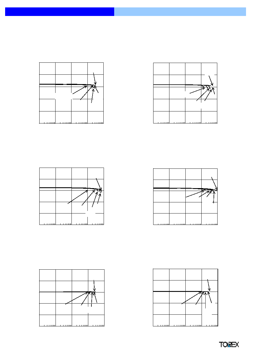
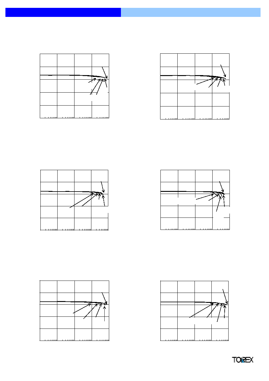
TYPICAL PERFORMANCE CHARACTERISTICS
(1) Output Voltage vs. Output Current
XC9103/04/05 Series
Ceramic Cap. Compatible
Step-Up DC/DC Converters
XC9103D092MR (PWM,180kHz,3.3V)
3.0
3.1
3.2
3.3
3.4
3.5
0.1
1
10
100
1000
Output Current I
OUT
(mA)
O
u
tput Voltage V
OUT
(V)
2.0V
VIN=0.9V
1.8V
1.2V
1.5V
L=22mH(CDRH5D28),CL=20mF(ceramic)
SD:MA2Q737 Tr:XP161A1355P
XC9104D092MR (PWM/PFM,180kHz,3.3V)
3.0
3.1
3.2
3.3
3.4
3.5
0.1
1
10
100
1000
Output Current IOUT(mA)
O
u
tput Voltage VO
U
T
(V)
2.0V
VIN=0.9V
1.8V
1.2V 1.5V
L=22
µ
H(CDRH5D28),CL=20
µ
F(ceramic)
SD:MA2Q737, Tr:XP161A1355P
XC9103D093MR (PWM,300kHz,3.3V)
3.0
3.1
3.2
3.3
3.4
3.5
0.1
1
10
100
1000
Output Current I
OUT
(mA)
O
u
tput Voltage V
OUT
(V)
2.0V
VIN=0.9V
1.8V
1.2V
L=10
µ
H(CDRH5D18),CL=20
µ
F(ceramic)
SD:MA2Q737, Tr:XP161A1355P
1.5V
XC9104D093MR (PWM/PFM,300kHz,3.3V)
3.0
3.1
3.2
3.3
3.4
3.5
0.1
1
10
100
1000
Output Current IOUT(mA)
O
u
tput Voltage V
OUT
(V)
VIN=0.9V
L=10
µ
H(CDRH5D18),CL=20
µ
F(ceramic)
SD:MA2Q737, Tr:XP161A1355P
2.7V
1.2V 1.5V
1.8V
XC9103D091MR (PWM,100kHz,3.3V)
3.0
3.1
3.2
3.3
3.4
3.5
0.1
1
10
100
1000
Output Current I
OUT
(mA)
O
u
tput Voltage V
OUT
(V)
2.0V
VIN=0.9V
1.2V 1.5V
L=22
µ
H(CDRH5D28),CL=20
µ
F(ceramic)
SD:MA2Q737, Tr:XP161A1355P
1.8V
XC9104D091MR (PWM/PFM,100kHz,3.3V)
3.0
3.1
3.2
3.3
3.4
3.5
0.1
1
10
100
1000
Output Current I
OUT
(mA)
O
u
tput Voltage V
OUT
(V)
2.0V
1.8V
1.2V
1.5V
L=22
µ
H(CDRH5D28),CL=20
µ
F(ceramic)
SD:MA2Q737, Tr:XP161A1355P
VIN=0.9V
Semiconductor Ltd.
10
(1) Output Voltage vs. Output Current (Contd.)
XC9103/04/05 Series
Ceramic Cap. Compatible
Step-Up DC/DC Converters
XC9103D095MR (PWM,500kHz,3.3V)
3.0
3.1
3.2
3.3
3.4
3.5
0.1
1
10
100
1000
Output Current I
OUT
(mA)
O
u
tput Voltage V
OUT
(V)
2.0V
VIN=0.9V
1.8V
1.2V 1.5V
L=10
µ
H(CDRH5D18), CL=20
µ
F(ceramic)
SD:MA2Q737, Tr:XP161A1355P
XC9104D095MR (PWM/PFM,500kHz,3.3V)
3.0
3.1
3.2
3.3
3.4
3.5
0.1
1
10
100
1000
Output Current I
OUT
(mA)
O
u
tput Voltage V
OUT
(V)
2.0V
VIN=0.9V
1.8V
1.2V
L=10
µ
H(CDRH5D18), CL=20
µ
F(ceramic)
SD:MA2Q737, Tr:XP161A1355P
1.5V
XC9103D092MR (PWM,180kHz,3.3V)
3.0
3.1
3.2
3.3
3.4
3.5
0.1
1
10
100
1000
Output Current I
OUT
(mA)
O
u
tput Voltage V
OUT
(V)
2.0V
VIN=0.9V
1.8V
1.2V
1.5V
L=22
µ
H(CDRH5D28),CL=47
µ
F(tantalum)
SD:MA2Q737, Tr:XP161A1355P
XC9104D092MR (PWM/PFM,180kHz,3.3V)
3.0
3.1
3.2
3.3
3.4
3.5
0.1
1
10
100
1000
Output Current I
OUT
(mA)
O
u
tput Voltage V
OUT
(V)
2.0V
VIN=0.9V
1.8V
1.2V
1.5V
L=22
µ
H(CDRH5D28), CL=47
µ
F(tantalum)
SD:MA2Q737, Tr:XP161A1355P
XC9103D093MR (PWM,300kHz,3.3V)
3.0
3.1
3.2
3.3
3.4
3.5
0.1
1
10
100
1000
Output Current I
OUT
(mA)
O
u
tput Voltage V
OUT
(V)
2.0V
VIN=0.9V
1.8V
1.2V
L=22
µ
H(CDRH5D28), CL=94
µ
F(tantalum)
SD:MA2Q737, Tr:XP161A1355P
XC9104D093MR (PWM/PFM,300kHz,3.3V)
3.0
3.1
3.2
3.3
3.4
3.5
0.1
1
10
100
1000
Output Current I
OUT
(mA)
O
u
tput Voltage V
OUT
(V)
VIN=0.9V
L=22
µ
H(CDRH5D28), CL=94
µ
F(tantalum)
SD:MA2Q737, Tr:XP161A1355P
2.0V
1.5V
1.2V
1.8V
Semiconductor Ltd.
11

(2) Efficiency vs. Output Current
XC9103/04/05 Series
Ceramic Cap. Compatible
Step-Up DC/DC Converters
XC9103D092MR (PWM,180kHz,3.3V)
0
20
40
60
80
100
0.1
1
10
100
1000
Output Current I
OUT
(mA)
E
fficiency E
FFI(
%
)
VIN=0.9V
1.2V
1.8V
1.5V
L=22
µ
H(CDRH5D28),CL=20
µ
F(ceramic)
SD:MA2Q737, Tr:XP161A1355P
2.0V
XC9104D092MR (PWM/PFM,180kHz,3.3V)
0
20
40
60
80
100
0.1
1
10
100
1000
Output Current I
OUT
(mA)
E
fficiency E
FFI(
%
)
VIN=0.9V
1.2V
1.8V
1.5V
L=22
µ
H(CDRH5D28), CL=20
µ
F(ceramic)
SD:MA2Q737, Tr:XP161A1355P
2.0V
XC9103D093MR (PWM,300kHz,3.3V)
0
20
40
60
80
100
0.1
1
10
100
1000
Output Current I
OUT
(mA)
E
fficiency E
FFI(
%
)
VIN=0.9V
1.2V
1.8V
1.5V
L=10
µ
H(CDRH5D18), CL=20
µ
F(ceramic)
SD:MA2Q737, Tr:XP161A1355P
2.0V
XC9104D093MR (PWM/PFM,300kHz,3.3V)
0
20
40
60
80
100
0.1
1
10
100
1000
Output Current I
OUT
(mA)
E
fficiency E
FFI(
%
)
VIN=0.9V
1.2V
1.8V
1.5V
L=10
µ
H(CDRH5D18),CL=20
µ
F(ceramic)
SD:MA2Q737, Tr:XP161A1355P
2.7V
XC9103D091MR (PWM,100kHz,3.3V)
0
20
40
60
80
100
0.1
1
10
100
1000
Output Current I
OUT
(mA)
E
fficiency E
FFI(
%
)
VIN=0.9V
1.2V
1.8V
1.5V
L=22
µ
H(CDRH5D28), CL=20
µ
F(ceramic)
SD:MA2Q737, Tr:XP161A1355P
2.0V
XC9104D091MR (PWM/PFM,100kHz,3.3V)
0
20
40
60
80
100
0.1
1
10
100
1000
Output Current I
OUT
(mA)
E
fficiency E
FFI(
%
)
VIN=0.9V
1.2V
1.8V
1.5V
L=22
µ
H(CDRH5D28), CL=20
µ
F(ceramic)
SD:MA2Q737, Tr:XP161A1355P
2.0V
Semiconductor Ltd.
12
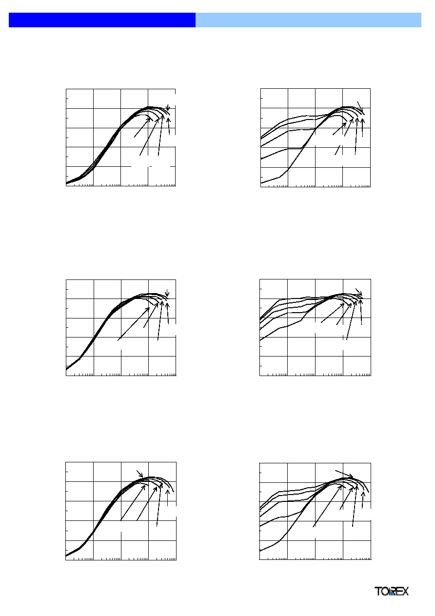
(2) Efficiency vs. Output Current (Contd.)
XC9103/04/05 Series
Ceramic Cap. Compatible
Step-Up DC/DC Converters
XC9103D095MR (PWM,500kHz,3.3V)
0
20
40
60
80
100
0.1
1
10
100
1000
Output Current I
OUT
(mA)
E
fficiency E
FFI(
%
)
1.2V
1.8V
1.5V
L=10
µ
H(CDRH5D18), CL=20
µ
F(ceramic)
SD:MA2Q737, Tr:XP161A1355P
2.0V
XC9104D095MR (PWM/PFM,500kHz,3.3V)
0
20
40
60
80
100
0.1
1
10
100
1000
Output Current I
OUT
(mA)
E
fficiency E
FFI(
%
)
VIN=0.9V
1.2V
1.8V
1.5V
L=10
µ
H(CDRH5D18), CL=20
µ
F(ceramic)
SD:MA2Q737, Tr:XP161A1355P
2.0V
XC9103D092MR (PWM,180kHz,3.3V)
0
20
40
60
80
100
0.1
1
10
100
1000
Output Current I
OUT
(mA)
E
fficiency E
FFI(
%
)
VIN=0.9V
1.2V
1.8V
1.5V
L=22
µ
H(CDRH5D28),CL=47
µ
F(tantalum)
SD:MA2Q737, Tr:XP161A1355P
2.0V
XC9104D092MR (PWM/PFM,180kHz,3.3V)
0
20
40
60
80
100
0.1
1
10
100
1000
Output Current I
OUT
(mA)
E
fficiency E
FFI(
%
)
VIN=0.9V 1.2V
1.8V
1.5V
L=22
µ
H(CDRH5D28), CL=47
µ
F(tantalum)
SD:MA2Q737, Tr:XP161A1355P
2.0V
XC9103D093MR (PWM,300kHz,3.3V)
0
20
40
60
80
100
0.1
1
10
100
1000
Output Current I
OUT
(mA)
E
fficiency E
FFI(
%
)
VIN=0.9V 1.2V
1.8V
1.5V
L=22
µ
H(CDRH5D28),CL=94
µ
F(tantalum)
SD:MA2Q737, Tr:XP161A1355P
2.0V
XC9104D093MR (PWM/PFM,300kHz,3.3V)
0
20
40
60
80
100
0.1
1
10
100
1000
Output Current I
OUT
(mA)
E
fficiency E
FFI(
%
)
VIN=0.9V
1.2V
1.8V
1.5V
L=22
µ
H(CDRH5D28), CL=94
µ
F(tantalum)
SD:MA2Q737, Tr:XP161A1355P
2.0V
Semiconductor Ltd.
13
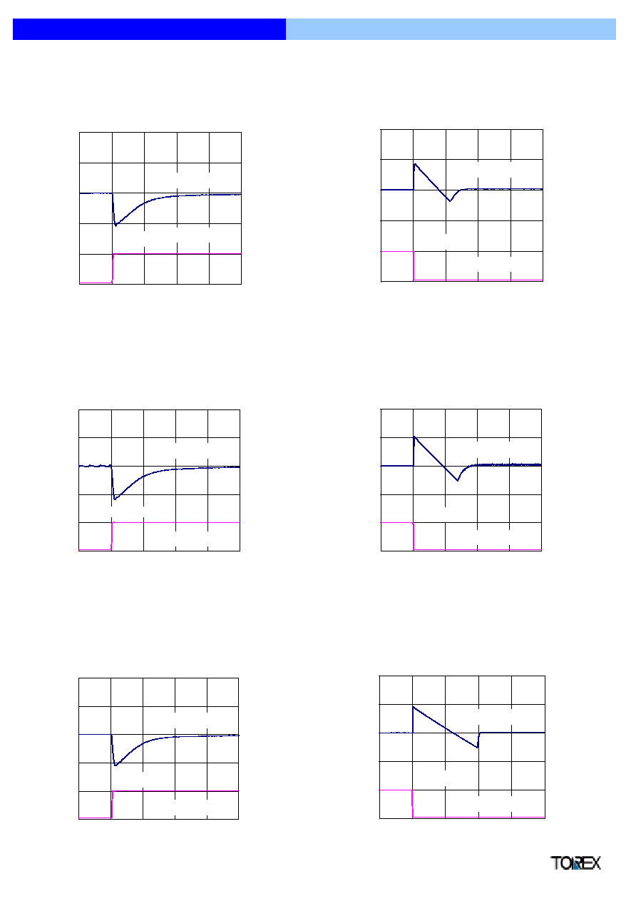
(3) Load Transient Response
XC9103/04/05 Series
Ceramic Cap. Compatible
Step-Up DC/DC Converters
XC9103D092MR(PWM,180kHz,3.3V)
3.0
3.1
3.2
3.3
3.4
3.5
Time (1.0msec/div)
O
u
tput Voltage V
OUT
(V)
0
100
200
300
400
500
O
u
tput C
u
rrent I
OUT
(m
A)
Output Voltage
100mA
Output Current
VIN=1.98V, CL=20
µ
F(ceramic), IOUT=100
µ
A
100mA
100
µ
A
XC9103D092MR(PWM,180kHz,3.3V)
3.0
3.1
3.2
3.3
3.4
3.5
Time (2.0msec/div)
O
u
tput Voltage V
OUT
(V)
0
100
200
300
400
500
O
u
tput C
u
rrent I
OUT
(m
A)
100mA
VIN=1.98V, CL=20
µ
F(ceramic), IOUT=100
µ
A
100mA
100
µ
A
Output Voltage
Output Current
XC9104D092MR(PWM/PFM,180kHz,3.3V)
3.0
3.1
3.2
3.3
3.4
3.5
Time (1.0msec/div)
O
u
tput Voltage V
OUT
(V)
0
100
200
300
400
500
O
u
tput C
u
rrent I
OUT
(m
A)
100mA
VIN=1.98V, CL=20
µ
F(ceramic), IOUT=100
µ
A
100mA
100
µ
A
Output Current
Output Voltage
XC9104D092MR(PWM/PFM,180kHz,3.3V)
3.0
3.1
3.2
3.3
3.4
3.5
Time (2.0msec/div)
O
u
tput Voltage V
OUT
(V)
0
100
200
300
400
500
O
u
tput C
u
rrent I
OUT
(m
A)
100mA
VIN=1.98V, CL=20
µ
F(ceramic), IOUT=100
µ
A
100mA
100
µ
A
Output Voltage
Output Current
XC9103D093MR(PWM,300kHz,3.3V)
3.0
3.1
3.2
3.3
3.4
3.5
Time (1.0msec/div)
O
u
tput Voltage V
OUT
(V)
0
100
200
300
400
500
O
u
tput C
u
rrent I
OUT
(m
A)
100mA
VIN=1.98V, CL=20
µ
F(ceramic), IOUT=100
µ
A
100mA
100
µ
A
Output Current
Output Voltage
XC9103D093MR(PWM,300kHz,3.3V)
3.0
3.1
3.2
3.3
3.4
3.5
Time (10.0msec/div)
O
u
tput Voltage V
OUT
(V)
0
100
200
300
400
500
O
u
tput C
u
rrent I
OUT
(m
A)
100mA
VIN=1.98V, CL=20
µ
F(ceramic), IOUT=100
µ
A
100mA
100
µ
A
Output Current
Output Voltage
Semiconductor Ltd.
14

(3) Load Transient Response (Contd.)
XC9103/04/05 Series
Ceramic Cap. Compatible
Step-Up DC/DC Converters
XC9104D093MR(PWM/PFM,300kHz,3.3V)
3.0
3.1
3.2
3.3
3.4
3.5
Time (1.0msec/div)
O
u
tput Voltage V
OUT
(V)
0
100
200
300
400
500
O
u
tput C
u
rrent I
OUT
(m
A)
100mA
VIN=1.98V, CL=20
µ
F(ceramic), IOUT=100
µ
A
100mA
100
µ
A
Output Current
Output Voltage
XC9104D093MR(PWM/PFM,300kHz,3.3V)
3.0
3.1
3.2
3.3
3.4
3.5
Time (10.0msec/div)
O
u
tput Voltage V
OUT
(V)
0
100
200
300
400
500
O
u
tput C
u
rrent I
OUT
(m
A)
100mA
VIN=1.98V, CL=20
µ
F(ceramic), IOUT=100
µ
A
100mA
100
µ
A
Output Current
Output Voltage
XC9103D092MR(PWM,180kHz,3.3V)
3.0
3.1
3.2
3.3
3.4
3.5
Time (1.0msec/div)
O
u
tput Voltage V
OUT
(V)
0
100
200
300
400
500
O
u
tput C
u
rrent I
OUT
(m
A)
100mA
VIN=1.98V, CL=47
µ
F(tantalum), IOUT=100
µ
A
100mA
100
µ
A
Output Current
Output Voltage
XC9103D092MR(PWM,180kHz,3.3V)
3.0
3.1
3.2
3.3
3.4
3.5
Time (4.0msec/div)
O
u
tput Voltage V
OUT
(V)
0
100
200
300
400
500
O
u
tput C
u
rrent I
OUT
(m
A)
100mA
VIN=1.98V, CL=47
µ
F(tantalum), IOUT=100
µ
A
100mA
100
µ
A
Output Current
Output Voltage
XC9104D092MR(PWM/PFM,180kHz,3.3V)
3.0
3.1
3.2
3.3
3.4
3.5
Time (1.0msec/div)
O
u
tput Voltage V
OUT
(V)
0
100
200
300
400
500
O
u
tput C
u
rrent I
OUT
(m
A)
100mA
VIN=1.98V, CL=47
µ
F(tantalum), IOUT=100
µ
A
100mA
100
µ
A
Output Current
Output Voltage
XC9104D092MR(PWM/PFM,180kHz,3.3V)
3.0
3.1
3.2
3.3
3.4
3.5
Time (4.0msec/div)
O
u
tput Voltage V
OUT
(V)
0
100
200
300
400
500
O
u
tput C
u
rrent I
OUT
(m
A)
100mA
100
µ
A
VIN=1.98V, CL=47
µ
F(tantalum), IOUT=100
µ
A
100mA
Output Voltage
Output Current
Semiconductor Ltd.
15

(4) Output Voltage vs. Power Supply Voltage
(5) Supply Current 1 vs. Power Supply Voltage
(6) Supply Current 2 vs. Power Supply Voltage
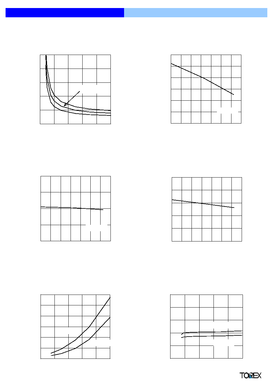
(7) Stand-by Current vs. Power Supply Voltage
(8) Oscillation Frequency vs. Power Supply Voltage
(9) Maximum Duty Ration vs. Power Supply Voltage
XC9103/04/05 Series
Ceramic Cap. Compatible
Step-Up DC/DC Converters
3.20
3.25
3.30
3.35
3.40
0
2
4
6
8
10
Supply Voltage VDD(V)
O
u
tput Voltage V
OUT
(V)
VIN=1.98V
IOUT=170mA
L=22
µ
H(CDRH5D28), CL=20
µ
F(ceramic)
SD:MA2Q737, TXP161A1355P
XC9105D092MR (180kHz,3.3V)
Ta=25
O
C
85
O
C
-40
O
C
0
50
100
150
200
250
300
0
2
4
6
8
10
Supply Voltage VDD(V)
Supply C
u
rrent 1 ID
D
1
(
µ
A)
XC9105D092MR(180kHz)
85
O
C
-40
O
C
Ta=25
C
0
10
20
30
40
50
0
2
4
6
8
10
Supply Voltage VDD(V)
Supply C
u
rrent 2 ID
D
2
(
µ
A)
XC9105D092MR(180kHz)
85
O
C
-40
O
C
Ta=25
O
C
0.0
0.5
1.0
1.5
2.0
0
2
4
6
8
10
Supply Voltage VDD(V)
Stand-by C
u
rrent ISTB (
µ
A)
XC9105D092MR(180kHz)
85
O
C
Ta=25, -40
O
C
0
100
200
300
0
2
4
6
8
10
Supply Voltage VDD(V)
O
scillation Frequency FO
SC
(kH
z
)
XC9105D092MR(180kHz)
85
O
C
-40
O
C
Ta=25
O
C
70
80
90
100
0
2
4
6
8
10
Supply Voltage VDD(V)
Maximum D
u
ty R
a
tio P
F
MD
TY
(
%
)
XC9105D092MR(180kHz)
85
O
C
-40
O
C
Ta=25
O
C
Semiconductor Ltd.
16
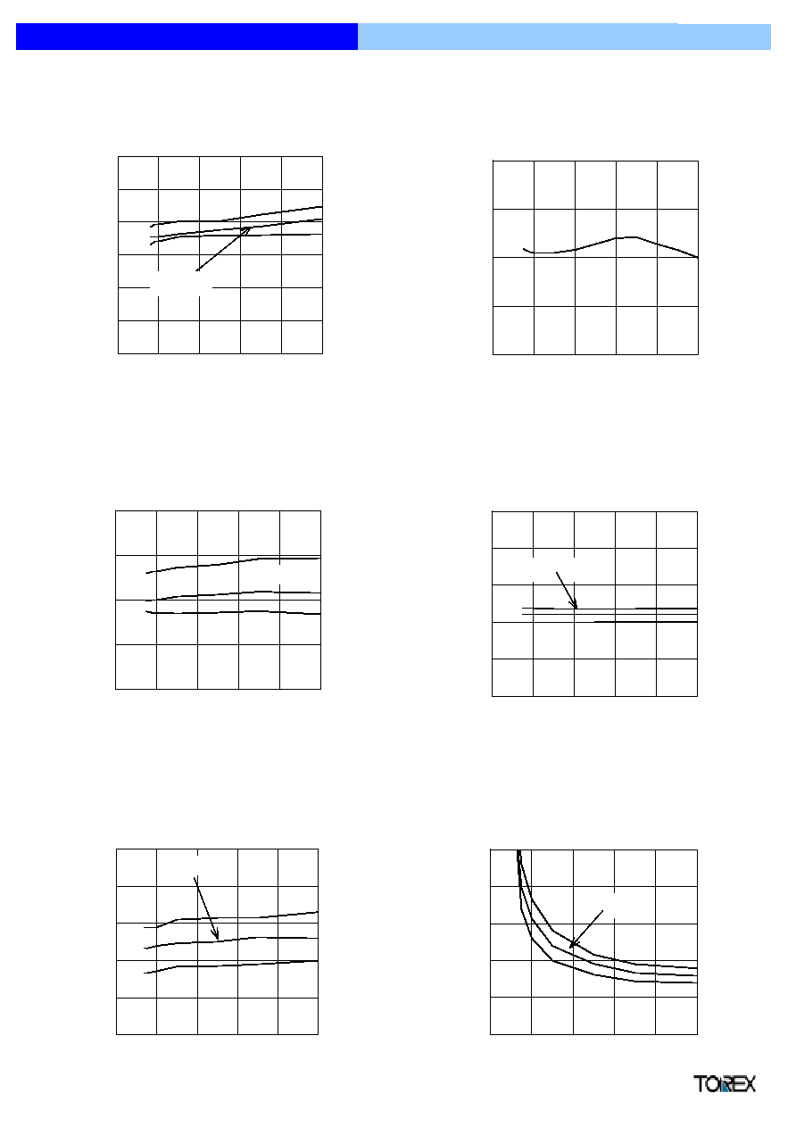
(10) PFM Duty Ratio vs. Power Supply Voltage
(11) Overcurrent SENSE Voltage vs. Power Supply Voltage
(12) Soft Start Time vs. Power Supply Voltage
(13) CE "H" "L" Voltage vs. Power Supply Voltage
(14) PWM "H" "L" Voltage vs. Power Supply Voltage
(15) EXT "H" ON Resistance vs. Power Supply Voltage
XC9103/04/05 Series
Ceramic Cap. Compatible
Step-Up DC/DC Converters
10
15
20
25
30
35
40
0
2
4
6
8
10
Supply Voltage VDD(V)
PFM Duty Ratio PFMDTY (%)
XC9105D092MR(180kHz)
85
O
C
-40
O
C
Ta=25
O
C
150
200
250
300
350
0
2
4
6
8
10
Supply Voltage VDD(V)
Ov
erc
u
rrent SENSE Voltage VLM
T
(m
V)
XC9105D092MR(180kHz)
Ta=25
O
C
0
5
10
15
20
0
2
4
6
8
10
Supply Voltage VDD(V)
Soft Start Time Tss(ms)
XC9105D092MR(180kHz)
85
O
C
-40
O
C
Ta=25
O
C
0.0
0.2
0.4
0.6
0.8
1.0
0
2
4
6
8
10
Supply Voltage VDD(V)
C
E
"H
", "L" Voltage VD
EH
, L (V)
XC9105D092MR(180kHz)
85
O
C
-40
O
C
Ta=25
O
C
-1.0
-0.8
-0.6
-0.4
-0.2
0.0
0
2
4
6
8
10
Supply Voltage VDD(V)
PWM"H
"
, "L" Voltage VPWMH
, L (V)
XC9105D092MR(180kHz)
85
O
C
-40
O
C
Ta=25
O
C
VD
D
0
10
20
30
40
50
0
2
4
6
8
10
Supply Voltage VDD(V)
EXT "
H
"
ON Res
i
s
t
anc
e REXTH (
)
XC9105D092MR(180kHz)
85
O
C
-40
O
C
Ta=25
O
C
Semiconductor Ltd.
Semiconductor Ltd.
17
(16) EXT "L" ON Resistance vs. Power Supply Voltage
(17) Operation Start Voltage vs. Ambient Temperature
(18) Operation Hold Voltage vs. Ambient Temperature
(19) Oscillation Start Voltage vs. Ambient Temperature
(20) Supply Current 1 vs. Power Supply Voltage
(21) Supply Current 2 vs. Power Supply Voltage
XC9103/04/05 Series
Ceramic Cap. Compatible
Step-Up DC/DC Converters
0
10
20
30
40
50
0
2
4
6
8
10
Supply Voltage VDD(V)
E
X
T
"L" O
N
R
e
sistance R
E
X
T
L (
)
XC9105D092MR(180kHz)
85
O
C
-40
O
C
Ta=25
O
C
0.0
0.2
0.4
0.6
0.8
1.0
1.2
-40 -20
0
20
40
60
80 100
Ambient Temperature Ta (
O
C)
O
p
eration Start Voltage VST1 (V)
IOUT=1mA
L=22
µ
H(CDRH5D28),CL=20
µ
F(ceramic)
SD:MA2Q737, Tr:2SD1628G
XC9105D092MR (180kHz,3.3V)
0.0
0.2
0.4
0.6
0.8
-40 -20
0
20
40
60
80 100
Ambient Temperature Ta (
O
C)
O
peration H
o
ld Voltage VH
LD
(V)
IOUT=1mA
L=22
µ
H(CDRH5D28), CL=20
µ
F(ceramic)
SD:MA2Q737, Tr:2SD1628G
XC9105D092MR (180kHz,3.3V)
0.0
0.2
0.4
0.6
0.8
1.0
-40 -20
0
20
40
60
80 100
Ambient Temperature Ta (
O
C)
O
scillation Start Voltage VST2 (V)
XC9105D092MR (180kHz,3.3V)
0
100
200
300
400
500
600
0
2
4
6
8
10
Supply Voltage VDD(V)
Supply C
u
rrent 1 ID
D
1
(
µ
A)
XC9105D093/095MR(300,500kHz)
500kHz
300kHz
Ta=25
O
C
0
10
20
30
40
50
0
2
4
6
8
10
Supply Voltage VDD(V)
Supply C
u
rrent 2 ID
D
2
(
µ
A)
XC9105D093/095MR(300,500kHz)
500kHz
300kHz
Ta=25
O
C
Semiconductor Ltd.
18

(22) Oscillation Frequency vs. Power Supply Voltage
(23) Maximum Duty Ratio vs. Power Supply Voltage
(24) PFM Duty Ratio vs. Power Supply Voltage
XC9103/04/05 Series
Ceramic Cap. Compatible
Step-Up DC/DC Converters
0
100
200
300
400
500
600
0
2
4
6
8
10
Supply Voltage VDD(V)
O
scillation Frequency FO
SC
(kH
z
)
XC9105D093/095MR (300,500kHz)
500kHz
300kHz
Ta=25
O
C
70
80
90
100
0
2
4
6
8
10
Supply Voltage VDD(V)
Maximum D
u
ty R
a
tio P
F
MD
TY
(
%
)
XC9105D093/095MR(300,500kHz)
500kHz
300kHz
Ta=25
O
C
10
15
20
25
30
35
40
0
2
4
6
8
10
Supply Voltage VDD(V)
PFM Duty Ratio PFMDTY (%)
XC9105D093/095MR(300,500kHz)
500kHz
300kHz
Ta=25
O
C
Semiconductor Ltd.
19