1
XC9119D10A ETR0408_003
GENERAL DESCRIPTION
The XC9119D01A series is 1MHz, PWM controlled step-up
DC/DC converter, designed to allow the use of ceramic
capacitors. With a built-in 2.0
switching transistor, the
XC9119D01A series can easily provide a step-up operation
by using only a coil, a diode, a capacitor, and a resistor,
connected externally.
Since output voltage up to 19.5V (Maximum Lx operating
voltage: 20V) can be derived with reference voltage supply of
1.0V (±2.0%) and external components, the series can easily
supply high voltage for various general-purpose power
supplies, LCD panels and organic EL displays.
With a high switching frequency of 1.0MHz, a low profile and
small board area solution can be achieved using a chip coil
and an ultra small ceramic output capacitor.
With the current limit function (400mA (TYP.): V
DD
=3.6V), a
peak current, which flows through built-in driver transistors
can be limited.
Soft-start time can be adjusted by external
resistors and capacitors. The stand-by function enables the
output to be turned off (CE 'L'), that is, the supply current will
be less than 1.0
µA.
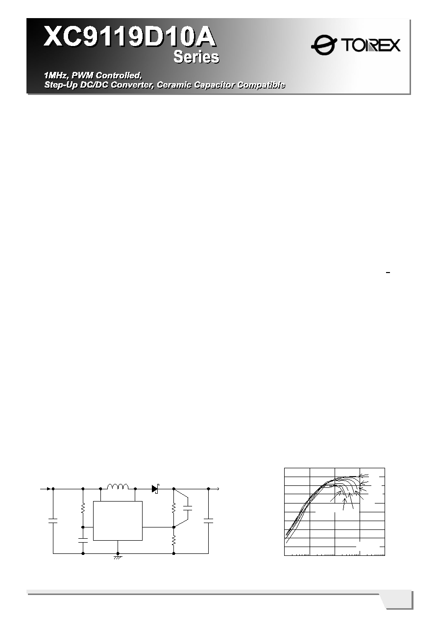
TYPICAL APPLICATION CIRCUIT
APPLICATIONS
Organic electroluminescene display (OELD)
Power supplies for LCD panels
Various general-purpose power supplies
FEATURES
Operating Voltage Range: 2.5V ~ 6.0V
Output Voltage Range : Up to 19.5V externally set-up
: Reference voltage 1.0V +2.0%
Oscillation Frequency : 1.0MHz±20%
ON Resistance :
2.0
(V
DD
: 3.6V, V
DS
: 0.4V)
Efficiency :
86%
(V
OUT
=15V, V
DD
=3.6V, I
OUT
=10mA)
Control
: PWM control
Stand-by function :
ISTB=1.0
µA (MAX.)
Load Capacitor
: Low ESR cap. such as a
ceramic capacitor compatible
Lx Limit Current
: 400mA (V
DD
:3.6V)
Operating Voltage Range : 2.5V ~ 6.0V
Output Voltage Externally Set-Up
: Vref =1.0V ± 2.0%
(Can be set freely up to 19.5V)
Oscillation Frequency
: 1.0MHz (Accuracy ± 20%)
High Efficiency
: 86%
(V
DD
=3.6V, V
OUT
=15V, I
OUT
=10mA)
Ultra Small Packages
: SOT-25, USP-6C
TYPICAL PERFORMANCE
CHARACTERISTICS
Efficiency vs. Output Current
0
10
20
30
40
50
60
70
80
90
100
0.1
1
10
100
1000
Output Current: I
OUT
(mA)
Ef
f
i
ci
e
n
cy:
EF
F
I
(
%
)
6V
5V
4.2V
3.6V
3V
2.7V
VIN=2.5V
T a=25
o
C
XC9119D10A
VDD
Lx
CE/SS
FB
VSS
L:22uH
CDRH4D18C
VIN
CL
10uF
SD
XB01SB04A2BR
RFB2
36k
CIN
4.7uF
RFB1
510k
C FB
620pF
RSS
220k
CSS
0.1uF
VOUT=15V
(up to 19.5V)
2
XC9119D10A
Series
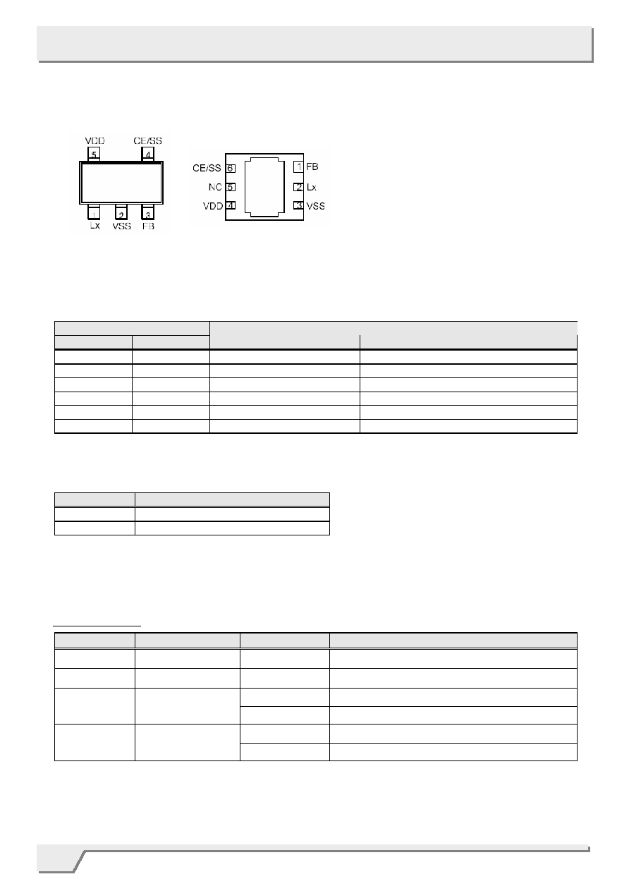
PIN NUMBER
SOT-25
USP-6C
PIN NAME
FUNCTION
1 2
Lx
Switch
2 3
V
SS
Ground
3 1
FB
Voltage
Feedback
4
6
CE/SS
Chip Enable/ Soft Start
5 4
V
DD
Power
Input
- 5
NC
No
Connection
DESIGNATOR
DESCRIPTION
SYMBOL
DESCRIPTION
12
Output Voltage
10
: FB voltage
3
Oscillation Frequency
A
: 1MHz
M :
SOT-25
4
Package
E :
USP-6C
R
: Embossed tape, standard feed
5
Device Orientation
L
: Embossed tape, reverse feed
CE/SS PIN
OPERATIONAL STATE
H Operation
L Shut-down
PIN CONFIGURATION
SOT-25
(TOP VIEW)
USP-6C
(BOTTOM VIEW)
PIN ASSIGNMENT
CE PIN FUNCTION
PRODUCT CLASSIFICATION
Ordering Information
XC9119D
12345
*The dissipation pad for the USP-6C
package should be solder-plated in
recommended mount pattern and metal
masking so as to enhance mounting
strength and heat resistance. If the pad
needs to be connected to other pins, it
should be connected to the V
SS
pin.

4
XC9119D10A
Series
MARK
PRODUCT SERIES
XC9119xxxxMx
MARK
Lx OVERVOLTAGE LIMIT
PRODUCT SERIES
D Not
Available
XC9119DxxxMx
MARK
OSCILLATION FREQUENCY
PRODUCT SERIES
A 1MHz
XC9119xxxAMx
MARK
PRODUCT SERIES
V XC9119xxxxDx
MARK
Lx OVERVOLTAGE LIMIT
PRODUCT SERIES
D Not
Available
XC9119DxxxDx
MARK
FB VOLTAGE (V)
PRODUCT SERIES
1 0
1.0
XC9119x10xDx
MARK
OSCILLATION FREQUENCY
PRODUCT SERIES
A 1MHz
XC9119xxxADx
MARKING RULE
Represents product series
SOT-25
Represents Lx overvoltage limit
Represents oscillation frequency
Represents production lot number
0 to 9 and A to Z, or inverted characters 0 to 9 and A to Z repeated.
(G, I, J, O, Q, W excepted)
USP-6C
Represents product series
Represents Lx overvoltage limit
Represents FB voltage
Represents oscillation frequency
Represents production lot number
0 to 9 and A to Z repeated (G, I, J, O, Q, W excepted)
* No character inversion used.
L
SOT-25
(TOP VIEW)
USP-6C
(TOP VIEW)