
PWM Controlled Step-Down DC/DC Converters
Series
535
5
The XC9201 series are step-up multiple current and voltage feedback
DC/DC controller ICs. Current sense, clock frequencies and amp
feedback gain can all be externally regulated.
A stable power supply is possible with output currents of up to 3.0A.With
output voltage fixed internally, V
OUT
is selectable in 0.1V steps within a
1.2V - 16.0V range (± 2.5%).
For output voltages outside this range, we recommend the FB version
which has a 0.9V internal reference voltage. Using this version, the
required output voltage can be set-up using 2 external resistors.
Switching frequencies can also be set-up externally within a range of
100~600 kHz and therefore frequencies suited to your particular
application can be selected.
With the current sense function, peak currents (which flow through the
driver transistor and the coil) can be controlled. Soft-start time can be
adjusted using external resistors and capacitors.
During shutdown (CE pin =L), consumption current can be reduced to as
little as 0.5
µA (TYP.) or less and with U.V.L.O
(Under Voltage Lock Out) built-in, the external transistor will be
automatically shut off below the regulated voltage.
General Description
GStable Operations via Current & Voltage Multiple Feedback
GUnlimited Options for Peripheral Selection
GCurrent Protection Circuit
GCeramic Capacitor Compatible
GMobile, Cordless phones
GPalm top computers, PDAs
GPortable games
GCameras, Digital cameras
GLaptops
Features
Applications
NInput Voltage Range
: 2.5V ~20V
NOutput Voltage Range
: 1.2V ~ 16V
NOscillation Frequency Range : 100kHz ~
600kHz
NOutput Current
: up to 3.0A
NCeramic Capacitor Compatible
NMSOP-8A Package
0
20
40
60
80
100
0.1
1
10
100
1000
10000
Output CurrentI
OUT
mA
EfficiencyEFFI (%)
7.2V
15.0V
V
IN
=5.4V
10.0V
12.0V
22H
10K
220pF
CLK 5
1 EXT
2 Isen
3 V
IN
4 CE/SS
V
OUT
7
GAIN 6
Vss 8
470pF
40F+220F
33m
XP132A11A1SR
U3FWJ44N
1F
240k
0.33F
94F
Typical Application Circuit
Typical Performance
Characteristic
V
OUT
:5.0V FOSC:330kHz
05S_1XC9201/9202 02.09.12 15:16 535
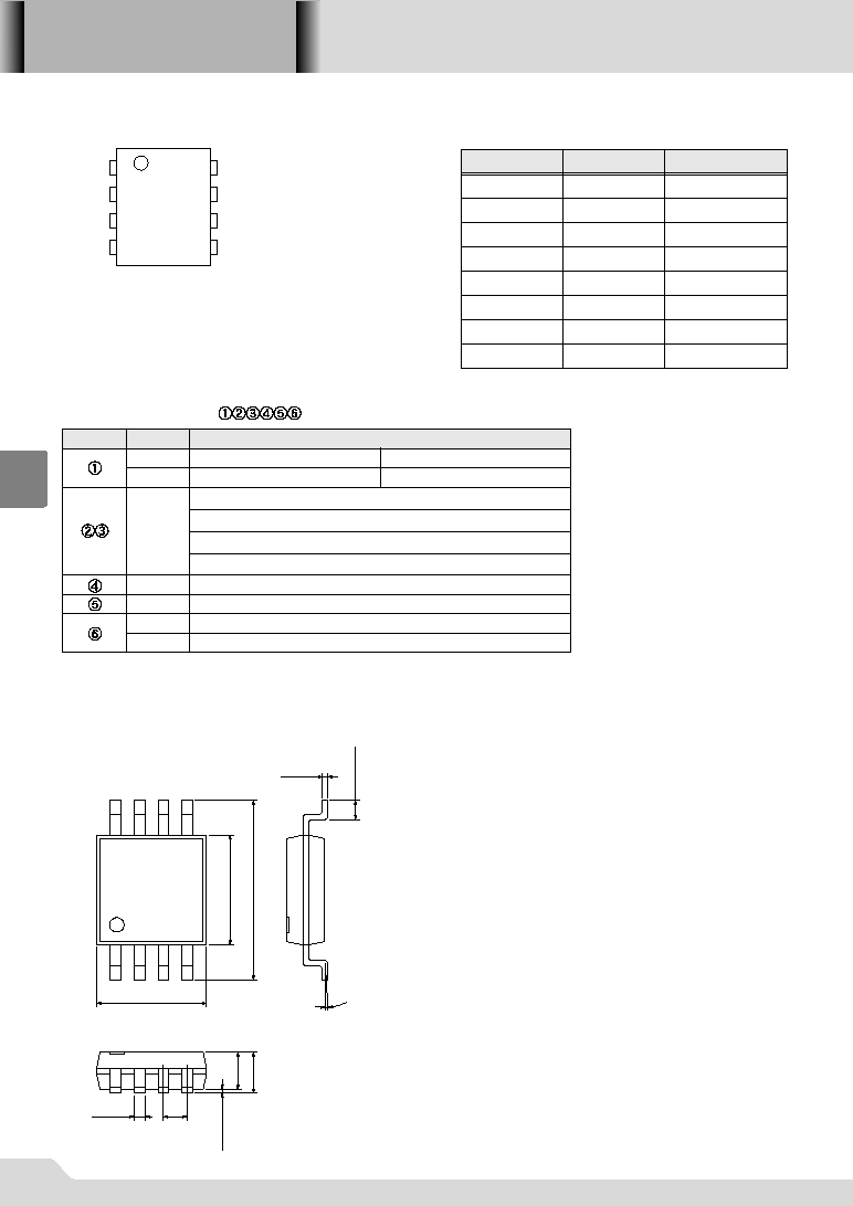
Packaging Information
GMSOP-8A
XC9201
Series
536
5
Pin Configuration
Pin Assignment
Product Classification
GOrdering Information
1
2
3
4
6
5
7
8
EXT
Isen
V
IN
CESS
CCGAIN
CLK
V
OUT
FB
V
SS
PIN NUMBER
PIN NAME
FUNCTION
1
EXT
Driver
2
Isen
Current Sense
3
V
IN
Power Input
4
CESS
CE/Soft Start
5
CLK
Clock Input
6
CCGAIN
Phase Compensation
7
V
OUT
FB
Voltage Sense
8
V
SS
Ground
DESIGNATOR SYMBOL
DESCRIPTION
C
V
OUT
D
Number
FB
A
K
R
Embossed tape. Standard Feed
Embossed tape. Reverse Feed
L
Output Voltage : For voltages above 10V, see below :
10=A, 11=B, 12=C, 13=D, 14=E, 15=F, 16=H
e.g. V
OUT
=2.3V
w=2, e=3 V
OUT
=13.5V
w=D, e=5
FB products
w=0, e=9 fixed
Soft-start externally set-up
Soft-start externally set-up
MSOP-8A
Adjustable Frequency
The standard output voltages of the XC9201C series are 2.5V, 3.3V, and 5.0V.
Voltages other than those listed are semi-custom.
3.00±0.10
4.90±0.10
3.00±0.10
0.53±0.13
0 6
0.000.20
0.30
+0.08
-0.02
1.02
0.86
+0.11 -0.10
+0.20 -0.21
0.15
+0.08
-0.02
(0.65)
05S_1XC9201/9202 02.09.12 15:16 536

XC9201
Series
537
5
Marking
qRepresents the product series
SYMBOL
1
PRODUCT NAME
XC9201***AK*
wRepresents the product type, DC/DC converter
SYMBOL
C
PRODUCT NAME
D
TYPE
V
OUT
CE PIN
FBCE PIN
eRepresents integral number of output voltage,or FB type
SYMBOL
1
PRODUCT NAME
2
VOLTAGE
1. X
2. X
3
3. X
4
4. X
5
5. X
6
6. X
7
7. X
8
8. X
9
9. X
0
FB products
SYMBOL
A
PRODUCT NAME
B
VOLTAGE
10. X
11. X
C
12. X
D
13. X
E
14. X
F
15. X
H
16. X
rRepresents decimal number of output voltage
SYMBOL
0
PRODUCT NAME
3
VOLTAGE
X. 0
X. 3
9
FB products
tRepresents oscillator frequeney's control type
SYMBOL
A
PRODUCT NAME
XC9201***AK*
TYPE
Adjustable Frequency
MSOP8A
q w e
r t y
XC9201C**AK*
XC9201D09AK*
XC9201C1*AK*
XC9201C2*AK*
XC9201C3*AK*
XC9201C4*AK*
XC9201C5*AK*
XC9201C6*AK*
XC9201C7*AK*
XC9201C8*AK*
XC9201C9*AK*
XC9201D09AK*
XC9201CA*AK*
XC9201CB*AK*
XC9201CC*AK*
XC9201CD*AK*
XC9201CE*AK*
XC9201CF*AK*
XC9201CH*AK*
XC9201C*0AK*
XC9201C*3AK*
XC9201D09AK*
05S_1XC9201/9202 02.09.12 15:16 537
XC9201
Series
538
5
Absolute Maximum Ratings
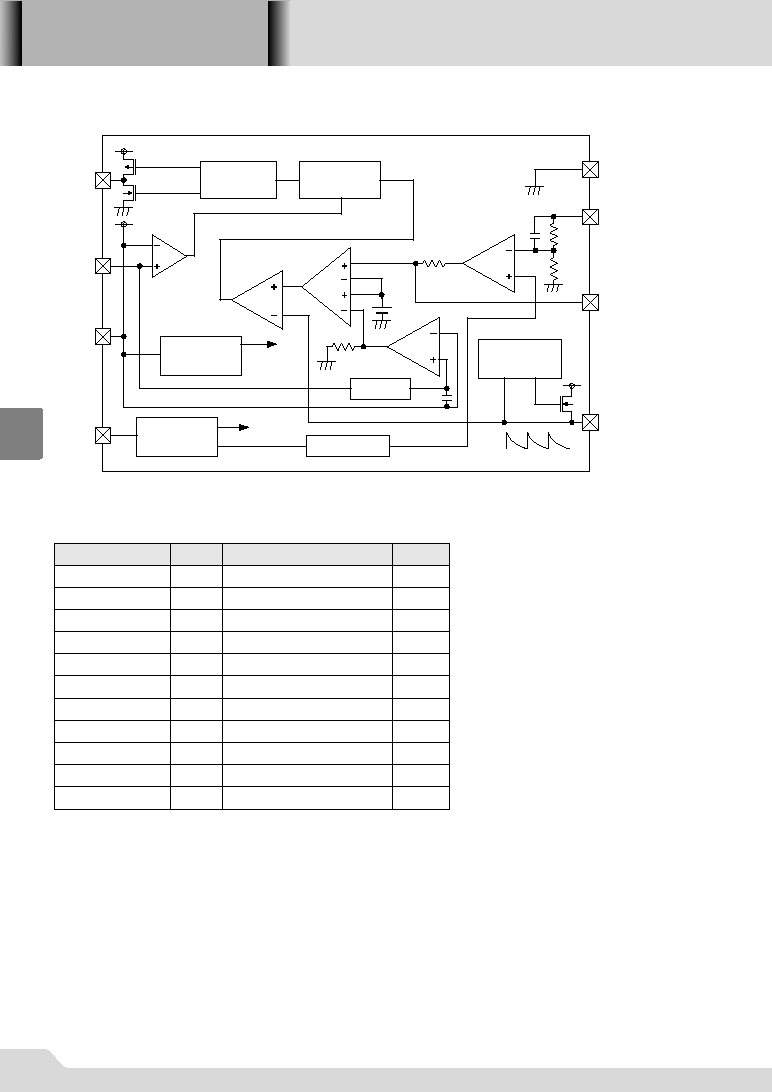
Block Diagram
EXT
ISEN
V
IN
CE/SS
V
SS
V
OUT
CC/GAIN
CLK
Ramp Wave,
Internal CLK
generator
Chip Enable,
Soft Start up,
U.V.L.O.
Verr
PWM
Ierr
Internal
Voltage
Regulator
EXT timming
controll
logic
Current
Limit
Protection
Limitter comp.
Vref generator
CE,UVLO
to internal
circuit
0.9V
Sampling
R1
R2
MIX
2.0V
to internal
circuit
PARAMETER
EXT Pin Voltage
SYMBOL
R A T I N G S
UNITS
-0.322
ISEN Pin Voltage
V
IN
Pin Voltage
CE/SS Pin Voltage
CLK Pin Voltage
V
OUT
/FB Pin Voltage
EXT Pin Current
Storage Temperature
V
EXT
VIsen
V
IN
V
CE
V
CLK
V
OUT
/FB
I
EXT
Tstg
-0.3V
DD
0.3
-0.322
-0.322
-0.3V
DD
0.3
-0.322
±100
-55125
mA
Continuous Total
Power Dissipation
Pd
150
mW
Operating Ambient
Temperature
Topr
-4085
Ta=25
CC/GAIN Pin Voltage
V
CC
-0.3V
DD
0.3
05S_1XC9201/9202 02.09.12 15:16 538

XC9201
Series
539
5
Electrical Characteristics
XC9201C25AR
V
IN
= 3.75V unless specified
*1 : On resistance = 0.4V / measurement current
NOTE1 : EFFI = {[(Output Voltage) x (Output Current)]
˜ [(Input Voltage) x (Input Current)]} x 100
NOTE2 : The capacity range of the condenser used to set the external CLK frequency is 180
300pF
Ta=25
PARAMETER
SYMBOL
CONDITIONS
MIN.
TYP.
MAX.
UNITS
Maximum Operating
Voltage
Minimum Operating
Voltage
CLK Oscillation
Frequency
Supply Current 1
Stand-by Current
Frequency Temperature
Fluctuation
Maximum Duty Cycle
Minimum Duty Cycle
V
IN
max
Output Voltage
V
OUT
V
IN
min
I
DD
1
I
STB
F
OSC
Frequency Input
Stability
F
OSC
V
IN
F
OSC
F
OSC
T
OPR
F
OSC
MAXDTY
MINDTY
Current Limiter Voltage
I
SEN
Current
I
LIM
I
ISEN
CE "High" Current
CE "Low" Current
I
CEH
I
CEL
CE "High" Voltage
V
CEH
EXT voltage = High
V
IN
=3.75V, CE=V
IN
=V
OUT
V
IN
=20.0V, CE=V
IN
, V
OUT
=V
SS
V
IN
=3.75V, CE=V
OUT
=V
SS
RT=10.0k, CT=220pF
V
IN
=2.5V20V
TOPR=-40+85
V
IN
=3.75V
I
OUT
=300mA
V
OUT
=V
SS
V
OUT
=V
IN
V
IN
pin voltage - I
SEN
pin voltage
V
IN
=3.75V, I
SEN
=3.75V
CE=V
IN
=20.0V, V
OUT
=0V
CE=0V, V
IN
=20.0V, V
OUT
=0V
Existance of CLK Oscillation,
V
OUT
=0V, CEVoltage applied
Dissapearance of CLK Oscillation,
V
OUT
=0V, CEVoltage applied
EXT=V
IN
-0.4V, CE=V
OUT
=V
IN
*1
EXT=0.4V, CE=V
IN
, V
OUT
=V
SS
*1
Connect C
SS
and R
SS
, CE : 0V
3.75V
2.438
20
-
1.0
280
100
90
4.5
-0.1
-0.1
0.6
2.500
-
-
1.400
115
130
0.5
330
±5
±5
150
7
0
0
2.562
-
2.200
2.0
220
235
2.0
380
0
220
13
0.1
0.1
V
V
V
V
A
A
A
kHz
%
%
%
%
mV
A
A
A
V
CE "Low" Voltage
V
CEL
0.2
V
EXT "High"
ON Resistance
R
EXTH
27
40
EXT "Low"
ON Resistance
R
EXTL
24
33
Efficiency
(NOTE1)
EFFI
93
%
Soft-start Time
T
SS
5
10
20
ms
CC/GAIN Pin
Output Impedance
R
CCGAIN
400
k
CIRCUITS
q
q
q
t
w
w
w
e
e
e
r
r
y
y
t
t
t
t
r
r
q
q
u
Supply Current 2
I
DD
2
U.V.L.O. Voltage
V
UVLO
05S_1XC9201/9202 02.09.12 15:16 539

XC9201
Series
540
5
XC9201C33AR
V
IN
= 5.0V unless specified
*1 : On resistance = 0.4V / measurement current
NOTE1 : EFFI = {[(Output Voltage) x (Output Current)]
˜ [(Input Voltage) x (Input Current)]} x 100
NOTE2 : The capacity range of the condenser used to set the external CLK frequency is 180
300pF
Ta=25
PARAMETER
SYMBOL
CONDITIONS
UNITS
Maximum Operating
Voltage
Minimum Operating
Voltage
Supply Current 1
Stand-by Current
Frequency Temperature
Fluctuation
Maximum Duty Cycle
Minimum Duty Cycle
V
IN
max
Output Voltage
V
OUT
V
IN
min
I
DD
1
I
STB
CLK Oscillation
Frequency
F
OSC
Frequency
Input Stability
F
OSC
V
IN
F
OSC
F
OSC
T
OPR
F
OSC
MAXDTY
MINDTY
Current Limiter
Voltage
I
SEN
Current
I
LIM
I
ISEN
CE "High" Current
CE "Low" Current
I
CEH
I
CEL
CE "High" Voltage
V
CEH
EXT voltage = High
V
IN
=5.0V, CE=V
IN
=V
OUT
V
IN
=20.0V, CE=V
IN
, V
OUT
=V
SS
V
IN
=5.0V, CE=V
OUT
=V
SS
RT=10.0k, CT=220pF
V
IN
=2.5V20V
Topr=-40+85
V
IN
=5.0V
I
OUT
=300mA
V
OUT
=V
SS
V
OUT
=V
IN
V
IN
pin voltage - I
SEN
pin voltage
V
IN
=5.0V, I
SEN
=5.0V
CE=V
IN
=20.0V, V
OUT
=0V
CE=0V, V
IN
=20.0V, V
OUT
=0V
Existance of CLK Oscillation,
V
OUT
= 0V, CE : Voltage applied
Dissapearance of CLK Oscillation,
V
OUT
= 0V, CE : Voltage applied
EXT=V
IN
- 0.4V, CE=V
OUT
=V
IN
*1
EXT=0.4V, CE=V
IN
, V
OUT
=VSS *1
Connect C
SS
and R
SS
, CE : 0V 5.0V
3.218
20
-
1.0
280
100
90
4.5
-0.1
-0.1
0.6
3.300
-
-
1.400
115
130
0.5
330
±5
±5
150
7
0
0
3.382
-
2.200
2.0
220
235
2.0
380
0
220
13
0.1
0.1
V
V
V
V
A
A
A
kHz
%
%
%
%
mV
A
A
A
V
CE "Low" Voltage
V
CEL
0.2
V
EXT "High"
ON Resistance
EXT "Low"
ON Resistance
CC/GAIN Pin
Output Impedance
R
EXTH
24
33
R
EXTL
22
31
Efficiency
(NOTE1)
EFFI
93
%
Soft-start Time
T
SS
5
10
20
ms
R
CCGAIN
400
k
CIRCUITS
q
q
q
t
w
w
w
e
e
e
r
r
y
y
t
t
t
t
r
r
q
q
u
Supply Current 2
I
DD
2
U.V.L.O. Voltage
V
UVLO
MIN.
TYP.
MAX.
05S_1XC9201/9202 02.09.12 15:16 540

XC9201
Series
541
5
XC9201C50AR
V
IN
= 7.5V unless specified
*1 : On resistance = 0.4V / measurement current
NOTE1 : EFFI = {[(Output Voltage) x (Output Current)]
˜ [(Input Voltage) x (Input Current)]} x 100
NOTE2 : The capacity range of the condenser used to set the external CLK frequency is 180
300pF
Ta=25
V
IN
max
V
OUT
V
IN
min
I
DD
1
I
STB
F
OSC
F
OSC
V
IN
F
OSC
F
OSC
T
OPR
F
OSC
MAXDTY
MINDTY
I
LIM
I
ISEN
I
CEH
I
CEL
V
CEH
EXT voltage = High
V
IN
=7.5V, CE=V
IN
=V
OUT
V
IN
=20.0V, CE=V
IN
, V
OUT
=V
SS
V
IN
=7.5V, CE=V
OUT
=V
SS
RT=10.0k, CT=220pF
V
IN
=2.5V20V
TOPR=-40+85
V
IN
=7.5V
I
OUT
=300mA
V
OUT
=V
SS
V
OUT
=V
IN
V
IN
pin voltage - I
SEN
pin voltage
V
IN
=7.5V, I
SEN
=7.5V
CE=V
IN
=20.0V, V
OUT
=0V
CE=0V, V
IN
=20.0V, V
OUT
=0V
Existance of CLK Oscillation,
V
OUT
=0V, CEVoltage applied
Dissapearance of CLK Oscillation,
V
OUT
=0VCEVoltage applied
VEXT=V
IN
-0.4V, CE=V
OUT
=V
IN
*1
VEXT=0.4V, CE=V
IN
, V
OUT
=V
SS
*1
Connect C
SS
and R
SS
, CE : 0V 7.5V
4.875
20
-
1.0
280
100
90
4.5
-0.1
-0.1
0.6
5.000
-
-
1.400
115
130
0.5
330
±5
±5
150
7
0
0
5.125
-
2.200
2.0
220
235
2.0
380
0
220
13
0.1
0.1
V
V
V
V
A
A
A
kHz
%
%
%
%
mV
A
A
A
V
V
CEL
0.2
V
R
EXTH
21
29
R
EXTL
20
27
EFFI
93
%
T
SS
5
10
20
ms
R
CCGAIN
400
k
q
q
q
t
w
w
w
e
e
e
r
r
y
y
t
t
t
t
r
r
q
q
u
I
DD
2
V
UVLO
MIN.
TYP.
MAX.
PARAMETER
Minimum Operating
Voltage
Maximum Operating
Voltage
Supply Current 1
Stand-by Current
Minimum Duty Cycle
Output Voltage
CLK Oscillation
Frequency
Frequency
Input Stability
Current Limiter
Voltage
I
SEN
Current
CE "High" Voltage
CE "Low" Voltage
CE "High" Voltage
CE "Low" Voltage
EXT "High"
ON Resistance
EXT "Low"
ON Resistance
CC/GAIN Pin
Output Impedance
Efficiency
(NOTE1)
Soft-start Time
Supply Current 2
U.V.L.O. Voltage
SYMBOL
CONDITIONS
UNITS CIRCUITS
Frequency Temperature
Fluctuation
Maximum Duty Cycle
05S_1XC9201/9202 02.09.12 15:16 541
XC9201
Series
542
5
XC9201D09AR
V
IN
= 4.0V unless specified
External components : RFB1 = 200k
, RFB2 = 100k, CFB = 82pF
*1 : On resistance = 0.4V / measurement current
NOTE1 : EFFI = {[(Output Voltage) x (Output Current)]
˜ [(Input Voltage) x (Input Current)]} x 100
NOTE2 : The capacity range of the condenser used to set the external CLK frequency is 180
300pF
Ta=25
UNITS
V
IN
max
V
FB
V
IN
min
I
DD
1
I
STB
F
OSC
F
OSC
V
IN
F
OSC
F
OSC
T
OPR
F
OSC
MAXDTY
MINDTY
I
LIM
I
ISEN
I
CEH
I
CEL
V
CEH
EXT voltage = High
V
IN
=4.0V, CE=V
IN
=FB
V
IN
=20.0V, CE=V
IN
, FB=V
SS
V
IN
=4.0V, CE=FB=V
SS
RT=10.0k, CT=220pF
V
IN
=2.5V20V
TOPR=-40+85
V
IN
=4.0V
I
OUT
=300mA
FB=V
SS
FB=V
IN
V
IN
pin voltage - I
SEN
pin voltage
V
IN
=4.0V, I
SEN
=4.0V
CE=V
IN
=20.0V, FB=0V
CE=0V, V
IN
=20.0V, FB=0V
Existance of CLK Oscillation,
FB=0V, CEVoltage applied
Dissapearance of CLK Oscillation,
FB=0VCEVoltage applied
EXT=V
IN
-0.4V, CE=FB=V
IN
*1
EXT=0.4V, CE=V
IN
, FB=V
SS
*1
Connect C
SS
and R
SS
, CE : 0V 4.0V
0.8775
20
1.0
280
100
90
4.5
-0.1
-0.1
0.6
0.900
1.400
115
130
0.5
330
±5
±5
150
7
0
0
0.9225
2.200
2.0
220
235
2.0
380
0
220
13
0.1
0.1
V
V
V
V
A
A
A
kHz
%
%
%
%
mV
A
A
A
V
V
CEL
0.2
V
R
EXTH
27
40
R
EXTL
24
34
EFFI
93
%
T
SS
5
10
20
ms
R
CCGAIN
400
k
CIRCUITS
q
q
q
t
w
w
w
e
e
e
r
r
y
y
t
t
t
t
r
r
q
q
u
I
DD
2
V
UVLO
MIN.
TYP.
MAX.
PARAMETER
SYMBOL
CONDITIONS
Maximum Operating
Voltage
Minimum Operating
Voltage
Supply Current 1
Stand-by Current
Frequency Temperature
Fluctuation
Maximum Duty Cycle
Minimum Duty Cycle
FB Voltage
CLK Oscillation
Frequency
Frequency
Input Stability
Current Limiter
Voltage
I
SEN
Current
CE "High" Current
CE "Low" Current
CE "High" Voltage
CE "Low" Voltage
EXT "High"
ON Resistance
EXT "Low"
ON Resistance
CC/GAIN Pin
Output Impedance
Efficiency
(NOTE1)
Soft-start Time
Supply Current 2
U.V.L.O. Voltage
05S_1XC9201/9202 02.09.12 15:16 542

XC9201
Series
543
5
3.3V
1.5A
47F(OS) or
10F(ceramic)◊4
V
SS
V
OUT
CC/GAIN
30k
220pF
470pF
CLK
8
7
6
5
22H
1
EXT
Isen
2
3
V
IN
4
CE/SS
1F
SD
47
7.2V
50m
PMOS
240k
F 0.22F
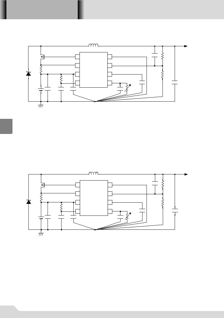
Typical Application Circuits
XC9201C33AKR
5.0V
1.5A
47F(OS)
+220F(any)
V
SS
V
OUT
CC/GAIN
30k
220pF
470pF
CLK
8
7
6
5
22H
1
EXT
Isen
2
3
V
IN
4
CE/SS
1F
SD
12.0V
20m
PMOS
240k
0.33F
47F
+220F
PMOS
: XP132A11A1SR(TOREX)
Coil
: 22
µH(CR105 SUMIDA)
Resistor
: 50m
for Isen (NPR1 KOWA), 30k(trimmer) for CLK, 240k for SS
Capacitors : 220pF( ceramic) for CLK, 470pF(ceramic) for CC/GAIN, 0.22
µF(any) for SS,1µF(ceramic) for Bypass
47
µF(OS) or 10µF(ceramic) x 4 for C
L
, 47
µF(tantalum) for C
IN
SD
: U3FWJ44N(TOSHIBA)
XC9201C50AKR
PMOS
: XP132A11A1SR(TOREX)
Coil
: 22
µH(CDRH127 SUMIDA)
Resistor
: 20m
for Isen (NPR1 KOWA), 30k(trimmer) for CLK, 240k for SS
Capacitors : 220pF(ceramic) for CLK, 470pF(ceramic) for CC/GAIN, 0.33
µF(any) for SS, 1µF(ceramic) for Bypass
47
µF(OS)+220µF(any) for C
L
, 47
µF(tantalum)+220µF(any) for C
IN
SD
: U3FWJ44N(TOSHIBA)
05S_1XC9201/9202 02.09.12 15:16 543
XC9201
Series
544
5
2.5V
3A
47uF(OS)
+220F(any)
V
SS
V
OUT
CC/GAIN
30k
220k
220pF
39pF
470pF
CLK
8
7
6
5
22H
1
EXT
Isen
2
3
V
IN
4
CE/SS
1F
SD
7.2V
20m
PMOS
240k
390k
0.22F
47F
+220F
12V
1.5A
47F(OS)
+220F
V
SS
FB
CC/GAIN
30k
22k
220pF
56pF
470pF
CLK
8
7
6
5
47H
1
EXT
Isen
2
3
V
IN
4
CE/SS
XC9201D09AKR
1F
SD
20V
50m
PMOS
240k
270k
0.47F
47F
XC9201D09AKR
PMOS
: XP132A11A1SR(TOREX)
Coil
: 22
µH(CDRH127 SUMIDA)
Resistors
: 20m
for Isen (NPR1 KOWA), 30k(trimmer) for CLK, 240k for SS, 390k for Output Voltage
100k
(trimmer) for Output Voltage
Capacitors : 220pF(ceramic) for CLK, 470pF(ceramic) for CC/GAIN, 0.22
µF(any) for SS, 1µF(ceramic) for Bypass
39pF(ceramic) for FB,47
µF(OS) for C
L
,47
µF (tantalum)+220µF(any) for C
IN
SD
: U3FWJ44N(TOSHIBA)
PMOS
: XP132A11A1SR(TOREX)
Coil
: 47
µH(CR105 SUMIDA)
Resistor
: 50m
for Isen (NPR1 KOWA), 30k(trimmer) for CLK, 240k for SS, 270k for Output Voltage
22k
(trimmer) for Output Voltage
Capacitors : 220pF(ceramic) for CLK, 470pF(ceramic) for CC/GAIN, 0.47
µF(any) for SS, 1µF(ceramic) for Bypass
100pF(ceramic) for FB, 47
µF(OS) +220µF(any) for C
L
, 47
µF(tantalum)+220µF(any) for C
IN
SD
: U3FWJ44N(TOSHIBA)
05S_1XC9201/9202 02.09.12 15:16 544
XC9201
Series
545
5
D
CLK
Q
/RESET
PWM/PFM switching signal
CLK sync signal
Output signal to EXT pin
Limiter signal
PWM/PFM switchinig signal
Operation Description
Step-down DC/DC converter controllers of the XC9201series carry out pulse width modulation (PWM) according to the multiple feedback signals
of the output voltage and coil current.
The internal circuits consist of different blocks that operate at V
IN
or the stabilized power (2.0 V) of the internal regulator. The output setting
voltage of type C controller and the FB pin voltage (Vref = 0.9 V) of type D controller have been adjusted and set by laser-trimming.
<Clock>
With regard to clock pulses, a capacitor and resistor connected to the CLK pin generate ramp waveforms whose top and bottom are 0.7 V and
0.15 V, respectively. The frequency can be set within a range of 100 to 600 kHz externally (refer to the "Functional Settings" section for further
information). The clock pulses are processed to generate a signal used for synchronizing internal sequence circuits.
<Verr amplifier>
The Verr amplifier is designed to monitor the output voltage. A fraction of the voltage applied to internal resistors R1, R2 in the case of a type C
controller, and the voltage of the FB pin in the case of a type D controller, are fed back and compared with the reference voltage. In response to
feedback of a voltage lower than the reference voltage, the output voltage of the Verr amplifier increases.
The output of the Verr amplifier enters the mixer via resistor (RVerr). This signal works as a pulse width control signal during PWM operations.
By connecting an external capacitor and resistor through the CE/GAIN pin, it is possible to set the gain and frequency characteristics of Verr
amplifier signals (refer to the "Functional Settings" section for further information).
<Ierr amplifier>
The Ierr amplifier monitors the coil current. The potential difference between the V
IN
and Isen pins is sampled at each switching operation.
Then the potential difference is amplified or held, as necessary, and input to the mixer. The Ierr amplifier outputs a signal ensuring that the
greater the potential difference between the V
IN
and Isen pins, the smaller the switching current. The gain and frequency characteristics of this
amplifier are fixed internally.
<Mixer and PWM>
The mixer modulates the signal sent from Verr by the signal from Ierr. The modulated signal enters the PWM comparator for comparison with
the sawtooth pulses generated at the CLK pin. If the signal is greater than the sawtooth waveforms, a signal is sent to the output circuit to turn
on the external switch.
<Current Limiter>
The current flowing through the coil is monitored by the limiter comparator via the V
IN
and Isen pins. The limiter comparator outputs a signal
when the potential difference between the V
IN
and Isen pins reaches 150 mV or more. This signal is converted to a logic signal and handled as
a DFF reset signal for the internal limiter circuit. When a reset signal is input, a signal is output immediately at the EXT pin to turn off the MOS
switch. When the limiter comparator sends a signal to enable data acceptance, a signal to turn on the MOS switch is output at the next clock
pulse. If at this time the potential difference between the V
IN
and Isen pins is large, operation is repeated to turn off the MOS switch again. DFF
operates in synchronization with the clock signal of the CLK pin.
<Soft Start>
The soft start function is made available by attaching a capacitor and resistor to the CE/SS pin. The Vref voltage applied to the Verr amplifier is
restricted by the start-up voltage of the CE/SS pin. This ensures that the Verr amplifier operates with its two inputs in balance, thereby
preventing the ON-TIME signal from becoming stronger than necessary. Consequently, soft start time needs to be set sufficiently longer than
the time set to CLK. The start-up time of the CE/SS pin equals the time set for soft start (refer to the "Functional Settings" section for further
information).
The soft start function operates when the voltage at the CE/SS pin is between 0V to 1.55V. If the voltage at the CE/SS pin doesn't start from 0V
but from a mid level voltage when the power is switched on, the soft start function will become ineffective and the possibilities of large inrush
currents and ripple voltages occurring will be increased.
Undervoltage Lock Out (U.V.L.O.) is also provided. This function is activated to turn off the MOS switch attached to the EXT pin when the input
voltage (V
IN
) decreases to approximately 1.4 V or below. The purpose of this function is to keep the external MOS switch from turning on when
a voltage at which the IC operates unstably is applied. U.V.L.O. also restricts signals during soft start so that the external MOS switch does not
turn on until the internal circuitry becomes stable.
05S_1XC9201/9202 02.09.12 15:16 545
GFunctional Settings
1. Soft Start
CE and soft start (SS) functions are commonly assigned to the CE/SS pin. The soft start function is effective until the voltage at the CE pin
reaches approximately 1.55 V rising from 0 V. Soft start time is approximated by the equation below according to values of Vcont, R
SS
, and
C
SS
.
T=-Css x Rss x ln((Vcont-1.55)/Vcont)
Example: When Css=0.1
µF,Rss=470k, and Vcont=5V, T=-0.1e
-6
◊ 470e
3
◊ In((5-1.55)/5)=17.44ms.
Set the soft start time to a value sufficiently longer than the period of a clock pulse.
> Circuit example 1: N-ch open drain
> Circuit example 2: CMOS logic (low current dissipation)
> Circuit example 3: CMOS logic (low current dissipation), quick off
XC9201
Series
546
5
CE/SS pin
Inside the IC
Css
Rss
ON/OFF signal
Vcont
CE/SS pin
Inside the IC
Css
Rss
ON/OFF signal
Vcont
CE/SS pin
Inside the IC
Css
Rss
ON/OFF signal
Vcont
CE/SS pin
Inside the IC
Vcont
Css
CE,
UVLO
Vref circuit
To Verr amplifier
Rss
05S_1XC9201/9202 02.09.12 15:16 546

2.Oscillation Frequency
The oscillation frequency of the internal clock generator is approximated by the following equation according to the values of the capacitor and
resistor attached to the CLK pin. To stabilize the IC's operation, set the oscillation frequency within a range of 100kHz to 600kHz. Select a
value for Cclk within a range of 180pF to 300pF and fix the frequency based on the value for Rclk.
f=1/ (-Cclk x Rclk x ln 0.26)
Example: When Cclk = 220 pF and Rclk = 10 k
, f = 1/(-220e
-12
x 10e
3
x ln(0.26)) = 337.43 kHz.
3.Gain and Frequency Characteristics of the Verr Amplifier
The gain at output and frequency characteristics of the Verr amplifier are adjusted by the values of capacitor and resistor attached to the
CC/GAIN pin. It is generally recommended to attach a C_GAIN of 220 to 1,000 pF without an R_GAIN. The greater the C_GAIN value, the
more stable the phase and the slower the transient response. When using the IC with R_GAIN connected, it should be noted that if the R_GAIN
resistance value is too high, abnormal oscillation may occur during transient response time. The size of R_GAIN should be carefully determined
and connected.
4.Current Limiting
The current limiting value is approximated by the following equation according to resistor R
SEN
inserted between the V
IN
and I
SEN
pins. Double
function, current FB input and current limiting, is assigned to the I
SEN
pin. The current limiting value is approximated by the following equation
according to the value for R
SEN
.
ILpeak_limit = 0.15 / R
SEN
Example: When R
SEN
= 100 m
, ILpeak_limit = 0.15 / 0.1 = 1.5 A
Because of the feedback at the internal error amp with this IC (which is brought about as a result of the phase compensation of the voltage
generated at R
SEN
, which is in turn caused by current flowing through the coil when the PMOS is working.), should the value of the R
SEN
resistor
be too large, the feedback signal will also increase and intermittent oscillation may occur. We therefore recommend that you carefully check the
value for R
SEN
should you have a problem with oscillation. During normal operations, a voltage will be generated at R
SEN
as a result of the coil's
peak current. Please ensure that this voltage is less than the current limit voltage which is 90mV (min.).
For R
SEN
resistor's rated power, please refer to the note on the R
SEN
resistor on page 18.
XC9201
Series
547
5
CLK pin
Inside the IC
Rclk
CLK Generater
Cclk
Inside the IC
Rsen
V
IN
pin
Isen pin
Limiter signal
Comparator with
150-mV offset
Inside the IC
Verr
CC/GAIN pin
RGAIN
CC
V
OUT
/FB
Vref
RVerr
05S_1XC9201/9202 02.09.12 15:16 547
XC9201
Series
548
5
Directions for use
GApplication Notes
1. The 9201 series are designed for use with an output ceramic capacitor. If, however, the potential difference between input and output is too
large, a ceramic capacitor may fail to absorb the resulting high switching energy and oscillation could occur on the output side. If the input-
output potential difference is large, connect an electrolytic capacitor in parallel to compensate for insufficient capacitance.
2. The EXT pin of the XC9201 series is designed to minimize the through current that occurs in the internal circuitry. However, the gate drive of
external PMOS has a low impedance for the sake of speed. Therefore, if the input voltage is high and the bypass capacitor is attached away
from the IC, the charge/discharge current to the external PMOS may lead to unstable operations due to switching operation of the EXT pin.
As a solution to this problem, place the bypass capacitor as close to the IC as possible, so that voltage variations at the V
IN
and V
SS
pins
caused by switching are minimized. If this is not effective, insert a resistor of several to several tens of ohms between the EXT pin and PMOS
gate. Remember that the insertion of a resistor slows down the switching speed and may result in reduced efficiency.
3. A PNP transistor can be used in place of PMOS. If using a PNP transistor, insert a resistor (Rb) and capacitor (Cb) between the EXT pin and
the base of the PNP transistor in order to limit the base current without slowing the switching speed. Adjust Rb in a range of 500
to 1k
according to the load and hFE of the transistor. Use a ceramic capacitor for Cb, complying with Cb < 1/ ( 2 x
x Rb x Fosc x 0.7), as a rule.
4. This IC incorporates a limit comparator to monitor the voltage produces across the R
SEN
resistor at the current peak of the coil. It functions as
a limiter when, for example, the output is short-circuited. In such a case, the limit comparator senses that the voltage across the R
SEN
resistor
has reached a current-limiting voltage (typically 150mV) and outputs a signal to turn off the external transistor. After sensing a current-limiting
voltage, the limit comparator typically takes 200nsec before it turns off the external resistor. During this time, the voltage across the R
SEN
resistor can exceed the current-limiting voltage, especially when the difference between the input voltage and the output voltage is large and
the coil inductance is small. Therefore, exercise great care in selecting absolute maximum ratings of the external transistor, coil, and
Schottky diode.
5. If the difference between the input voltage and the output voltage is large or small, the switching ON time or OFF time of this IC becomes
short and actual operation can be critically influenced by values of peripheral components 'inductance of coil, resistance of CLK connection,
capacitance of capacitor, etc.) Before use, it is recommended to evaluate this IC thoroughly with an actual unit.
Inside the IC
FB pin
Rfb1
Rfb2
Verr amplifier
0.9V
Cfb
Output voltage
Verr
5. FB Voltage and Cfb
With regard to the XC9201D series, the output voltage is set by attaching externally divided resistors. The output voltage is determined by the
equation shown below according to the values of Rfb1 and Rfb2. In general, the sum of Rfb1 and Rfb2 should be 1 MEG
or less.
V
OUT
= 0.9 x (Rfb1 + Rfb2)/Rfb2
The value of Cfb (phase compensation capacitor) is approximated by the following equation according to the values of Rfb1 and fzfb. The value
of fzfb should be 10 kHz, as a general rule.
Cfb = 1/(2 x
x Rfb1 x fzfb)
Example: When Rfb1 = 455 k
and Rfb2 = 100 k : V
OUT
= 0.9 x (455 k + 100 k)/100 k = 4.995 V
: Cfb = 1/(2 x
x 455 k x 10 k) = 34.98 pF.
Inside the IC
V
IN
EXT pin
Rb
Cb
05S_1XC9201/9202 02.09.12 15:16 548

Power GND
IC GND
V
DD
Line
Through Hole
RFB1
CFB
CL
RFB2
C_GAIN
R_CLK
5
6
7
8
CDD
L
P-MOS
RSEN
1
2
3
4
SD
V
IN
C
IN
C_SS
R_SS
1
2
3
4
Through Hole
5
6
7
8
R_CLK,C_CLK,C_GAIN,RFB2
GND
C_CLK
GRecommended Pattern Layout
q In order to stabilize V
DD
's voltage level, we recommend that a by-pass condenser (C
DD
) be connected as close as possible to the V
IN
& V
SS
pins.
w In order to stabilize the GND voltage level which can fluctuate as a result of switching, we suggest that C_CLK's, R_CLK's & C_GAIN's GND
be separated from Power GND and connected as close as possible to the V
SS
pin (by-pass condenser, C
DD
). Please use a multi layer board
and check the wiring carefully.
Pattern Layout Examples
XC9201 Series (D Series)
2 layer Evaluation Board
XC9201
Series
549
5
05S_1XC9201/9202 02.09.12 15:16 549
GNotes on Use
Ensure that the absolute maximum ratings of the external components and the XC9201 DC/DC IC itself are not exceeded. We recommend
that sufficient counter measures are put in place to eliminate the heat that may be generated by the external P-MOSFET as a result of
switching losses.
Try to use a P-MOSFET with as small a gate capacitance as possible in order to avoid overly large output spike voltages that may occur
(such spikes occur in proportion to gate capacitance). The performance of the XC9201 DC/DC converter is greatly influenced by not only its
own characteristics, but also by those of the external components it is used with. We recommend that you refer to the specifications of each
component to be used and take sufficient care when selecting components.
Wire external components as close to the IC as possible and use thick, short connecting wires to reduce wiring impedance. In particular,
minimize the distance between the by-pass capacitor and the IC.
Make sure that the GND wiring is as strong as possible as variations in ground potential caused by ground current at the time of switching
may result in unstable operation of the IC. Specifically, strengthen the ground wiring in the proximity of the V
SS
pin.
GExternal Components
RSENSE Resistor
A low value resistor is defined as a resistor with a 10
value or lower. For R
SENSE
, the XC9201 series uses a resistor with a value of either
50m
or 100m. Although resistors for R
SENSE
are classified as low resistance chip resistors or current limit resistors (which may give the
impression that the R
SENSE
resistor is expensive), it is not necessary to use expensive low resistance chip resistors as general purpose chip
resistors with values of 50m
or 100m will do the job just as well.
When choosing the R
SENSE
resistor, it is important to confirm the resistor's power consumption which can be done using the following
equation:
W (Power Consumption) =I (Current) x V (Voltage)
=I (Current) x I (Current) x R (Resistance)
It is recommended that a resistor which has a power rating of more than 3 times the power consumption of R
SENSE
be selected (refer to the
example given below) :
(ex.) R
SENSE
= 100m
, I = 1A
I = 1A
R
SENSE
= 100m
(0.1)
Power supply W = 1 x 1 x 0.1 = 0.1 [W] 0.5W, 100m
resistor should be used
XC9201
Series
550
5
Power GND
IC GND
V
DD
Line
RFB1
CL
RFB2
CFB
CDD
L
P-MOS
1
2
3
4
5
6
SD
V
IN
C
IN
C_SS
R_SS
RSEN
C_GAIN
C_CLK
R_CLK
7
8
1 layer Evaluation Board
05S_1XC9201/9202 02.09.12 15:16 550

XC9201
Series
551
5
Test Circuits
Fig. 1 (V
OUT
Type)
22H
100m
PMOS
SD
R_SS
C_SS
47H
CLK 5
1 EXT
2 Isen
4 CE/SS
GAIN 6
Vss 8
10K
220pF
470pF
1F
47F
3 V
IN
V
OUT
7
20F
RL
V
XC9201C25A R_SS188k C_SS0.1F
XC9201C33A R_SS270k C_SS0.1F
XC9201C50A R_SS430k C_SS0.1F
A
10K
220pF
CLK 5
1 EXT
2 Isen
3 V
IN
4 CE/SS
GAIN 6
Vss 8
0.1F
V
OUT
/FB 7
CLK 5
1 EXT
2 Isen
3 V
IN
4 CE/SS
GAIN 6
Vss 8
V
OUT
/FB 7
CLK 5
1 EXT
2 Isen
3 V
IN
4 CE/SS
GAIN 6
Vss 8
V
OUT
/FB 7
CLK 5
1 EXT
2 Isen
3 V
IN
4 CE/SS
GAIN 6
Vss 8
V
OUT
/FB 7
CLK 5
1 EXT
2 Isen
3 V
IN
4 CE/SS
GAIN 6
Vss 8
V
OUT
/FB 7
CLK 5
1 EXT
2 Isen
3 V
IN
4 CE/SS
GAIN 6
Vss 8
V
OUT
/FB 7
A
H
10K
220pF
0.1F
L
10K
0.1F
V
A
220pF
0.1F
1M
V
CLK 5
1 EXT
2 Isen
3 V
IN
4 CE/SS
FB 7
GAIN 6
Vss 8
PMOS
SD
20K
165pF
470pF
22F
RL
100m
1F
240k
0.047F
47F
CFB
RFB1
RFB2
10K
220pF
0.1F
OSC
10K
220pF
0.1F
A
V
V
V
Fig. 2
Fig. 4
Fig. 3
Fig. 1 (FB Type)
Fig. 5
Fig. 6
Fig. 7
05S_1XC9201/9202 02.09.12 15:16 551

XC9201
Series
552
5
Typical Performance Characteristics
XC9201D09AKR
(1) OUTPUT VOLTAGE vs. OUTPUT CURRENT
V
OUT
1.5V, F
OSC
: 330kHz
1.3
1.4
1.5
1.6
1.7
0.1
1
10
100
1000
10000
3.1
3.2
3.3
3.4
3.5
0.1
1
10
100
1000
10000
11.8
11.9
12.0
12.1
12.2
0.1
1
10
100
1000
10000
4.8
4.9
5.0
5.1
5.2
0.1
1
10
100
1000
10000
L=22
µH, C
L
=40
µF (Ceramic), C
IN
=30
µF (Ceramic)
R
SEN
=50m
, C
DD
=1
µF (Ceramic), SD:U3FWJ44N
C
GAIN
=470pF (Ceramic), Tr:XP162A11C0PR
V
OUT
3.3V, F
OSC
: 330kHz
L=22
µH, C
L
=40
µF (Ceramic), C
IN
=30
µF (Ceramic)
R
SEN
=50m
, C
DD
=1
µF (Ceramic), SD:U3FWJ44N
C
GAIN
=470pF (Ceramic), Tr:XP162A11C0PR
V
OUT
5.0V, F
OSC
: 330kHz
L=22
µH, C
L
=40
µF (Ceramic), C
IN
=30
µF (Ceramic)
R
SEN
=50m
, C
DD
=1
µF (Ceramic), SD:U3FWJ44N
C
GAIN
=470pF (Ceramic), Tr:XP162A11C0PR
V
OUT
12.0V, F
OSC
: 100kHz
L=68
µH, C
L
=40
µF (Ceramic), C
IN
=30
µF (Ceramic)
R
SEN
=50m
, C
DD
=10
µF (Ceramic), SD:U3FWJ44N
C
GAIN
=470pF (Ceramic), Tr:XP132A11C0PR
V
IN
=4.0V
6.0V
8.0V
10.0V
12.0V
V
IN
=3.3V
5.0V
7.2V
V
IN
=18.0V
V
IN
=8.0V
10.0V
12.0V
15.0V
Output Current : I
OUT
(mA)
Output Current : I
OUT
(mA)
Output Current : I
OUT
(mA)
Output Current : I
OUT
(mA)
Output Voltage : V
OUT
(V)
Output Voltage : V
OUT
(V)
Output Voltage : V
OUT
(V)
Output Voltage : V
OUT
(V)
05S_1XC9201/9202 02.09.12 15:16 552
XC9201
Series
553
5
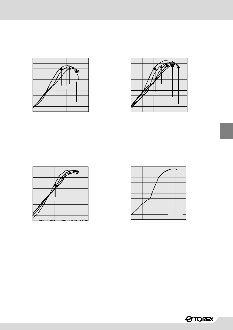
(2) EFFICIENCY vs. OUTPUT CURRENT
L=22
µH, C
L
=40
µF (Ceramic), C
IN
=30
µF (Ceramic)
R
SEN
=50m
, C
DD
=1
µF (Ceramic), SD:U3FWJ44N
C
GAIN
=470pF (Ceramic), Tr:XP162A11C0PR
L=22
µH, C
L
=40
µF (Ceramic), C
IN
=30
µF (Ceramic)
R
SEN
=50m
, C
DD
=1
µF (Ceramic), SD:U3FWJ44N
C
GAIN
=470pF (Ceramic), Tr:XP162A11C0PR
L=22
µH, C
L
=40
µF (Ceramic), C
IN
=30
µF (Ceramic)
R
SEN
=50m
, C
DD
=1
µF (Ceramic), SD:U3FWJ44N
C
GAIN
=470pF (Ceramic), Tr:XP162A11C0PR
L=68
µH, C
L
=40
µF (Ceramic), C
IN
=30
µF (Ceramic)
R
SEN
=50m
, C
DD
=10
µF (Ceramic), SD:U3FWJ44N
C
GAIN
=470pF (Ceramic), Tr:XP132A11C0PR
V
OUT
1.5V, F
OSC
: 330kHz
V
OUT
3.3V, F
OSC
: 330kHz
V
OUT
5.0V, F
OSC
: 330kHz
V
OUT
12.0V, F
OSC
: 100kHz
0
20
40
60
80
100
0.1
1
10
100
1000
10000
Output Current : I
OUT
(mA)
Efficiency : EFFI (%)
V
IN
=18.0V
0
20
40
60
80
100
0.1
1
10
100
1000
10000
Output Current : I
OUT
(mA)
Efficiency : EFFI (%)
V
IN
=8.0V
12.0V
10.0
15.0V
0
20
40
60
80
100
0.1
1
10
100
1000
10000
Output Current : I
OUT
(mA)
Efficiency : EFFI (%)
V
IN
=4.0V
10.0V
8.0V
6.0V
12.0V
0
20
40
60
80
100
0.1
1
10
100
1000
10000
Output Current : I
OUT
(mA)
Efficiency : EFFI (%)
V
IN
=3.3V
5.0V
7.2V
05S_1XC9201/9202 02.09.12 15:16 553

XC9201
Series
554
5
(3) RIPPLE VOLTAGE vs. OUTPUT CURRENT
L=22
µH, C
L
=40
µF (Ceramic), C
IN
=30
µF (Ceramic)
R
SEN
=50m
, C
DD
=1
µF (Ceramic), SD:U3FWJ44N
C
GAIN
=470pF (Ceramic), Tr:XP162A11C0PR
L=22
µH, C
L
=40
µF (Ceramic), C
IN
=30
µF (Ceramic)
R
SEN
=50m
, C
DD
=1
µF (Ceramic), CD:U3FWJ44N
C
GAIN
=470pF (Ceramic), Tr:XP162A11C0PR
L=22
µH, C
L
=40
µF (Ceramic), C
IN
=30
µF (Ceramic)
R
SEN
=50m
, C
DD
=1
µF (Ceramic), SD:U3FWJ44N
C
GAIN
=470pF (Ceramic), Tr:XP162A11C0PR
L=68
µH, C
L
=40
µF (Ceramic), C
IN
=30
µF (Ceramic)
R
SEN
=50m
, C
DD
=10
µF (Ceramic), SD:U3FWJ44N
C
GAIN
=470pF (Ceramic), Tr:XP132A11C0PR
V
OUT
1.5V, F
OSC
: 330kHz
V
OUT
3.3V, F
OSC
: 330kHz
V
OUT
5.0V, F
OSC
: 330kHz
V
OUT
12.0V, F
OSC
: 100kHz
L=22
µH, C
L
=47
µF (Tantalum), C
IN
=47
µF (Tantalum)
R
SEN
=50m
, C
DD
=1
µF (Ceramic), SD:U3FWJ44N
C
GAIN
=470pF (Ceramic), Tr:XP162A11C0PR
L=22
µH, C
L
=47
µF (Tantalum), C
IN
=47
µF (Tantalum)
R
SEN
=50m
, C
DD
=1
µF (Ceramic), SD:U3FWJ44N
C
GAIN
=470pF (Ceramic), Tr:XP162A11C0PR
V
OUT
1.5V, F
OSC
: 330kHz
V
OUT
3.3V, F
OSC
: 330kHz
0
20
40
60
80
100
0.1
1
10
100
1000
10000
Output Current : I
OUT
(mA)
0
20
40
60
80
100
0.1
1
10
100
1000
10000
Output Current : I
OUT
(mA)
0
20
40
60
80
100
0.1
1
10
100
1000
10000
Output Current : I
OUT
(mA)
0
20
40
60
80
100
0.1
1
10
100
1000
10000
Output Current : I
OUT
(mA)
0
20
40
60
80
100
0.1
1
10
100
1000
10000
Output Current : I
OUT
(mA)
0
20
40
60
80
100
0.1
1
10
100
1000
10000
Output Current : I
OUT
(mA)
Ripple Voltage : Vr (mVp-p)
Ripple Voltage : Vr (mVp-p)
Ripple Voltage : Vr (mVp-p)
Ripple Voltage : Vr (mVp-p)
Ripple Voltage : Vr (mVp-p)
Ripple Voltage : Vr (mVp-p)
V
IN
=4.0V
6.0V
8.0V
10.0V
12.0V
V
IN
=3.3V
5.0V
7.2V
V
IN
=18.0V
V
IN
=8.0V
15.0V
10.0V
12.0V
6.0V
8.0V 10.0V
12.0V
V
IN
=4.0V
V
IN
=3.3V
7.2V
5.0V
*Note: If the input and output voltage differential is large or small, the time of ON and Off switching will be shorten.
This gives external components such as inductance value of coil, connecting a resistor to CLK, condenser, will critically influence the
actual operation.
05S_1XC9201/9202 02.09.12 15:16 554