PWM, PWM/PFM Switching Step-Up & Down DC/DC Converter Controller ICs
Series
597
6
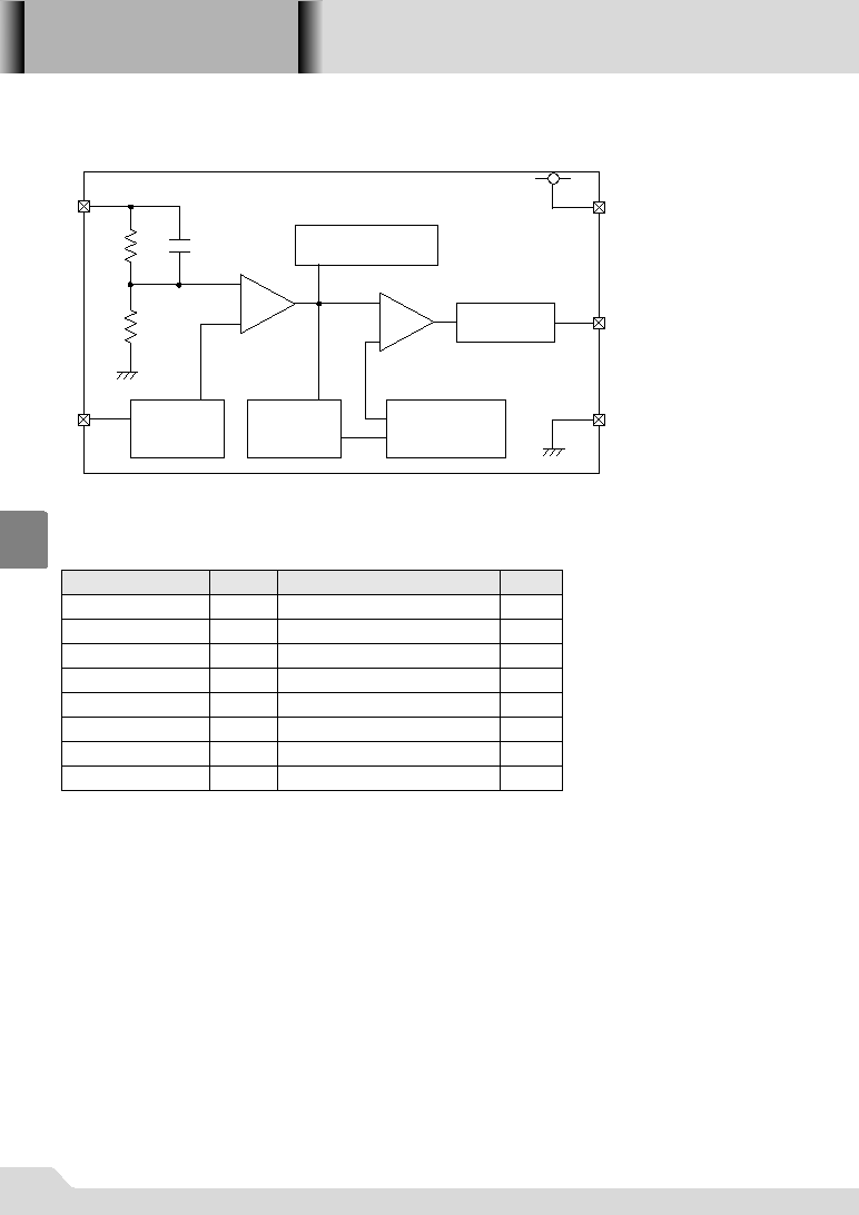
The XC9301/02 series are step-up/down DC/DC converter controller ICs
with fast, low ON resistance drivers built-in. A versatile, large output
current, step-up/down DC/DC converter can be realised using only 4
basic external components - transistors, coils, diodes and capacitors.
Output voltage is selectable in 0.1V steps within a 2.4V ~ 6.0V ( ± 2.5%
accuracy) range and switching frequency is set at 180kHz or 300KHz.
The XC9302 series switches from PWM to PFM control during light loads
and the series offers high efficiencies from light loads through to large
output currents.
Soft-start time is internally set to 10 msec which offers protection against
rush currents when the power is switched on and also against voltage
overshoot.
During shutdown (CE pin = L), consumption current can be reduced to
as little as 0.5
µA or less.
Input Voltage Range
: 2.0V ~ 10V
Output Voltage Range : 2.4V ~ 6.0V ( ± 2.5% accuracy)
(selectable in 0.1V steps)
Oscillation Frequency : 180KHz, 300KHz ( ± 15% accuracy)
Output Current
: more than 250mA (V
IN
=2.4V,
V
OUT
=3.3V)
Efficiency
: 81% (typ) at 5.0V, 78% (typ) at 3.3V
Stand-By
: ISTB = 0.5
µA (max)
Output Voltage Internal Set-Up
SOT-25 Package
GMobile phones
GPDAs
GPalmtop computers
GPortable audio equipment
GVarious power supplies
Features
Applications
NInput Voltage Range : 2.0V ~10.0V
NOutput Voltage Range : 2.4V ~ 6.0V (±2.5% accuracy)
NOscillation Frequency Range
: 180kHz, 300kHz (±15% accuracy)
NMaximum Duty Ratio : 85% (typ)
NPWM/PFM Switching Step-Up & Down Control (XC9302)
NEfficiency
: 81% (typ) 5.0V , 78% (typ) 3.3V
NSOT-25 Package
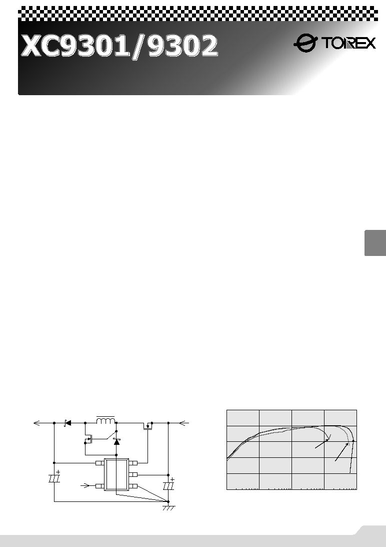
CE
C
L
SD1
V
OUT
V
IN
C
IN
SD2
PSW
NSW
L
Typical Application Circuit
Typical Performance Characteristic
0
20
40
60
80
100
0. 1
1
10
100
1000
V
IN
=2V
6V
4V
Efficiency:EFFI %
Output Current:I
OUT
mA
General Description
06S_15XC9301/02 02.9.12 3:28 PM 597
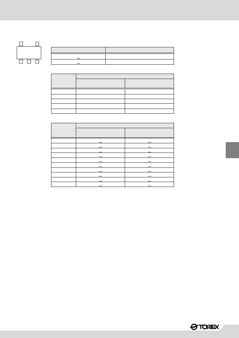
Marking
SOT-25
(TOP VIEW)
q w e r
DESIGNATOR
PRODUCT NAME
XC9302AM
XC9301AM
q Represents the Product Classification
w Represents the integer of the Output Voltage and Oscillation Frequency
FREQUENCY=180
kHz
XC9301/XC9302A2M
DESIGNATOR
OUTPUT
VOLTAGEV
5.X
4.X
3.X
2.X
r Denotes the production lot number
0 to 9, A to Z repeated(G.I.J.O.Q.W excepted)
6.X
FREQUENCY=300
kHz
XC9301/XC9302A3M
2
3
4
5
6
2
3
4
5
6
e Represents the decimal number of the Output Voltage and Oscillation Frequency
X.0
X.9
FREQUENCY=180
kHz
XC9301/XC9302A2M
DESIGNATOR
OUTPUT
VOLTAGEV
X.8
X.7
X.6
X.1
X.5
X.4
X.3
X.2
FREQUENCY=300
kHz
XC9301/XC9302A3M
A
B
C
D
E
H
K
L
M
F
0
1
2
3
4
6
7
8
9
5
A
K
XC9301/9302
Series
599
6
06S_15XC9301/02 02.9.12 3:28 PM 599

XC9301/9302
Series
601
6
Typical Application Circuit
GCircuit Connection Example
Electrical Characteristics
XC9301x332MR,XC9302x332MR
Measuring Conditions : Unless otherwise stated, V
DD
= 3.3V, I
OUT
= 130mA
Note: 1. XC9302 series only
2. EFFI={[(Output Voltage) × (Output Current)] ÷ [(Input Voltage) × (Input Current)]} × 100
PARAMETER
SYMBOL
CONDITIONS
Output Voltage
Supply Voltage
Supply Current 1
V
OUT
=CE: Set Output Voltage × 0.95 applied
Supply Current 2
V
OUT
=CE: Set Output Voltage + 0.5 applied
Stand-By Current
V
OUT
: Set Output Voltage × 0.95 applied, CE=0V
Oscillation Frequency
V
DD
=V
OUT
=CE: Set Output Voltage × 0.95 applied
Max. Duty Ratio
V
DD
=V
OUT
=CE: Set Output Voltage × 0.95 applied
PFM Duty Ratio
Note1
No Load
Efficiency
Note2
V
DD
=V
IN
=CE: Set Output Voltage × 0.95 applied
Soft-Start Time
CE 'H' Voltage
V
OUT
: Set Output Voltage × 0.95 applied
CE 'L' Voltage
V
OUT
: Set Output Voltage × 0.95 applied
EXT/ 'H' ON Resistance
Same as I
DD
1, V
EXT
/ = V
OUT
- 0.4V
EXT/ 'L' ON Resistance
Same as I
DD
1, V
EXT
/ = 0.4V
UNITS
V
V
A
A
A
KHz
%
%
%
mS
V
V
MAX.
3.383
10.0
140
26
0.5
207
92
35
20.0
0.20
43
27
TYP.
80
15
180
85
25
78
10.0
29
19
MIN.
3.218
3.300
2.0
153
78
15
5.0
0.65
(V
OUT
=3.3V, F
OSC
=180kHz)
Ta=25
V
OUT
V
DD
I
DD
1
I
DD
2
I
STB
F
OSC
MAXDTY
PFMDTY
EFFI
T
SS
V
CEH
V
CEL
R
EXTBH
R
EXTBL
XC9301x333MR, XC9302x333MR
PARAMETER
SYMBOL
CONDITIONS
Output Voltage
V
OUT
Supply Voltage
V
DD
Supply Current 1
I
DD
1
V
OUT
=CE: Set Output Voltage × 0.95 applied
Supply Current 2
I
DD
2
V
OUT
=CE: Set Output Voltage + 0.5 applied
Stand-By Current
I
STB
V
OUT
: Set Output Voltage x 0.95 applied, CE=0V
Oscillation Frequency
F
OSC
V
DD
=V
OUT
=CE: Set Output Voltage × 0.95 applied
Max. Duty Ratio
MAXDTY V
DD
=V
OUT
=CE: Set Output Voltage × 0.95 applied
PFM Duty Ratio
Note1
PFMDTY No Load
Efficiency
Note2
EFFI
V
DD
=V
IN
=CE: Set Output Voltage × 0.95 applied
Soft-Start Time
T
SS
CE 'H' Voltage
V
CEH
V
OUT
: Set Output Voltage × 0.95 applied
CE 'L' Voltage
V
CEL
V
OUT
: Set Output Voltage × 0.95 applied
EXT/ 'H' ON Resistance R
EXTBH
Same as I
DD
1, V
EXT
/ = V
OUT
- 0.4V
EXT/ 'L' ON Resistance R
EXTBL
Same as I
DD
1, V
EXT
/ = 0.4V
V
V
A
A
A
KHz
%
%
%
mS
V
V
MAX.
3.383
10.0
200
35
0.5
345
92
35
20.0
0.20
43
27
TYP.
130
20
300
85
25
78
10.0
29
19
MIN.
3.218
3.300
2.0
255
78
15
5.0
0.65
Measuring Conditions : Unless otherwise stated, V
DD
= 3.3V, I
OUT
= 130mA
Note: 1. XC9302 series only
2. EFFI={[(Output Voltage) × (Output Current)] ÷ [(Input Voltage) × (Input Current)]} × 100
(V
OUT
=3.3V, F
OSC
=300kHz)
Ta=25
UNITS
External Components
PSW : XP162A12 ( SOT-89 pkg, Torex )
NSW : XP161A12 ( SOT-89 pkg, Torex )
L
: 22H ( Sumida CR54 )
SD : U2FWJ44N ( Schottky, Toshiba )
C
L
: 16V, 47F × 2 ( Tantalum, Nichicon MCE )
C
IN
: 16V, 22F ( Tantalum, Nichicon MCE )
220F (Nichicon, PJ)
CE
C
L
SD1
V
OUT
V
IN
C
IN
SD2
PSW
NSW
L
06S_15XC9301/02 02.9.12 3:28 PM 601