2SC5859
2004-5-18
1
TOSHIBA TRANSISTOR SILICON NPN TRIPLE DIFFUSED MESA TYPE
2SC5859
HORIZONTAL DEFLECTION OUTPUT FOR
HDTV, DIGITAL TV, PROJECTION TV
High Voltage
: V
CBO
= 1700 V
Low Saturation Voltage : V
CE
(sat)
= 3 V (max)
High Speed
: t
f(2)
= 0.1 µs (Typ.)
MAXIMUM RATINGS
(Tc = 25∞C)
CHARACTERISTIC SYMBOL
RATING
UNIT
Collector-Base Voltage
V
CBO
1700 V
Collector-Emitter Voltage
V
CEO
750 V
Emitter-Base Voltage
V
EBO
5 V
DC I
C
23
Collector Current
Pulse
I
CP
46
A
Base Current
I
B
11.5 A
Collector Power Dissipation
P
C
210 W
Junction Temperature
T
j
150 ∞C
Storage Temperature Range
T
stg
-55~150 ∞C
ELECTRICAL CHARACTERISTICS
(Tc = 25∞C)
CHARACTERISTIC SYMBOL TEST
CONDITION Min
Typ.
Max
UNIT
Collector Cut-off Current
I
CBO
V
CB
= 1700 V, I
E
= 0
1 mA
Emitter Cut-off Current
I
EBO
V
EB
= 5 V, I
C
= 0
100 µA
Collector - Emitter Breakdown Voltage V
(BR)
CEO
I
C
= 10 mA, I
B
= 0
750
V
h
FE
(1)
V
CE
= 5 V, I
C
= 2 A
20
55
h
FE
(2)
V
CE
= 5 V, I
C
= 8 A
10
22
DC Current Gain
h
FE
(3)
V
CE
= 5 V, I
C
= 18 A
4.5
8
Collector-Emitter Saturation Voltage
V
CE
(sat)
I
C
= 18 A, I
B
= 4.5 A
3 V
Base-Emitter Saturation Voltage
V
BE
(sat)
I
C
= 18 A, I
B
= 4.5 A
1.0 1.5 V
Transition Frequency
f
T
V
CE
= 10 V, I
C
= 0.1 A
2 MHz
Collector Output Capacitance
C
ob
V
CB
= 10 V, I
E
= 0, f = 1 MHz
320 pF
Storage Time
t
stg(1)
4
Fall Time
t
f(1)
I
CP
= 8 A , I
B1
(end) = 1 A
f
H
= 32 kHz
0.15
µs
Storage Time
t
stg(2)
1.8
Switching Time
Fall Time
t
f(2)
I
CP
= 7.5 A, I
B1
(end) = 1 A
f
H
= 100 kHz
0.1
µs
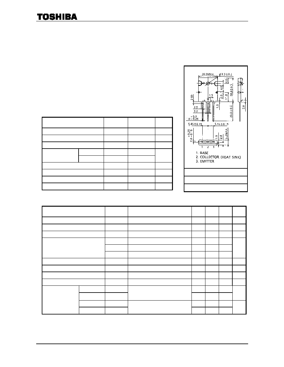
Unit: mm
JEDEC
JEITA
TOSHIBA 2-21F2A
Weight: 9.75 g (typ.)
2SC5859
2004-5-18
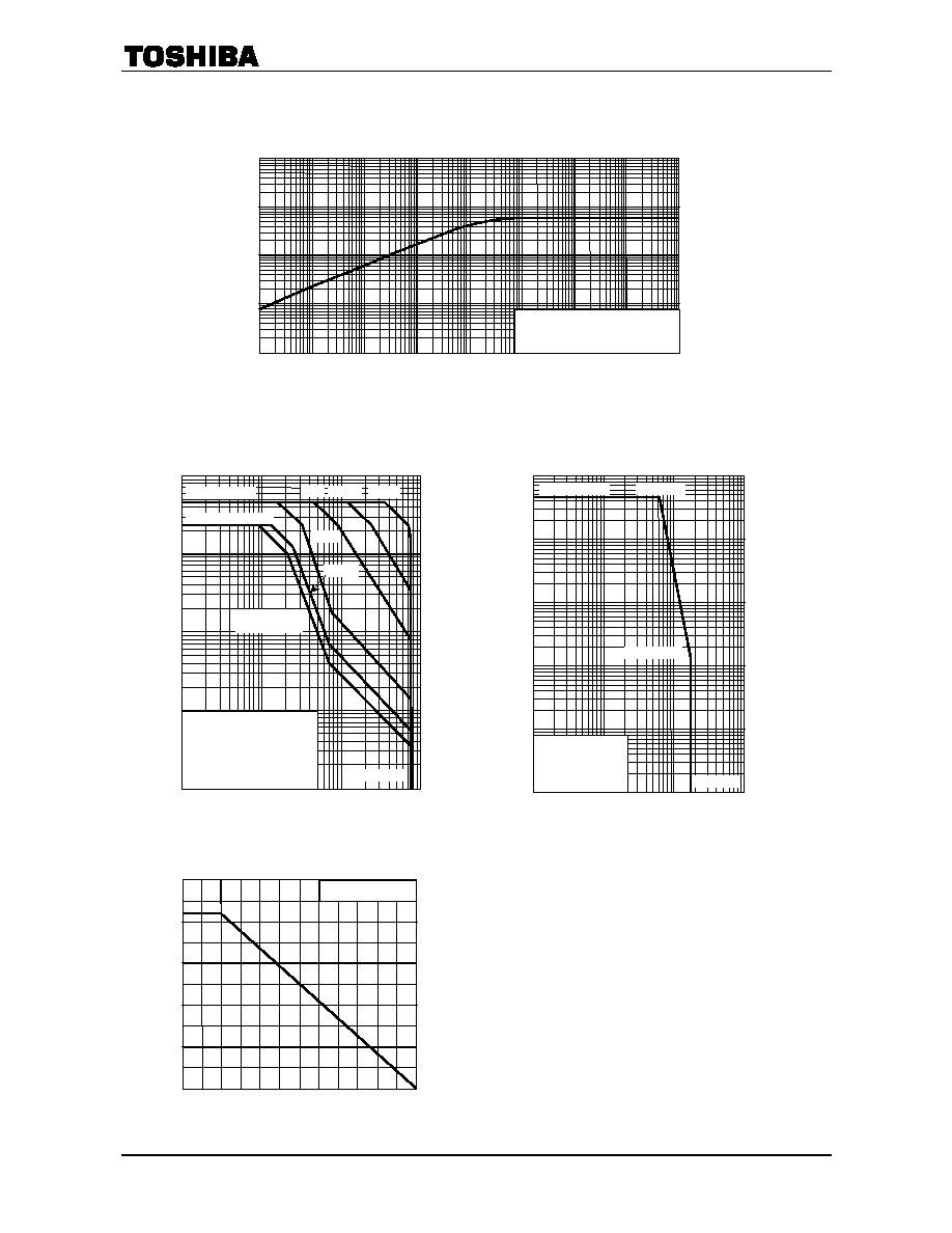
4
P
C
≠ Tc
r
th(j-c)
≠ t
w
T
r
a
n
s
i
e
n
t t
h
e
r
m
a
l im
pe
da
nce
(ju
n
c
t
ion
-
ca
se
)
r th
(
j
-
c
)
(∞
C
/
W
)
Pulse width tw (s)
10
0.001
10
1000
100 1m
100m
10 100
0.01
1
Tc = 25 (Infinite heat sink)
Curves should be applied in thermal
limited area. (single nonrepetitive pulse)
0.1
10m
1
Collector-emitter voltage V
CE
(V)
Safe Operating Area
C
o
llec
t
or
cur
r
e
n
t I
C
(
A
)
0.01
100
1 ms*
10 ms*
VCEO max
100 µs*
100 ms*
IC max (Continuous)*
1
100 1000
10
1
10
0.1
10 µs*
DC operation
Tc = 25∞C
*: Single nonrepetitive pulse
Tc = 25∞C
Curves must be derated
linearly with increase in
temperature.
IC max (Pulse)*
Col
l
ect
o
r po
w
e
r dissi
p
a
ti
on
P
C
(W
)
Case temperature Tc (∞C)
0
0
25
75
100
125
150
50
150
200
250
100
50
Infinite heat sink
Collector-emitter voltage V
CE
(V)
Reverse Bias ≠ Safe Operating Area
C
o
llect
or c
u
rre
n
t
I C
(
A
)
100
0.1
0.001
10
10000
10 100
Ta = 25
Non repeated pulse
IB2 = -3A
L = 500 H
1
0.01
1000
VCBO max
IC max (Pulse)
620V,46A
1700V,0.14A
2SC5859
2004-5-18
5
∑ The information contained herein is subject to change without notice.
∑ The information contained herein is presented only as a guide for the applications of our products. No
responsibility is assumed by TOSHIBA for any infringements of patents or other rights of the third parties which
may result from its use. No license is granted by implication or otherwise under any patent or patent rights of
TOSHIBA or others.
∑ TOSHIBA is continually working to improve the quality and reliability of its products. Nevertheless, semiconductor
devices in general can malfunction or fail due to their inherent electrical sensitivity and vulnerability to physical
stress. It is the responsibility of the buyer, when utilizing TOSHIBA products, to comply with the standards of
safety in making a safe design for the entire system, and to avoid situations in which a malfunction or failure of
such TOSHIBA products could cause loss of human life, bodily injury or damage to property.
In developing your designs, please ensure that TOSHIBA products are used within specified operating ranges as
set forth in the most recent TOSHIBA products specifications. Also, please keep in mind the precautions and
conditions set forth in the "Handling Guide for Semiconductor Devices," or "TOSHIBA Semiconductor Reliability
Handbook" etc..
∑ The TOSHIBA products listed in this document are intended for usage in general electronics applications
(computer, personal equipment, office equipment, measuring equipment, industrial robotics, domestic appliances,
etc.). These TOSHIBA products are neither intended nor warranted for usage in equipment that requires
extraordinarily high quality and/or reliability or a malfunction or failure of which may cause loss of human life or
bodily injury ("Unintended Usage"). Unintended Usage include atomic energy control instruments, airplane or
spaceship instruments, transportation instruments, traffic signal instruments, combustion control instruments,
medical instruments, all types of safety devices, etc.. Unintended Usage of TOSHIBA products listed in this
document shall be made at the customer's own risk.
∑ TOSHIBA products should not be embedded to the downstream products which are prohibited to be produced
and sold, under any law and regulations.
030619EAA
RESTRICTIONS ON PRODUCT USE