2SK3569
2004-03-04
1
TOSHIBA Field Effect Transistor Silicon N Channel MOS Type (-MOSVI)
2SK3569
Switching Regulator Applications
∑
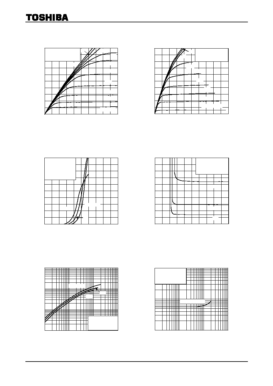
Low drain-source ON resistance: R
DS (ON)
= 0.54 (typ.)
∑
High forward transfer admittance: |Y
fs
| = 8.5S (typ.)
∑
Low leakage current: I
DSS
= 100 A (V
DS
= 600 V)
∑
Enhancement-mode: V
th
= 2.0~4.0 V (V
DS
= 10 V, I
D
= 1 mA)
Maximum Ratings
(Ta
=
=
=
=
25∞C)
Characteristics Symbol
Rating
Unit
Drain-source voltage
V
DSS
600 V
Drain-gate voltage (R
GS
=
20 k
) V
DGR
600 V
Gate-source voltage
V
GSS
±
30 V
DC (Note
1)
I
D
10
Drain current
Pulse (t
=
1 ms)
(Note
1)
I
DP
40
A
Drain power dissipation (Tc
=
25∞C)
P
D
45 W
Single pulse avalanche energy
(Note
2)
E
AS
363 mJ
Avalanche current
I
AR
10 A
Repetitive avalanche energy (Note 3)
E
AR
4.5
mJ
Channel temperature
T
ch
150
∞C
Storage temperature range
T
stg
-55~150 ∞C
Thermal Characteristics
Characteristics Symbol
Max
Unit
Thermal resistance, channel to case
R
th (ch-c)
2.78
∞C/W
Thermal resistance, channel to ambient
R
th (ch-a)
62.5
∞C/W
Note 1: Please use devices on conditions that the channel temperature is below 150∞C.
Note 2: V
DD
=
90 V, T
ch
=
25∞C(initial), L
=
6.36 mH, I
AR
=
10 A, R
G
=
25
Note 3: Repetitive rating: Pulse width limited by maximum channel temperature
This transistor is an electrostatic sensitive device. Please handle with caution.
Unit: mm
1: Gate
2: Drain
3: Source
JEDEC
JEITA SC-67
TOSHIBA 2-10U1B
Weight : 1.7 g (typ.)
1
3
2

2SK3569
2004-03-04
2
Electrical Characteristics
(Ta
=
=
=
=
25∞C)
Characteristics Symbol Test
Condition Min
Typ.
Max
Unit
Gate leakage current
I
GSS
V
GS
=
±
25 V, V
DS
=
0 V
±
10
µ
A
Gate-source breakdown voltage
V
(BR) GSS
I
G
=
±
10
µ
A, V
DS
=
0 V
±
30
V
Drain cut-off current
I
DSS
V
DS
=
600 V, V
GS
=
0 V
100
µ
A
Drain-source breakdown voltage
V
(BR) DSS
I
D
=
10 mA, V
GS
=
0 V
600
V
Gate threshold voltage
V
th
V
DS
=
10 V, I
D
=
1 mA
2.0
4.0 V
Drain-source ON resistance
R
DS (ON)
V
GS
=
10 V, I
D
=
5 A
0.54 0.75
Forward transfer admittance
Y
fs
V
DS
=
10 V, I
D
=
5 A
0.7
8.5
S
Input capacitance
C
iss
1500
Reverse transfer capacitance
C
rss
15
Output capacitance
C
oss
V
DS
=
25 V, V
GS
=
0 V, f
=
1 MHz
180
pF
Rise time
t
r
22
Turn-on time
t
on
50
Fall time
t
f
36
Switching time
Turn-off time
t
off
180
ns
Total gate charge
Q
g
42
Gate-source charge
Q
gs
23
Gate-drain charge
Q
gd
V
DD
-
400 V, V
GS
=
10 V, I
D
=
10 A
19
nC
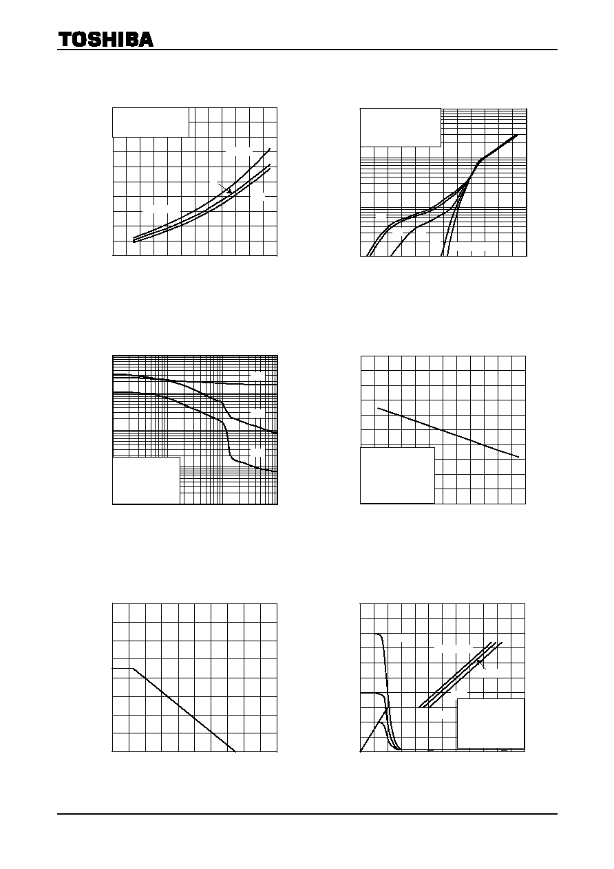
Source-Drain Ratings and Characteristics
(Ta
=
=
=
=
25∞C)
Characteristics Symbol
Test
Condition
Min
Typ.
Max
Unit
Continuous drain reverse current
(Note
1)
I
DR
10 A
Pulse drain reverse current
(Note 1)
I
DRP
40 A
Forward voltage (diode)
V
DSF
I
DR
=
10 A, V
GS
=
0 V
-
1.7
V
Reverse recovery time
t
rr
1300
ns
Reverse recovery charge
Q
rr
I
DR
=
10 A, V
GS
=
0 V,
dI
DR
/dt
=
100 A/
µ
s
16
µ
C
Marking
R
L
=
40
0 V
10
V
V
GS
V
DD
-
200 V
I
D
=
5
A V
OUT
50
Duty
<
=
1%, t
w
=
10
µ
s
Lot Number
TYPE
K3569

2SK3569
2004-03-04
5
500
400
300
200
100
0
25 50 75 100 125
150
0.01
10
0.1
1
10
100
1
10
100
1
10
T
PDM
t
Duty
=
t/T
Rth (ch-c)
=
2.78∞C/W
Duty=0.5
0.2
0.1
0.05
0.02
0.01
0.001
0.1
1
1
10
100
10
1000
100
VDSS max
0.01
CHANNEL TEMPERATURE (INITIAL)
T
ch
(∞C)
E
AS
≠ T
ch
A
V
A
LA
NCHE
E
N
E
R
GY
E
AS
(
m
J
)
r
th
≠ t
w
PULSE WIDTH t
w
(s)
N
O
R
M
AL
IZED
TR
AN
SIEN
T TH
ER
M
A
L
I
M
P
E
DA
NCE
r
th (t)
/R
th (ch-c)
Duty=0.5
SINGLE PULSE
-
15
V
15
V
TEST CIRCUIT
WAVE FORM
I
AR
B
VDSS
V
DD
V
DS
R
G
=
25
V
DD
=
90 V, L
=
6.36mH
-
=
VDD
BVDSS
BVDSS
2
I
L
2
1
AS
DRAIN-SOURCE VOLTAGE V
DS
(V)
SAFE OPERATING AREA
SINGLE NONREPETITIVE PULSE
Tc=25
CURVES MUST BE DERATED
LINEARLY WITH INCREASE IN
TEMPERATURE.
ID max (PULSED) *
ID max (CONTINUOUS) *
DC OPERATION
Tc
=
25∞C
100
µ
s *
1 ms *
DRA
I
N
CURRE
N
T
I
D
(A
)