30QWK2C48
2000-11-20 1/4
TOSHIBA Schottky Barrier Rectifier Stack Trench Schottky Barrier Type
3 0 Q W K 2 C 4 8
Switching Type Power Supply Application
Converter & Chopper Application
∑ Repetitive peak reverse voltage: V
RRM
= 120 V
∑ Peak Forward Voltage: V
FM
= 0.85 V (max)
∑ Average output rectified current: I
O
= 30 A
∑ Low switching loses and output noise.
Maximum Ratings
Characteristics Symbol
Rating
Unit
Repetitive peak reverse voltage
V
RRM
120 V
Average output rectified current
I
O
30
A
Peak one cycle surge forward current
(sine wave)
I
FSM
250 (50 Hz)
A
Junction temperature
T
j
-40~150 ∞C
Storage temperature range
T
stg
-40~150 ∞C
Electrical Characteristics
(Ta
=
=
=
= 25∞C)
Characteristics Symbol
Test
Condition
Min
Typ.
Max
Unit
Peak forward voltage
V
FM
I
FM
= 15 A
0.85 V
Repetitive peak reverse current
I
RRM
V
RRM
= Rated (120 V)
50 µA
Junction capacitance
C
j
V
R
= 10 V, f = 1.0 MHz
227 pF
Thermal resistance
R
th (j-c)
DC
Total
1.2
∞C/W
Note: V
FM
, I
RRM
, C
j
: A value of one cell.
∑ TOSHIBA is continually working to improve the quality and reliability of its products. Nevertheless, semiconductor devices in general
can malfunction or fail due to their inherent electrical sensitivity and vulnerability to physical stress. It is the responsibility of the
buyer, when utilizing TOSHIBA products, to comply with the standards of safety in making a safe design for the entire system, and
to avoid situations in which a malfunction or failure of such TOSHIBA products could cause loss of human life, bodily injury or
damage to property.
In developing your designs, please ensure that TOSHIBA products are used within specified operating ranges as set forth in the
most recent TOSHIBA products specifications. Also, please keep in mind the precautions and conditions set forth in the "Handling
Guide for Semiconductor Devices," or "TOSHIBA Semiconductor Reliability Handbook" etc..
∑ The TOSHIBA products listed in this document are intended for usage in general electronics applications (computer, personal
equipment, office equipment, measuring equipment, industrial robotics, domestic appliances, etc.). These TOSHIBA products are
neither intended nor warranted for usage in equipment that requires extraordinarily high quality and/or reliability or a malfunction or
failure of which may cause loss of human life or bodily injury ("Unintended Usage"). Unintended Usage include atomic energy
control instruments, airplane or spaceship instruments, transportation instruments, traffic signal instruments, combustion control
instruments, medical instruments, all types of safety devices, etc.. Unintended Usage of TOSHIBA products listed in this document
shall be made at the customer's own risk.
∑ The information contained herein is presented only as a guide for the applications of our products. No responsibility is assumed by
TOSHIBA CORPORATION for any infringements of intellectual property or other rights of the third parties which may result from its
use. No license is granted by implication or otherwise under any intellectual property or other rights of TOSHIBA CORPORATION or
others.
∑ The information contained herein is subject to change without notice.
000707EAA1
30QWK2C48
2000-11-20 2/4
Polarity Marking
Handling Precaution
Schottky barrier diodes are having large-reverse-current-leakage characteristic compare to other rectifier
products. This current leakage and not proper operating temperature or voltage may cause thermal run.
Please take forward and reverse loss into consideration when you design.
2
1
1 MARK
30QWK2C
TYPE
30QWK2C48
2
Lot Number
Month (starting from alphabet A)
Year (last number of the christian era)
30QWK2C48
2000-11-20 3/4
T
r
ansi
e
nt t
h
e
r
m
a
l
i
m
pe
da
nce
r th (j
-c
) (
∞
C
/
W
)
S
u
rg
e f
o
r
w
a
r
d
c
u
rre
nt
I
FSM
(A
)
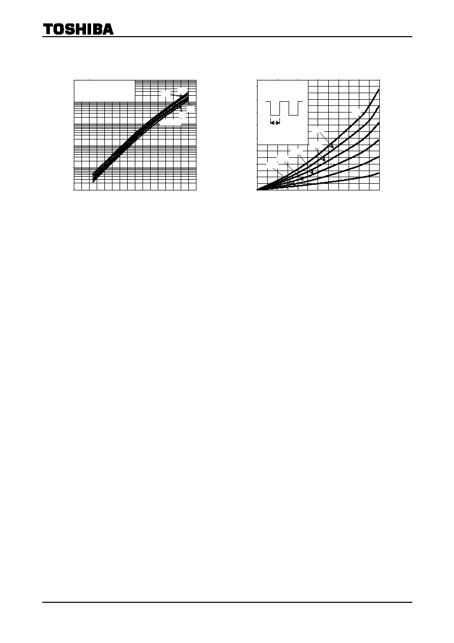
Instantaneous forward voltage vF (V)
i
F
≠ v
F
Insta
n
t
ane
ous
fo
r
w
a
r
d
cur
r
e
n
t i
F
(A
)
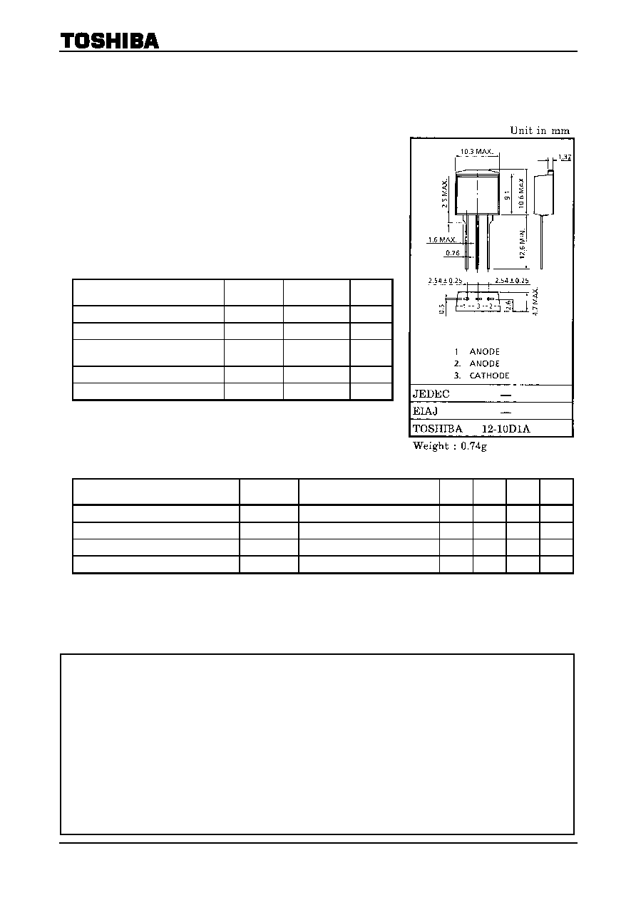
Average output rectified current I
o
(A)
P
F (AV)
≠ I
o
A
v
era
ge for
w
ar
d po
w
e
r di
ssi
p
a
ti
o
n
P
F (A
V)
(
W
)
Average output rectified current Io (A)
Tc max ≠ I
o
A
v
era
ge for
w
ar
d po
w
e
r di
ssi
p
a
ti
o
n
Tc
m
a
x
(
∞
C
)
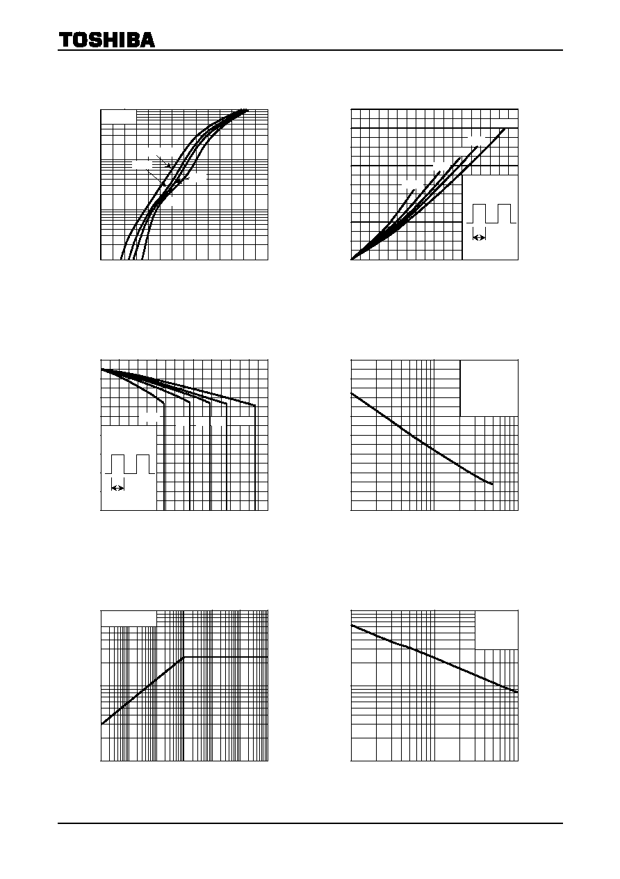
Number of cycles
Surge forward current (non-repetitive)
Time t (s)
r
th (j-c)
≠ t
Reverse voltage V
R
(V)
C
j
≠ V
R
(typical)
Juncti
on
cap
a
ci
t
anc
e C
j
(p
F)
0
0
160
36
180∞
120∞
= 30∞
60∞
90∞
140
120
100
80
60
40
20
32
28
24
20
16
4 8
12
360∞
0∞
Conduction
angle
Rectangular
waveform
(one cell)
0.1
0
100
Tj
= 150∞C
25∞C
75∞C
100∞C
One cell
1
10
0.2 0.4 0.6 0.8 1.0 1.2 1.4
32
0
0 36
180∞
120∞
= 30∞
60∞
90∞
28
24
20
16
12
8
4
4 8 12 16 20 24 28 32
360∞
0∞
Conduction
angle
Rectangular
waveform
(one cell)
320
1 100
Ta
= 25∞C
Single phase full
Sine wave
f
= 50 Hz
One cell
280
240
200
160
120
80
40
0
10
3 5
30
50
0.1
0.001
10
1000
1
0.01 0.1 1
100
10
One cell
0.3
3
5
0.5
1000
10
1 100
100
10
f
= 1 MHz
Ta
= 25∞C
One cell
5
3 30
50
30
300
500
50