 | –≠–ª–µ–∫—Ç—Ä–æ–Ω–Ω—ã–π –∫–æ–º–ø–æ–Ω–µ–Ω—Ç: GT40T301 | –°–∫–∞—á–∞—Ç—å:  PDF PDF  ZIP ZIP |
GT40T301
2002-01-18
1
TOSHIBA Insulated Gate Bipolar Transistor Silicon N Channel IGBT
GT40T301
Parallel Resonance Inverter Switching Applications
∑
FRD included between emitter and collector
∑
Enhancement-mode
∑
High speed IGBT : t
f
=
0.25 µs (typ.) (I
C
= 40 A)
FRD
:
t
rr
=
0.7 µs (typ.) (di/dt = -20 A/µs)
∑
Low saturation voltage: V
CE (sat)
= 3.7 V (typ.) (I
C
= 40 A)
Maximum Ratings
(Ta
=
=
=
=
25∞C)
Characteristics Symbol
Rating
Unit
Collector-emitter voltage
V
CES
1500 V
Gate-emitter voltage
V
GES
±
25 V
DC I
C
40
Collector current
1 ms
I
CP
80
A
DC I
ECF
30
Emitter-collector forward
current
1 ms
I
ECPF
80
A
Collector power dissipation (Tc
=
25∞C)
P
C
200
W
Junction temperature
T
j
150 ∞C
Storage temperature range
T
stg
-
55~150 ∞C
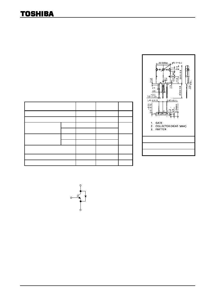
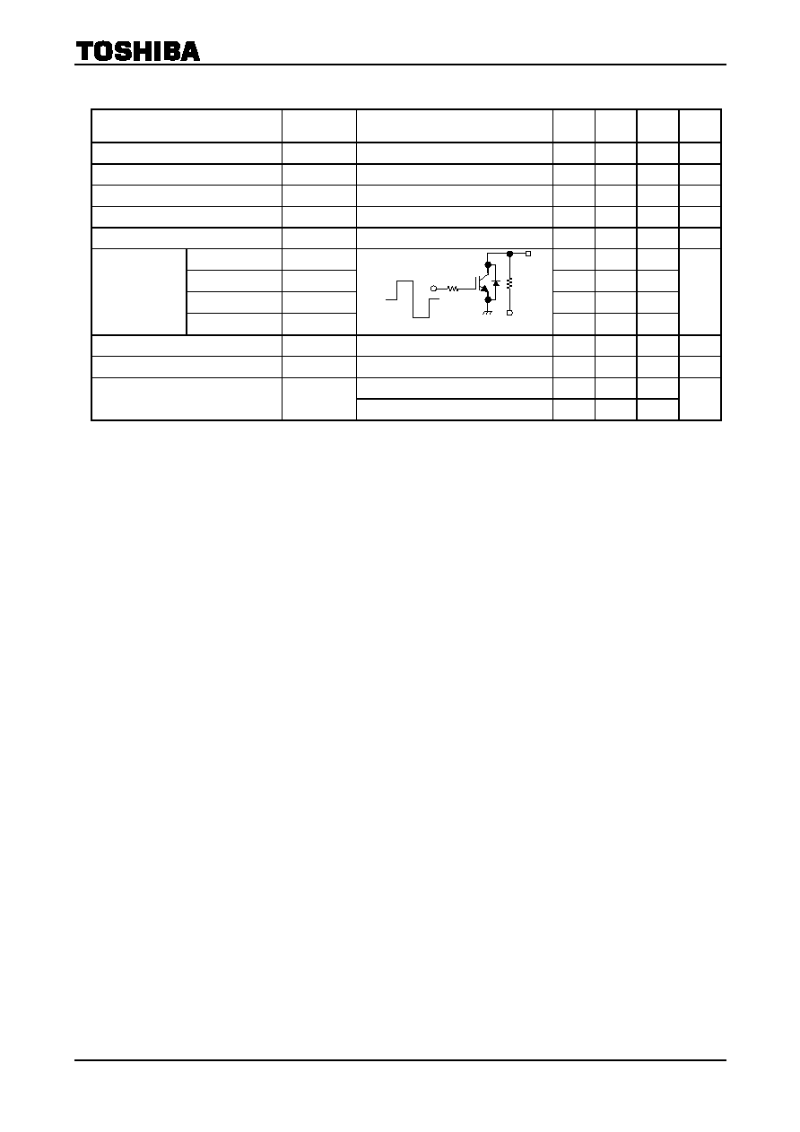
Equivalent Circuit
Unit: mm
JEDEC
JEITA
TOSHIBA 2-21F2C
Weight: 9.75 g (typ.)
Collector
Gate
Emitter
GT40T301
2002-01-18
2
Electrical Characteristics
(Ta
=
=
=
=
25∞C)
Characteristics Symbol Test
Condition Min
Typ.
Max
Unit
Gate leakage current
I
GES
V
GE
=
±
25 V, V
CE
=
0
±
500 nA
Collector cut-off current
I
CES
V
CE
=
1500 V, V
GE
=
0
1.0 mA
Gate-emitter cut-off voltage
V
GE (OFF)
I
C
=
40 mA, V
CE
=
5 V
4.0
7.0 V
Collector-emitter saturation voltage
V
CE (sat)
I
C
=
40 A, V
GE
=
15 V
3.7 5.0 V
Input capacitance
C
ies
V
CE
=
10 V, V
GE
=
0, f
=
1 MHz
2900
pF
Rise time
t
r
0.40
Turn-on time
t
on
0.45
Fall time
t
f
0.23 0.40
Switching time
Turn-off time
t
off
0.6
µ
s
Emitter-collector forward voltage
V
ECF
I
ECF
=
30 A, V
GE
=
0
1.9
2.5 V
Reverse recovery time
t
rr
I
ECF
=
30 A, V
GE
=
0, di/dt
=
-
20 A/
µ
s
0.7
3.0
µ
s
IGBT
0.625
Thermal resistance
R
th (j-c)
Diode
1.25
∞C/W
-
15 V
15 V
0
600 V
15
51

GT40T301
2002-01-18
3
Co
lle
ct
o
r
cu
r
r
e
n
t
I
C
(A
)
Co
lle
ct
o
r
-
e
m
i
tte
r
v
o
lta
g
e
V
CE
(V
)
Collector-emitter voltage V
CE
(V)
I
C
≠ V
CE
Co
lle
ct
o
r
cu
r
r
e
n
t
I
C
(A
)
Gate-emitter voltage V
GE
(V)
V
CE
≠ V
GE
Co
lle
ct
o
r
-
e
m
i
tte
r
v
o
lta
g
e
V
CE
(V
)
Gate-emitter voltage V
GE
(V)
V
CE
≠ V
GE
Co
lle
ct
o
r
-
e
m
i
tte
r
v
o
lta
g
e
V
CE
(V
)
Gate-emitter voltage V
GE
(V)
V
CE
≠ V
GE
Gate-emitter voltage V
GE
(V)
I
C
≠ V
GE
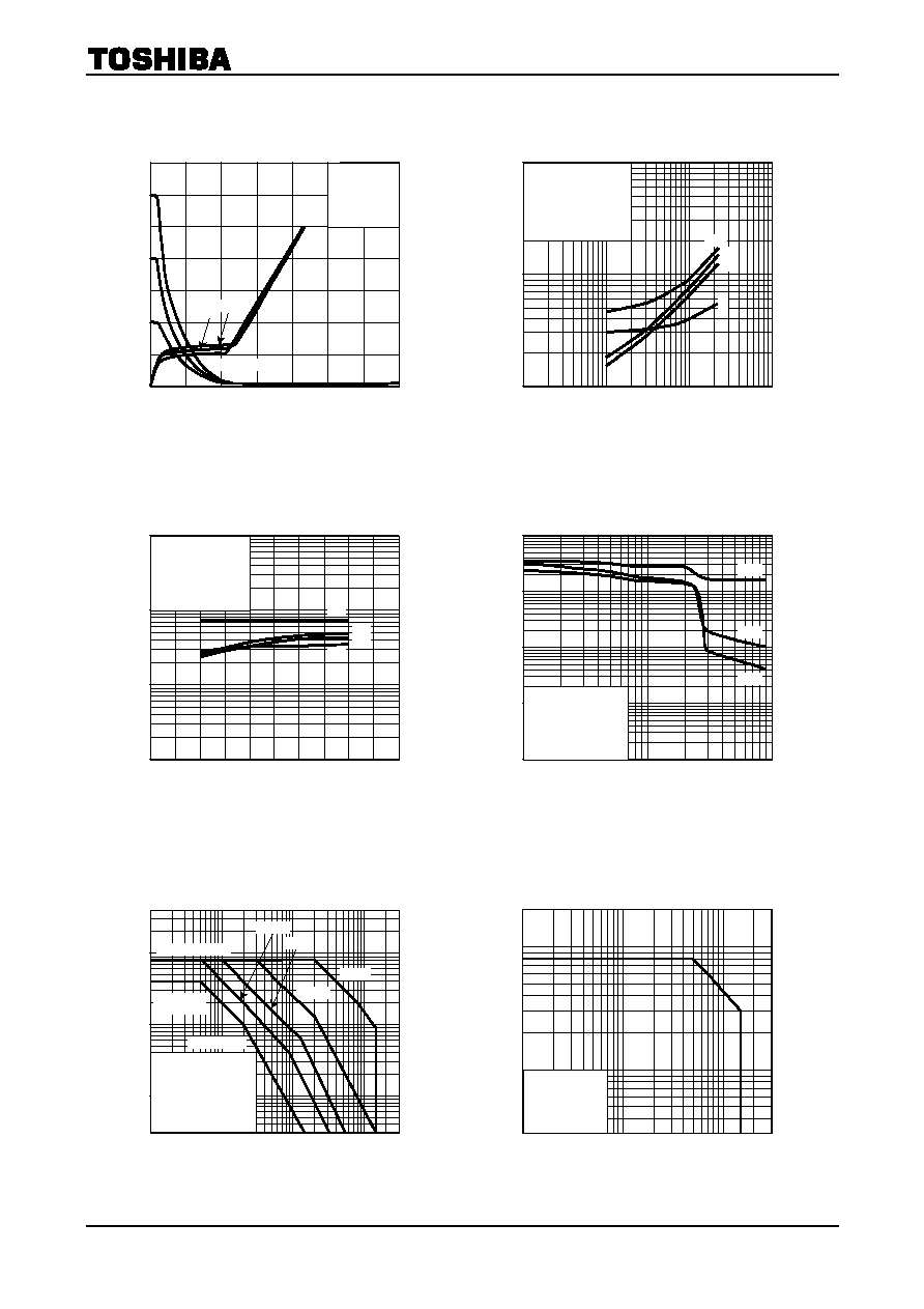
Case temperature Tc (∞C)
V
CE (sat)
≠ Tc
C
o
l
l
e
ct
or
-em
i
tte
r s
a
tu
rati
on
vol
t
age
V
CE (sat)
(V
)
10
8
6
4
2
0
0 4 8 12 16
20
80
Common emitter
Tc
=
-
40∞C
IC
=
10 A
60
40
20
10
8
6
4
2
0
0 4 8 12 16
20
20
Common emitter
Tc
=
25∞C
IC
=
10 A
40
60
80
10
8
6
4
2
0
0 4 8 12 16
20
20
Common emitter
Tc
=
125∞C
IC
=
10 A
40
60
80
100
80
60
40
20
0
0 4 8 12 16
20
25
Common emitter
VCE
=
5 V
Tc
=
125∞C
-
40
6
0
-
80
-
40 0 40
120
160
80
2
4
8
10
IC
=
10 A
Common emitter
VGE
=
15 V
20
40
60
80
100
80
60
40
20
0
0 2 4 6 8 10
VGE
=
8 V
10
12
15
20
25
GT40T301
2002-01-18
4
0
0 80
160
240
10
20
30
Common
emitter
RL
=
7.5
Tc
=
25∞C
VCE
=
100 V
200
300
40 120 200 280
0.1
1
0.3
0.5
1
3
5
10
3 5 10
30 50 100
300
500
1000
Common emitter
VCC
=
600 V
IC
=
40 A
VGG
=
±
15 V
Tc
=
25∞C
tf
tr
toff
ton
Co
lle
ct
o
r
cu
r
r
e
n
t
I
C
(A
)
C
apa
ci
ta
nce
C
(
p
F)
Gate charge Q
G
(nC)
V
CE
, V
GE
≠ Q
G
Co
lle
ct
o
r
-
e
m
i
tte
r
v
o
lta
g
e
V
CE
(
◊
10 V
)
Gate
-em
i
tt
er
volt
age
V
GE
(V
)
Gate
resistance R
G
(
)
Switching time ≠ R
G
Sw
itc
h
in
g
tim
e
(
µ
s)
Collector current I
C
(A)
Switching time ≠ I
C
Sw
itc
h
in
g
tim
e
(
µ
s)
Collector-emitter voltage V
CE
(V)
C ≠ V
CE
Collector-emitter voltage V
CE
(V)
Safe operating area
Collector-emitter voltage V
CE
(V)
Reverse bias SOA
Co
lle
ct
o
r
cu
r
r
e
n
t
I
C
(A
)
0.01
0 10 20 30 40 50
0.03
0.05
0.1
0.3
0.5
1
3
5
10
Common emitter
VCC
=
600 V
RG
=
51
VGG
=
±
15 V
Tc
=
25∞C
toff
tr
tf
ton
1
1 3
100
10000
5 10
30
50
3
5
10
30
50
100
300
500
1000
3000
5000
Cies
Coes
Cres
Common emitter
VGE
=
0 V
f
=
1 MHz
Tc
=
25∞C
0.3
3
0.5
1 10
30
100
300
1000
3000
1
3
5
10
30
50
100
300
*: Single nonrepetitive
pulse
Tc
=
25∞C
Curves must be derated
linearly with increase in
temperature.
DC operation
IC max (pulsed)*
IC max
(continuous)
10 ms*
1 ms*
100
µ
s*
10
µ
s*
3
10 30 100
300 1000
3000
10
30
100
200
Tj
<
=
125∞C
VGE
=
±
15 V
RG
=
51
GT40T301
2002-01-18
5
Reve
r
s
e
r
e
c
o
ve
r
y
tim
e
t
rr
(
µ
s)
Reve
r
s
e
r
e
c
o
ve
r
y
tim
e
t
rr
(
µ
s)
Emitter-collector forward current I
ECF
(A)
I
rr
, t
rr
≠ I
ECF
di/dt (A/
µ
s)
I
rr
, t
rr
≠ di/dt
2.5
2.0
1.5
1.0
0.5
0
100
80
60
40
20
0
0 40 80 120
160
240
200
Common collector
IECF
=
30 A
Tc
=
25∞C
Irr
trr
1.0
0.8
0.6
0.4
0.2
0
P
eak
rev
e
rs
e r
e
co
ver
y
cu
rr
ent
I
rr
(A
)
P
eak
rev
e
rs
e r
e
co
ver
y
cu
rr
ent
I
rr
(A
)
20
16
12
8
4
0
0 20 40 60 80 100
Common collector
di/dt
=
-
20 A/
µ
s
Tc
=
25∞C
Irr
trr
10
-
3
10
-
5
10
-
4
10
-
3
10
-
2
10
-
1
10
0
10
1
10
2
10
-
2
10
-
1
10
1
10
0
Tc
=
25∞C
Diode
IGBT
Pulse width t
w
(s)
R
th (t)
≠ t
w
T
r
ansi
e
nt t
h
e
r
m
a
l
i
m
pe
da
nce
R
th
(t)
(
∞
C
/
W
)
Emitter-collector forward voltage V
ECF
(V)
I
ECF
≠ V
ECF
E
m
itter-c
ollect
or
fo
r
w
a
r
d c
u
r
r
e
n
t
I
EC
F
(A
)
100
80
60
40
20
0
0 1 2 3 4 5
Common collector
Tc
=
40∞C
25
125
GT40T301
2002-01-18
6
∑
TOSHIBA is continually working to improve the quality and reliability of its products. Nevertheless, semiconductor
devices in general can malfunction or fail due to their inherent electrical sensitivity and vulnerability to physical
stress. It is the responsibility of the buyer, when utilizing TOSHIBA products, to comply with the standards of
safety in making a safe design for the entire system, and to avoid situations in which a malfunction or failure of
such TOSHIBA products could cause loss of human life, bodily injury or damage to property.
In developing your designs, please ensure that TOSHIBA products are used within specified operating ranges as
set forth in the most recent TOSHIBA products specifications. Also, please keep in mind the precautions and
conditions set forth in the "Handling Guide for Semiconductor Devices," or "TOSHIBA Semiconductor Reliability
Handbook" etc..
∑
The TOSHIBA products listed in this document are intended for usage in general electronics applications
(computer, personal equipment, office equipment, measuring equipment, industrial robotics, domestic appliances,
etc.). These TOSHIBA products are neither intended nor warranted for usage in equipment that requires
extraordinarily high quality and/or reliability or a malfunction or failure of which may cause loss of human life or
bodily injury ("Unintended Usage"). Unintended Usage include atomic energy control instruments, airplane or
spaceship instruments, transportation instruments, traffic signal instruments, combustion control instruments,
medical instruments, all types of safety devices, etc.. Unintended Usage of TOSHIBA products listed in this
document shall be made at the customer's own risk.
∑
The information contained herein is presented only as a guide for the applications of our products. No
responsibility is assumed by TOSHIBA CORPORATION for any infringements of intellectual property or other
rights of the third parties which may result from its use. No license is granted by implication or otherwise under
any intellectual property or other rights of TOSHIBA CORPORATION or others.
∑
The information contained herein is subject to change without notice.
000707EAA
RESTRICTIONS ON PRODUCT USE