
TOSHIBA
TOSHIBA
TOSHIBA
TOSHIBA
GT5J321
TOSHIBA Insulated Gate Bipolar Transistor Silicon N Chanenel IGBT
GT5J321
High Power Switching Applications
Fast Switching Applications
The 4th generation
Enhancement-mode
Fast Switching(FS)
:Operating frequency up to 150kHz(Reference)
High speed
:t
f
=0.05s(typ.)
Low switching loss :E
on
=0.12mJ(typ.)
:
E
off
=0.10mJ(typ.)
Low saturation voltage :V
CE(sat)
=2.0V(typ.)
FRD included between emitter and collector
Maximum Ratings (Ta=25)
Maximum Ratings (Ta=25)
Maximum Ratings (Ta=25)
Maximum Ratings (Ta=25)
Characteristic
Symbol
Ratings
Unit
Collector-emitter voltage
V
CES
600
V
Gate-emitter voltage
V
GES
�20
V
DC
I
C
5
1ms
I
CP
10
Emitter-collector
DC
I
F
5
forward current
1ms
I
FM
10
Collector power dissipation
(Tc=25)
Junction temperature
T
j
150
Storage temperature range
T
stg
-55150
2001-6- 1/6
Collector current
P
C
28
W
A
A
Preliminary
Preliminary
Preliminary
Preliminary
TOSHIBA
TOSHIBA
TOSHIBA
TOSHIBA
GT5J321
Electrical Characteristics(Ta=25)
Electrical Characteristics(Ta=25)
Electrical Characteristics(Ta=25)
Electrical Characteristics(Ta=25)
Test Condition
I
GES
V
GE
=�20V,V
CE
=0
�500
I
CES
V
CE
=600V,V
GE
=0
V
GE(OFF)
I
C
=0.5mA,V
CE
=5V
V
CE(sat)
I
C
=5A,V
GE
=15V
C
ies
V
CE
=10V,V
GE
=0,f=1MHz
Turn-on delay time
t
d(on)
Rise Time
t
r
Inductive Load
Turn-on Time
t
on
V
CC
=300V,I
C
=5A
Turn-off delay time
t
d(off)
V
GG
=+15V,R
G
=100
Fall Time
t
f
(Note 1)
Turn-off Time
t
off
(Note 2)
Turn-on switching loss
E
on
Turn-off switching loss
E
off
V
F
I
F
=5A,V
GE
=0
t
rr
I
F
=5A,di/dt=-100A/s
Thermal resistance(IGBT)
R
th(j-c)
Thermal resistance(Diode)
R
th(j-c)
2001-6- 2/6
-
-
4.90 /W
-
-
4.46 /W
V
Reverse recovery time
-
-
200
ns
Peak forward voltage
-
-
2.0
-
0.13
-
mJ
-
0.10
-
-
-
0.03
-
-
0.15
-
0.15
-
-
Switching time
-
Switching loss
-
-
0.05
0.20
Input capacitance
-
Collector-emitter saturation volatage
-
3.5
-
-
Min
Typ.
-
-
-
mA
V
6.5
Max
1.0
0.12
Unit
Gate leakage current
Collector cut-off current
Characteristic
Symbol
Gate-emitter cut-off voltage
-
2.0
nA
2.45
V
-
950
0.05
pF
s
Preliminary
Preliminary
Preliminary
Preliminary

TOSHIBA
TOSHIBA
TOSHIBA
TOSHIBA
GT5J321
2001-6- 3/6
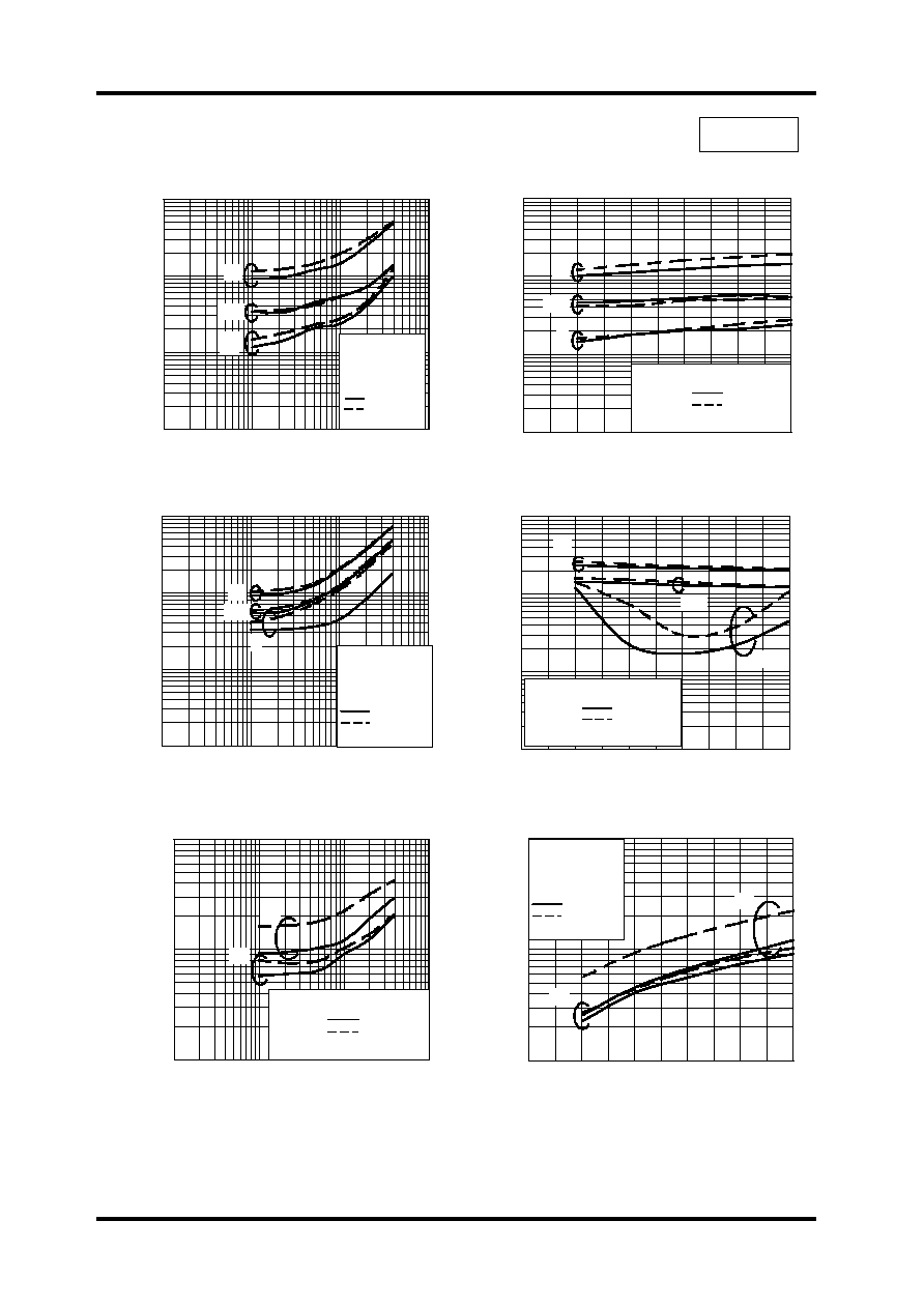
I
C
- V
GE
0
2
4
6
8
10
0
2
4
6
8
10
12
14
Gate-emitter voltageV
GE
(V)
C
o
l
l
e
ct
o
r
cu
rr
ent
I
C
(A
)
-40
Tc = 25
125
Common emitter
V
CE
CE
CE
CE
= 5V
V
CE(sat)
- T
c
0
1
2
3
4
-60
-20
20
60
100
140
Case tenpera
c
()
C
o
l
l
e
ct
or
-e
m
i
tt
er
s
a
tu
ra
ti
o
n
v
o
l
t
a
g
e
V
CE
(
s
a
t
)
(V
)
10
5
I
C
= 2A
Common emitter
V
GE
GE
GE
GE
= 15V
V
CE
- V
GE
0
4
8
12
16
20
0
4
8
12
16
20
Gate-emitter voltageV
GE
(V)
Co
lle
c
t
o
r
-
e
m
i
t
t
e
r
v
o
lt
a
g
e
V
CE
(V
)
Common emitter
Tc
= -40
V
CE
- V
GE
0
4
8
12
16
20
0
4
8
12
16
20
Gate-emitter voltageV
GE
(V)
C
o
ll
e
c
t
o
r
-
e
m
it
t
e
r
v
o
lt
a
g
e
V
CE
(V
)
Common emitter
Tc
= 125
10
5
I
C
= 2A
20
10
I
C
= 5A
V
CE
- V
GE
0
4
8
12
16
20
0
4
8
12
16
20
Gate-emitter voltageV
GE
(V)
C
o
llect
o
r
-em
it
t
e
r
v
o
lt
a
g
e
V
CE
(V
)
Common emitter
Tc
= 25
10
5
I
C
= 2A
I
C
- V
CE
0
2
4
6
8
10
0
1
2
3
4
5
Collector-emitter voltageV
CE
(V)
C
o
l
l
ect
o
r
cu
rr
en
t
I
C
(A
)
Common
emitte
Tc
= 25
20
15
10
9
V
GE
= 8V
Reference
Case temperature Tc ()
TOSHIBA
TOSHIBA
TOSHIBA
TOSHIBA
GT5J321
2001-6- 4/6
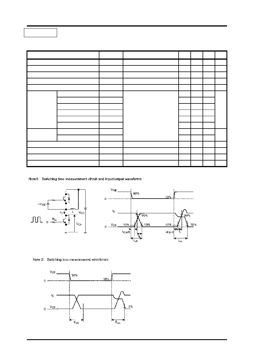
Switching time t
off
, t
f
, t
d(off)
- R
G
0.001
0.01
0.1
1
1
10
100
1000
Gate resistanceR
G
()
S
w
it
c
h
in
g
t
i
m
e
t
of
f
, t
f
t
d
(
o
ff)
(
s)
t
f
t
d(off)
t
off
Switching lossE
on
, E
off
- R
G
0.01
0.1
1
1
10
100
1000
Gate resistanceR
G
()
S
w
it
c
h
i
n
g
lo
s
s
E
on
, E
of
f
(m
J)
E
on
E
off
Switching time
on
, t
r
, t
d(on)
- I
C
0.001
0.01
0.1
1
0
1
2
3
4
5
Collector currentI
C
(A)
S
w
it
c
h
in
g
t
i
m
e
t
on
, t
r
, t
d(
o
n
)
(
s)
t
on
t
d(on)
t
r
Switc h
i
off
, t
f
, t
d(off)
- I
C
0.001
0.01
0.1
1
0
1
2
3
4
5
Collector currentI
C
(A)
Sw
it
c
h
in
g
t
i
m
e
t
of
f
, t
f
, t
d
(
o
ff)
(
s)
t
f
t
d(off)
t
off
Common emitter
V
C C
C C
C C
C C
=300V
V
G G
G G
G G
G G
=15V
R
G
G
G
G
=100
Tc=25
Tc=125
Note1
Switching lossE
on
, E
off
- I
C
0.01
0.1
1
0
1
2
3
4
5
Collector currentI
C
(A)
S
w
i
t
c
h
in
g l
o
ss
E
on
, E
of
f
(m
J
)
E
on
E
off
Switching time
on
, t
r
, t
d(on)
- R
G
0.001
0.01
0.1
1
1
10
100
1000
Gate resistanceR
G
()
S
w
i
t
chi
n
g
ti
m
e
t
on
, t
r
, t
d(
o
n
)
(
s)
t
on
t
d(on)
t
r
Common emitter
V
CC
CC
CC
CC
=300V
V
GG
GG
GG
GG
=15V
I
C
C
C
C
=5A
Tc=25
Tc=125
Note1
Common emitter
V
CC
CC
CC
CC
=300V
V
GG
GG
GG
GG
=15V
I
C
C
C
C
=5A
Tc=25
Tc=125
Note1
Common emitter
V
CC
CC
CC
CC
=300V
V
GG
GG
GG
GG
=15V
R
G
G
G
G
=100
Tc=25
Tc=125
Note2
Reference
Common emitter
V
CC
CC
CC
CC
=300V
V
GG
GG
GG
GG
=15V
R
G
G
G
G
=100
Tc=25
Tc=125
Note
Common emitter
V
CC
CC
CC
CC
=300V
V
GG
GG
GG
GG
=15V
I
C
C
C
C
=5A
Tc=25
Tc=125
Note2
Switching time t
on
,t
r
,t
d(on)
- R
G
Switching time t
on
,t
r
,t
d(on)
- I
C
Switching time t
off
,t
f
,t
d(off)
- R
G
Switching time t
off
,t
f
,t
d(off)
- I
C

TOSHIBA
TOSHIBA
TOSHIBA
TOSHIBA
GT5J321
2001-6- 5/6
V
CE
, V
GE
- Q
G
0
100
200
300
400
500
0
10
20
30
40
Gate chargeQ
G
(nC)
C
o
l
l
e
c
tor
e
m
i
tte
r
v
o
l
t
ag
e
VC
E
(V
)
0
4
8
12
16
20
G
ate
-
e
m
i
t
te
r vo
l
t
a
g
e
V
GE
(V
)
V
CE
=300V
100
200
t
rr
, I
rr
- I
F
1
10
100
0
2
4
6
8
10
Forward currentI
F
(A)
R
e
v
e
rs
e rec
o
v
e
ry
cur
rent
I
rr
(A
)
10
100
1000
R
e
v
e
r
s
e r
eco
v
e
r
y
t
i
m
e
t
rr
(ns
)
I
rr
t
rr
C-V
CE
1
10
100
1000
0.1
1
10
100
1000
Collector-emitter voltageV
CE
(V)
Ca
p
a
c
i
tan
c
e
C (
p
F
)
I
F
-V
F
0
4
8
12
16
20
0
0.4
0.8
1.2
1.6
2
Forward voltageV
F
(V)
F
o
rw
a
r
d
cu
rrent
I
F
(A
)
-40
Tc=25
125
Common collector
V
GE
GE
GE
GE
=0
Common collector
di/dt=-100A/s
V
GE
GE
GE
GE
=0
Tc=25
Tc=125
C
ies
C
oes
C
res
Common emitter
V
GE
GE
GE
GE
=0
f=1MHz
Tc=25
Reference
Safe operati
0.1
1
10
100
1
10
100
1000
Collector-emitter voltage V
CE
(V)
C
o
l
l
e
c
t
o
r
cu
rrent
I
C
(
A
)
1 0 ms
1 0 ms
1 0 ms
1 0 ms
*
*
*
*
1 ms
1 ms
1 ms
1 ms
*
*
*
*
1 0 0 s
1 0 0 s
1 0 0 s
1 0 0 s
*
*
*
*
5 0 s
5 0 s
5 0 s
5 0 s
*
*
*
*
Common emitter
R
L
L
L
L
=60
Tc=25
Reverse bias SOA
0.1
1
10
100
1
10
100
1000
Collector-emitter voltage V
CE
(V)
C
o
l
l
e
c
t
o
r
cu
rrent
I
C
(
A
)
Tj125
V
GE
GE
GE
GE
=15V
R
G
G
G
G
=13
Safe operating area
*
Single nonrepetitive
pulse Tc=25
Curves must be dilated
linearly with increase in
temperature.
DC
operation
Ic max (continuous)
Ic max (pulsed)
*
Tj125
V
GE
GE
GE
GE
=15V
R
G
G
G
G
=100