(1/10) 1999-10-14 (Ver.3.2)
LIQUID CRYSTAL DISPLAY DIVISION
PRODUCT INFORMATION
FEATURES
(1) 10.4"XGA display size for notebook PC
(2) LVDS interface system
(3) Slim(5.5mmMAX) & light weight(265gTYP) design
MECHANICAL SPECIFICATIONS
Item
Specifications
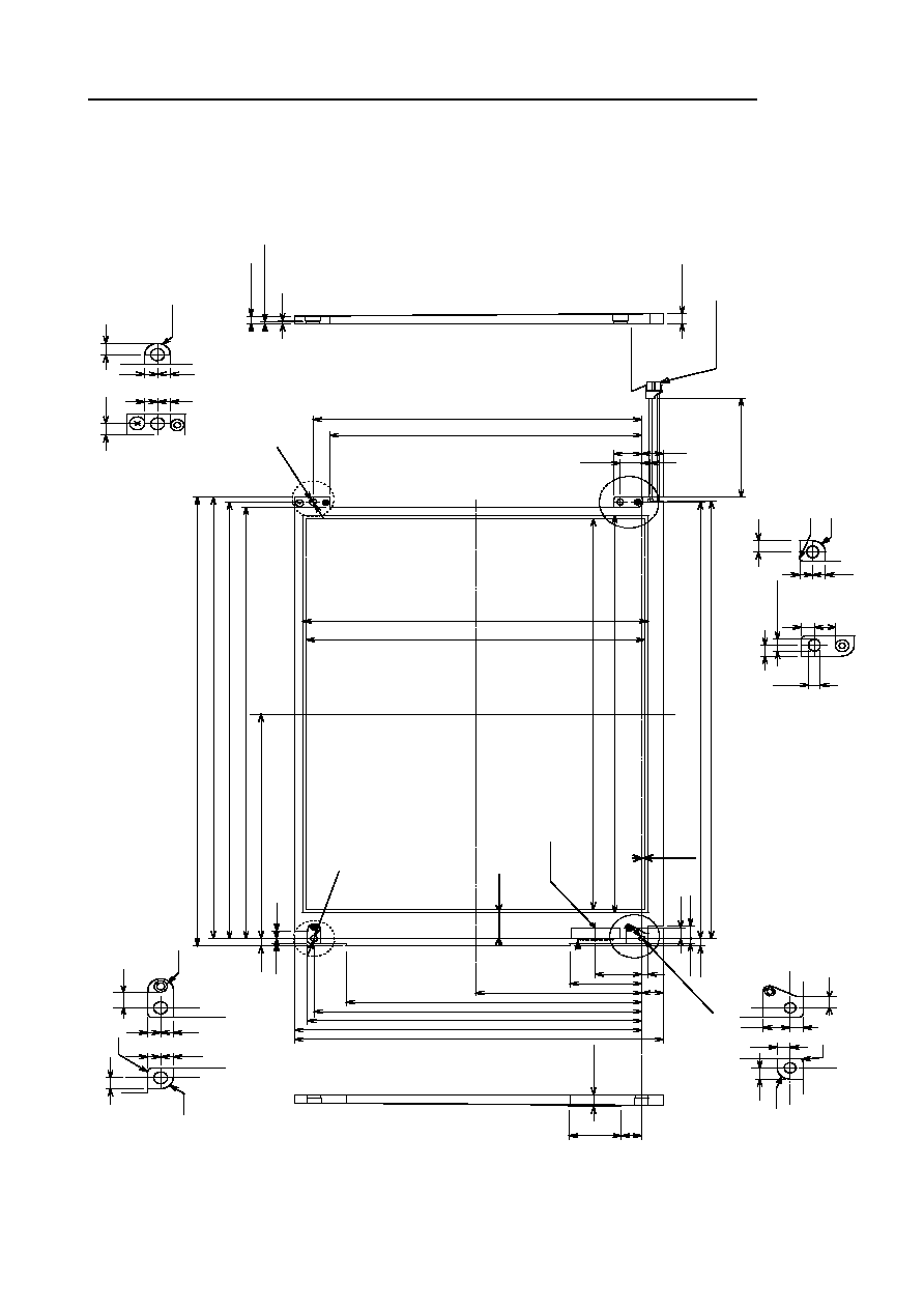
Dimensional Outline (Typ.)
241.5(W) x 171.9(H) x 5.5max(D) mm
Number of Pixels
1024(W) x 768(H) pixels
Active Area
210.432(W) x 157.824(H) mm
Pixel Pitch
0.2055(W) x 0.2055(H)
Weight (approximately)
265g
Backlight
Single CCFL, Sidelight type
ABSOLUTE MAXIMUM RATINGS
Item
Min.
Max.
Unit
(V
DD
)
-0.3
4.5
V
Supply Voltage
(V
FL
)
0
2.0
kV(rms)
FL Driving Frequency (f
FL
)
-
100
kHz
Input Signal Voltage (V
IN
)
-0.3
V
DD
+0.3
V
Operating Temperature
0
50
∞
C
Storage Temperature
-20
60
∞
C
Storage Humidity
10
90
%(RH)
ELECTRICAL SPECIFICATION
Item
Min.
Typ.
Max.
Unit
Remarks
(V
DD
)
3.0
3.3
3.6
V
Supply Voltage
(V
FL
)
600
650
700
V(rms)
I
FL
=2.5 mA(rms)
FL Start Voltage (Ta=0
∞
C)
1200
---
1600
V(rms)
Receiver Input Voltage
0
---
2.4
V
Differential Input High Threshold(V
TH
)*1
---
---
V
OS
+0.1
V
Differential Input Low Threshold(V
TL
)*1
V
OS
-0.1
---
---
V
V
OS
:Offset Mode Voltage
V
OS
=1.2V
*2 (I
DD
)
---
360
---
mA
Current Consumption
*3 (I
FL
)
2.0
2.5
5.0
mA(rms)
*2 *3 Power Consumption
---
2.8
---
W
@70cd/m
2
*1 : Refer to DF90CF364 Specification by National Semiconductor Corporation. This LCD module conforms to LVDS
standard (TIA/EIA-644)
*2 : 8 color bars pattern
*3 : Excepting the efficiency FL inverter
*4 : not use Hsync nor Vsync. Only ENAB control.
OPTICAL SPECIFICATION (Ta=25
∞
C)
Item
Min.
Typ.
Max.
Unit
Remarks
Contrast Ratio (CR)
100
250
---
---
(t
ON
)
---
---
50
ms
Response Time
(t
OFF
)
---
---
50
ms
50
70
---
cd/m
2
I
FL
=2.5mA(rms)
Luminance (L)
---
200
---
cd/m
2
I
FL
=5mA(rms)
*The information contained herein is presented only as a guide for the applications of our products. No responsibility is assumed by
Toshiba or other rights of the third parties which may result from its use. No license is granted by implication or otherwise under any
patent or patent rights of Toshiba or others.
*The information contained herein may be changed without prior notice. It is therefore advisable to contact Toshiba before
proceeding with the design of equipment incorporating this product.
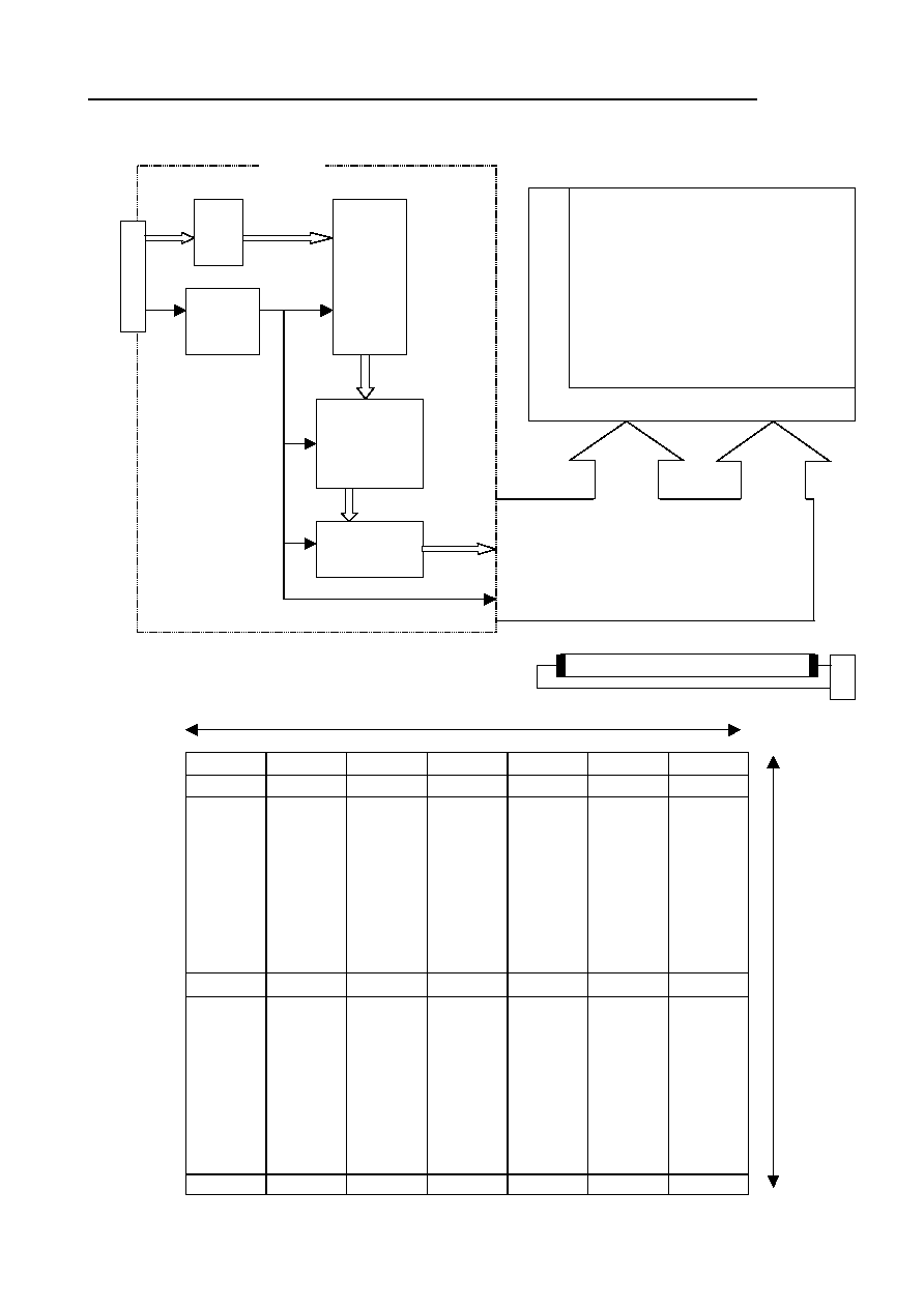
26cm COLOUR TFT-LCD MODULE
(10.4 TYPE)
LTM10C306L
(p-Si TFT)
TENTATIVE
(5/10) 1999-10-14 (Ver.3.2)
LTM10C306L
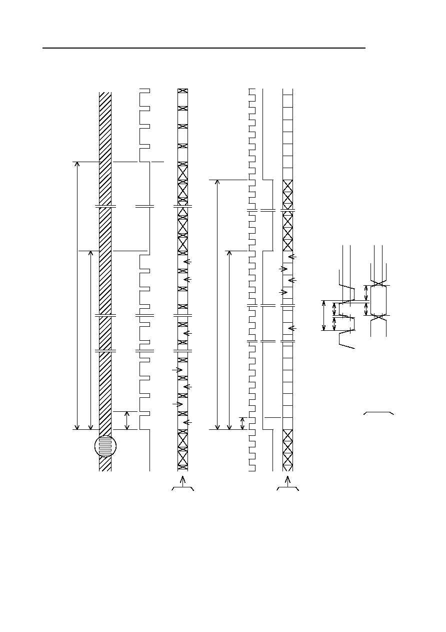
TIMING SPECIFICATION
1)2)3)4)5)6)
Item
Symbol
Min.
Typ.
Max.
Unit
Remarks
Frame Period
t1
778
◊
t3
-
806
◊
t3
16.67
860
◊
t3
17.25
-
ms
Vertical
Display Term
t2
768
◊
t3
768
◊
t3
768
◊
t3
-
One Line Scanning
Time
t3
1319
◊
t5
20.04
1344
◊
t5
20.68
1462
◊
t5
-
-
µ
s
Horizontal
Display Term
t4
1024
◊
t5
1024
◊
t5
1024
◊
t5
-
Clock Period
t5
15.0
15.38
-
ns
Note 1) Refer to "TIMING CHART" and LVDS (DF90CF364MTD) specifications by National Semiconductor.
Note 2) If ENAB is fixed to "H" or "L" level for certain period while NCLK is supplied, the panel displays black with some
flicker.
Note 3) If NCLK is fixed to "H" or "L" level for certain period while ENAB is supplied, the panel may be damaged.
Note 4) Please adjust LCD operating signal timing and FL driving frequency, to optimize the display quality.
There is a possibility that flicker is observed by the interference of LCD operating signal timing and FL driving
Condition (especially driving frequency ), even if the condition satisfies above timing specifications and
recommended operating conditions shown in 3.
Note 5) Do not make t1,t2 and t3 fluctuate.
If t1,t2 and t3 are fluctuate, the panel displays black.
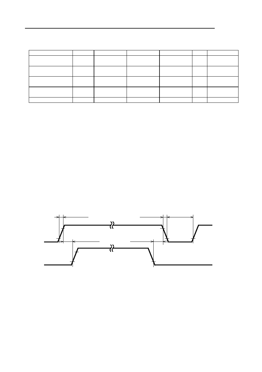
SEQUENCE OF POWER SUPPLIES AND SIGNALS
DD
NCLK
DATA
ENAB
3.0V
3.0V
0.2V
0.2V
0.2V
DD
500ms(min.)
10ms(max.)
40ms(max.)
10ms(max.)
40ms(max.)
0ms(min.)
0.2 V
V
0ms(min.)
DD
0.2 V