 | –≠–ª–µ–∫—Ç—Ä–æ–Ω–Ω—ã–π –∫–æ–º–ø–æ–Ω–µ–Ω—Ç: MP4412 | –°–∫–∞—á–∞—Ç—å:  PDF PDF  ZIP ZIP |
MP4412
2004-07-01
1
TOSHIBA Power MOS FET Module Silicon N Channel MOS Type (Four L
2
--MOSV inOne)
MP4412
High Power, High Speed Switching Applications
For Printer Head Pin Driver and Pulse Motor Driver
For Solenoid Driver
∑ 4-V gate drivability
∑ Small package by full molding (SIP 12 pins)
∑ High drain power dissipation (4-device operation)
:
P
T
= 28 W (Tc = 25∞C)
∑ Low drain-source ON resistance: R
DS (ON)
= 0.17 (typ.)
∑ High forward transfer admittance: |Y
fs
| = 4.5 S (typ.)
∑ Low leakage current: I
GSS
= ±10 µA (max) (V
GS
= ±16 V)
I
DSS
= 100 µA (max) (V
DS
= 100 V)
∑ Enhancement-mode: V
th
= 0.8 to 2.0 V (V
DS
= 10 V, I
D
= 1 mA)
Maximum Ratings
(Ta = 25∞C)
Characteristics Symbol
Rating
Unit
Drain-source voltage
V
DSS
100 V
Drain-gate voltage (R
GS
= 20 k) V
DGR
100 V
Gate-source voltage
V
GSS
±20 V
DC I
D
5
Drain current
Pulse I
DP
20
A
Drain power dissipation
(1-device operation, Ta = 25∞C)
P
D
2.2 W
Ta = 25∞C
4.4
Drain power dissipation
(4-device operation)
Tc = 25∞C
P
DT
28
W
Single Pulse avalanche energy
(Note
1)
E
AS
180
mJ
Avalanche current
I
AR
5 A
1-device
operation
E
AR
0.22
Repetitive avalanche
energy (Note
2)
4-device
operation
E
ART
0.44
mJ
Channel temperature
T
ch
150
∞C
Storage temperature range
T
stg
-55 to 150
∞C
Note 1: Condition for avalanche energy (single pulse) measurement
V
DD
= 25 V, starting T
ch
= 25∞C, L = 11.6 mH, R
G
= 25 , I
AR
= 5 A
Note 2: Repetitive rating; pulse width limited by maximum channel temperature.
This transistor is an electrostatic-sensitive device. Please handle with caution.
Industrial Applications
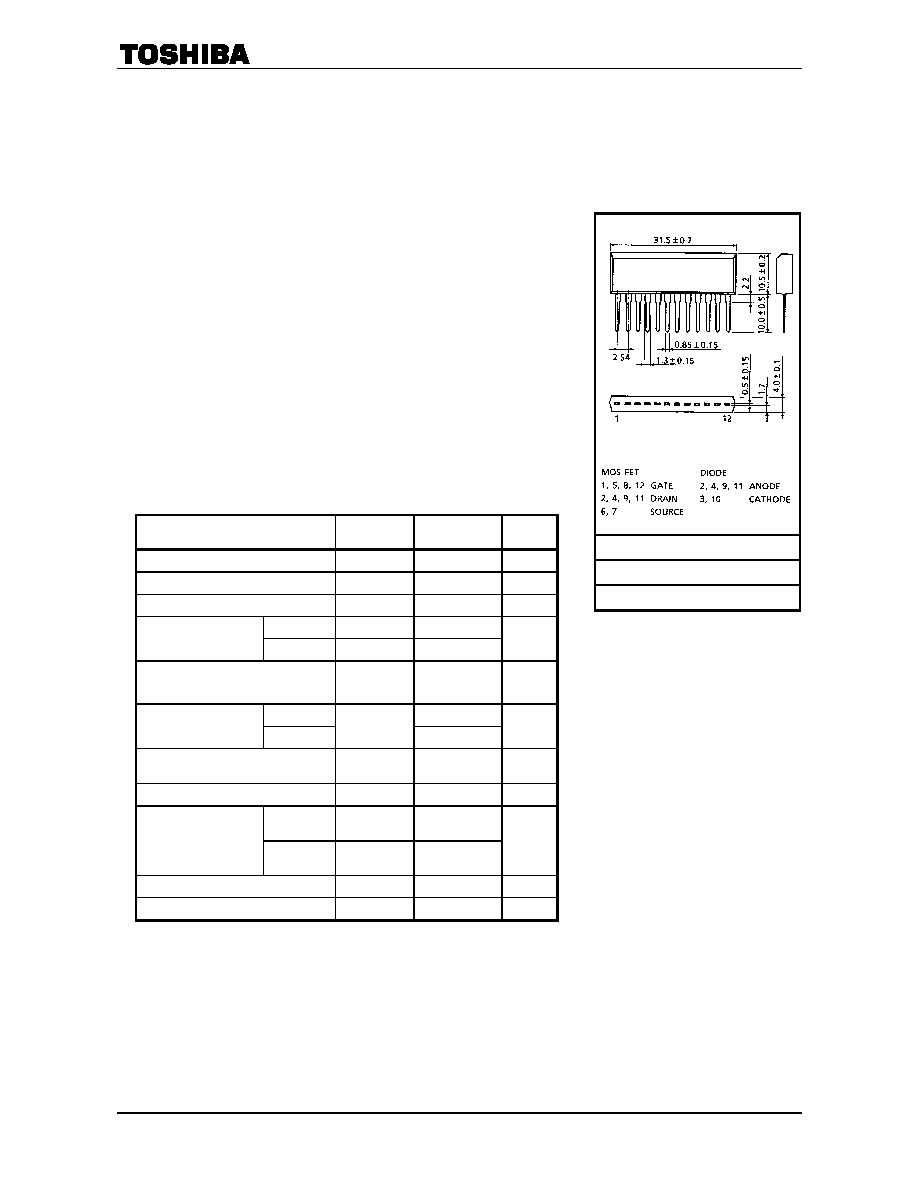
Unit: mm
JEDEC
JEITA
TOSHIBA 2-32C1D
Weight: 3.9 g (typ.)
MP4412
2004-07-01
2
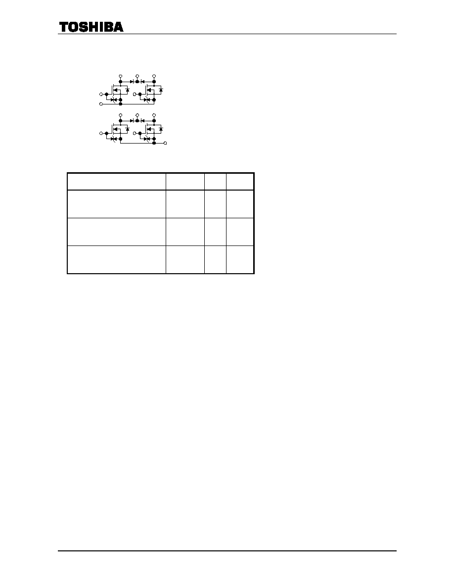
Array Configuration
Thermal Characteristics
Characteristics Symbol
Max
Unit
Thermal resistance from channel to
ambient
(4-device operation, Ta = 25∞C)
R
th (ch-a)
28.4
∞C/W
Thermal resistance from channel to
case
(4-device operation, Tc = 25∞C)
R
th (ch-c)
4.46
∞C/W
Maximum lead temperature for
soldering purposes
(3.2 mm from case for t = 10 s)
T
L
260
∞C
5
4
2 3
1
6
12
11
9 10
8
7

MP4412
2004-07-01
3
Electrical Characteristics
(Ta = 25∞C)
Characteristics Symbol Test
Condition Min
Typ.
Max
Unit
Gate leakage current
I
GSS
V
GS
= ±16 V, V
DS
= 0 V
±10 µA
Drain cut-off current
I
DSS
V
DS
= 100 V, V
GS
= 0 V
100 µA
Drain-source breakdown voltage
V
(BR) DSS
I
D
= 10 mA, V
GS
= 0 V
100
V
Gate threshold voltage
V
th
V
DS
= 10 V, I
D
= 1 mA
0.8
2.0 V
V
GS
= 4 V, I
D
= 2.5 A
0.22 0.30
Drain-source ON resistance
R
DS (ON)
V
GS
= 10 V, I
D
= 2.5 A
0.17 0.23
Forward transfer admittance
|Y
fs
|
V
DS
= 10 V, I
D
= 2.5 A
2.0
4.5
S
Input capacitance
C
iss
500 pF
Reverse transfer capacitance
C
rss
80 pF
Output capacitance
C
oss
V
DS
= 10 V, V
GS
= 0 V
f = 1 MHz
190 pF
Rise time
t
r
17
Turn-on time
t
on
25
Fall time
t
f
50
Switching time
Turn-off time
t
off
V
IN
: t
r
, t
f
< 5 ns, duty 1%, t
w
= 10 µs
195
µs
Total gate charge
(gate-source plus gate-drain)
Q
g
22 nC
Gate-source charge
Q
gs
15 nC
Gate-drain ("miller") charge
Q
gd
V
DD
80 V, V
GS
= 10 V
I
D
= 5 A
7 nC
Source-Drain Diode Ratings and Characteristics
(Ta = 25∞C)
Characteristics Symbol Test
Condition Min
Typ.
Max
Unit
Continuous drain reverse current
I
DR
5 A
Pulse drain reverse current
I
DRP
20 A
Diode forward voltage
V
DSF
I
DR
= 5 A, V
GS
= 0 V
-1.7 V
Reverse recovery time
t
rr
160 ns
Reverse recovery charge
Q
rr
I
DR
= 5 A, V
GS
= 0 V
dI
DR
/dt = 50 A/µs
0.28 µC
Flyback-Diode Rating and Characteristics
(Ta = 25∞C)
Characteristics Symbol Test
Condition Min
Typ.
Max
Unit
Forward current
I
FM
5 A
Reverse current
I
R
V
R
= 100 A
0.4 µA
Reverse voltage
V
R
I
R
= 100 µA
100
V
Forward voltage
V
F
I
F
= 2 A
2.3 V
10
V
V
GS
R
L
= 2
0
V
DD
50 V
I
D
= 2.5
A
V
OUT
50
0 V

MP4412
2004-07-01
4
Marking
MP4412
JAPAN
Lot No.
A line indicates
lead (Pb)-free package or
lead (Pb)-free finish.
Part No. (or abbreviation code)
MP4412
2004-07-01
5
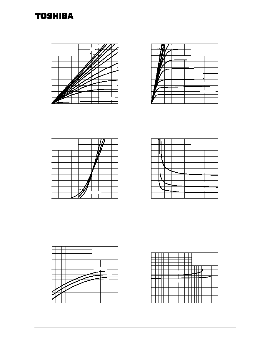
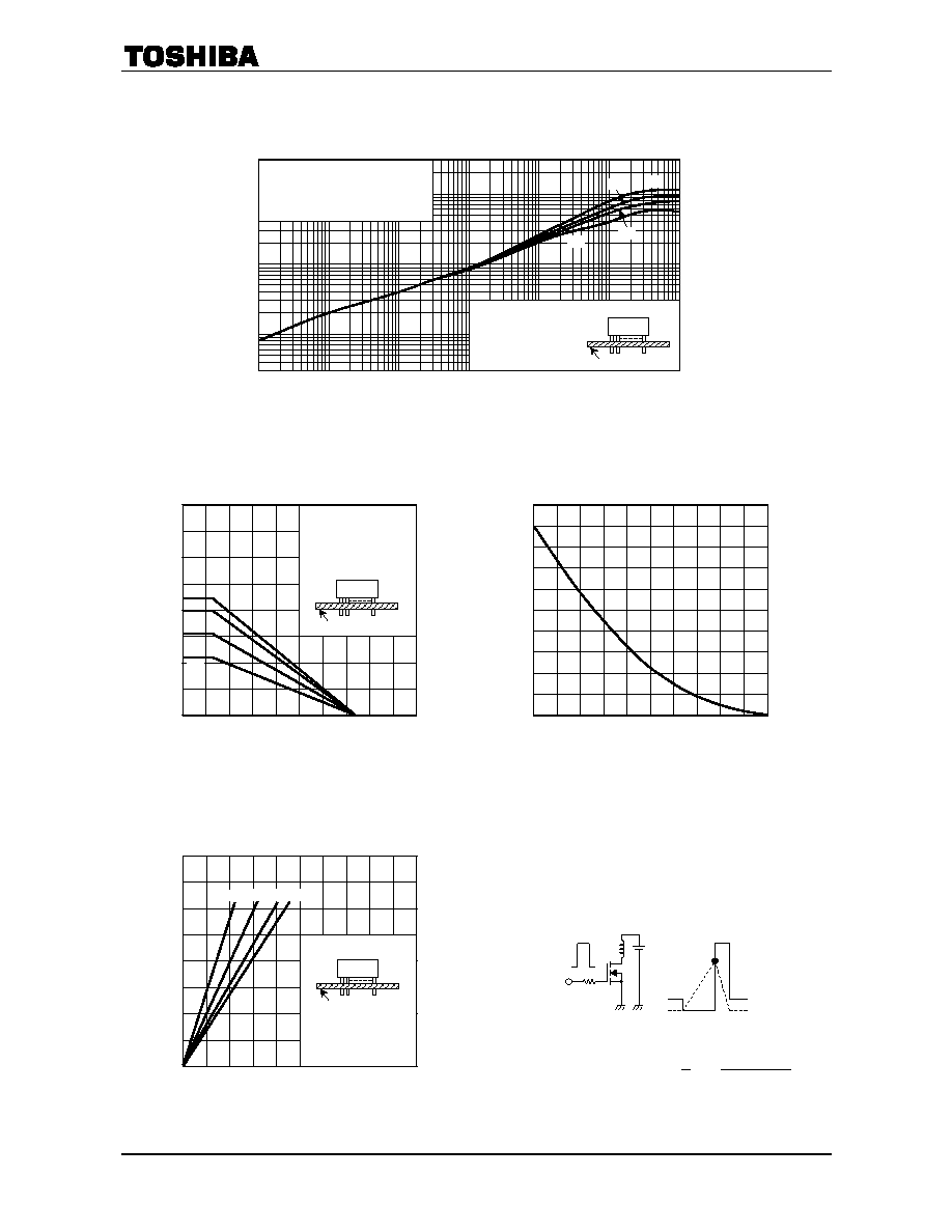
Drain current ID (A)
|Y
fs
|
≠ I
D
Fo
rwar
d t
r
a
n
sfe
r
ad
mi
ttanc
e
|
Y
fs
|
(S)
Drain current ID (A)
R
DS (ON)
≠ I
D
Drain-source voltage VDS (V)
I
D
≠ V
DS
D
r
ain
cu
rre
nt
I D
(A)
Drain-source voltage VDS (V)
I
D
≠ V
DS
D
r
ain
cu
rre
nt
I D
(A)
Gate-source voltage VGS (V)
I
D
≠ V
GS
Dr
a
i
n c
u
r
r
en
t
I D
(A)
Gate-source voltage VGS (V)
V
DS
≠ V
GS
Dr
ai
n-
s
o
u
r
ce
vo
lt
ag
e
V
DS
(V
)
)
Drain
-
s
o
urc
e
O
N
re
sistanc
e
R
DS
(
O
N)
(
)
0
0
Common source
Tc = 25∞C
1
2
3
4
5
0.2 0.4 0.6 0.8 1.0
3
VGS = 2.0 V
2.6
2.8
5
3.5
4
2.4
6
8
10
0
0
Common source
VDS = 10 V
100
25
Tc = -55∞C
2
4
6
8
10
1 2 3 4 5
0
0
Common source
Tc = 25∞C
ID = 5 A
2.5
1.3
0.4
0.8
1.2
1.6
2.0
4 8 12
16
20
0.3
0.03
0.05
0.1
0.3
1.0
0.5 1
3
5 10
30
Common source
Tc = 25∞C
VGS = 4 V
10
0.5
0
0
Common source
Tc = 25∞C
2
4
6
8
10
2 4 6 8 10
3.5
VGS = 2.5 V
3
3.25
5
3.75
4
2.75
6
8
10
0.3
1
100
25
Tc = -55∞C
Common source
VDS = 10 V
3
5
10
30
50
0.5 1
3
5 10
30
MP4412
2004-07-01
6
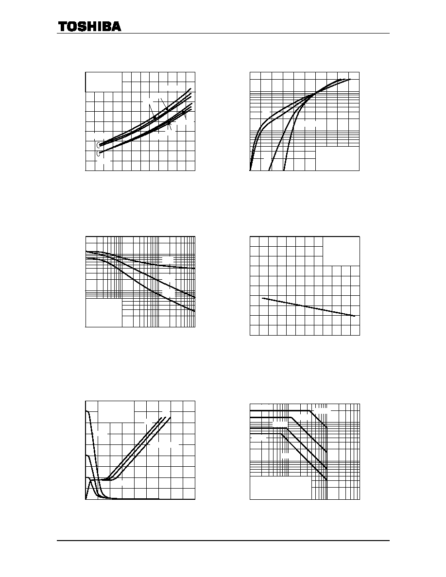
Case temperature Tc (∞C)
R
DS (ON)
≠ Tc
D
r
ai
n
-
so
urc
e
on resi
s
t
a
n
ce
R
DS (ON)
(
)
Drain-source voltage VDS (V)
I
DR
≠ V
DS
Drain
re
v
e
r
s
e c
u
r
r
e
n
t
I DR
(
A
)
Case temperature Tc (∞C)
V
th
≠ Tc
Gate
th
res
hol
d vol
t
a
g
e
V
th
(
V
)
Drain-source voltage VDS (V)
Capacitance ≠ V
DS
C
apaci
t
anc
e
C
(
p
F)
Gate
-so
u
r
c
e
v
o
ltage
V
GS
(
V
)
Total gate charge Qg (nC)
Dynamic Input/Output Characteristics
Dr
ai
n-
s
o
u
r
ce
vo
lt
ag
e
V
DS
(V
)
Drain-source voltage VDS (V)
Safe Operating Area
D
r
ain
cu
rre
nt I
D
(A)
Common source
VGS = 0 V
f = 1 MHz
Tc = 25∞C
10
0.1
0.3 0.5
1
3 5
10
30 50 100
30
50
100
300
500
1000
3000
Ciss
Coss
Crss
0
0
0
Common source
ID = 5 A
Tc = 25∞C
8 16 24 32
20
40
60
80
4
8
12
16
VDD = 80 V
20
40
VDS
VGS
0
-80
Common source
VDS = 10 V
ID = 1 mA
-40 0 40 80 120 160
1
2
3
4
5
0.1
1
100 µs*
10 ms*
1 ms*
ID max
100 ms*
3 10 30
100
300
0.3
1
3
10
30
*: Single nonrepetitive pulse
Tc = 25∞C
Curves must be derated linearly
with increase in temperature.
IDP max
0
-80
-40 0 40 80 120 160
0.1
0.2
0.3
0.4
0.5
VGS = 4 V
10 V
1.3
ID = 5 A
1.3
2.5
2.5
ID = 5 A
Common source
Common source
Tc = 25∞C
0.1
0
-0.4
-0.8
-1.2
-1.6
-2.0
0.3
0.5
1
3
5
10
30
VGS = 0, -1 V
10
3
1
MP4412
2004-07-01
7
r
th
≠ t
w
T
r
a
n
sie
n
t t
h
e
r
m
a
l
res
i
stanc
e
r th
(∞
C/
W
)
Ambient temperature Ta (∞C)
P
DT
≠ Ta
T
o
t
a
l
po
wer
di
ssi
p
a
ti
on
P
DT
(W
)
T
ch
≠ P
DT
Chan
n
e
l te
mp
era
t
u
r
e
i
n
c
r
eas
e
T
ch
(∞
C)
Channel temperature Tch (∞C)
E
AS
≠ T
ch
A
v
al
anc
he
en
er
gy
E
AS
(m
J)
)
Total power dissipation PDT (W)
Pulse width tw (s)
0
8
40
2
4
6
80
120
160
200
0
(1) 1-device operation
(2) 2-device operation
(3) 3-device operation
(4) 4-device operation
Attached on a circuit board
Circuit board
(4)
(3)
(2)
(1)
Attached on a circuit board
(1) 1-device operation
(2) 2-device operation
(3) 3-device operation
(4) 4-device operation
2 4 6
8
0
160
40
80
120
10
0
Circuit board
(1) (2) (3) (4)
0.001 0.01 0.1
1
10 100 1000
Curves should be applied in thermal
limited area. (Single nonrepetitive pulse)
The figure shows thermal resistance per
device versus pulse width.
-No heat sink/Attached on a circuit board-
(1) 1-device operation
(2) 2-device operation
(3) 3-device operation
(4) 4-device operation
Circuit board
(1)
(2)
(3)
(4)
0.3
1
3
10
30
100
300
0
25
40
80
120
160
200
50 75 100
125 150
TEST CIRCUIT
TEST WAVE FORM
I
AR
B
VDSS
V
DD
V
DS
Peak I
AR
= 5 A, R
G
= 25
V
DD
= 25 V, L = 11.6 mH
-15
V
15
V
-
=
DD
VDSS
VDSS
2
AS
V
B
B
∑
∑L∑I
2
1

MP4412
2004-07-01
8
∑ The information contained herein is subject to change without notice.
∑ The information contained herein is presented only as a guide for the applications of our products. No
responsibility is assumed by TOSHIBA for any infringements of patents or other rights of the third parties which
may result from its use. No license is granted by implication or otherwise under any patent or patent rights of
TOSHIBA or others.
∑ TOSHIBA is continually working to improve the quality and reliability of its products. Nevertheless, semiconductor
devices in general can malfunction or fail due to their inherent electrical sensitivity and vulnerability to physical
stress. It is the responsibility of the buyer, when utilizing TOSHIBA products, to comply with the standards of
safety in making a safe design for the entire system, and to avoid situations in which a malfunction or failure of
such TOSHIBA products could cause loss of human life, bodily injury or damage to property.
In developing your designs, please ensure that TOSHIBA products are used within specified operating ranges as
set forth in the most recent TOSHIBA products specifications. Also, please keep in mind the precautions and
conditions set forth in the "Handling Guide for Semiconductor Devices," or "TOSHIBA Semiconductor Reliability
Handbook" etc..
∑ The TOSHIBA products listed in this document are intended for usage in general electronics applications
(computer, personal equipment, office equipment, measuring equipment, industrial robotics, domestic appliances,
etc.). These TOSHIBA products are neither intended nor warranted for usage in equipment that requires
extraordinarily high quality and/or reliability or a malfunction or failure of which may cause loss of human life or
bodily injury ("Unintended Usage"). Unintended Usage include atomic energy control instruments, airplane or
spaceship instruments, transportation instruments, traffic signal instruments, combustion control instruments,
medical instruments, all types of safety devices, etc.. Unintended Usage of TOSHIBA products listed in this
document shall be made at the customer's own risk.
∑ TOSHIBA products should not be embedded to the downstream products which are prohibited to be produced
and sold, under any law and regulations.
030619EAA
RESTRICTIONS ON PRODUCT USE