 | –≠–ª–µ–∫—Ç—Ä–æ–Ω–Ω—ã–π –∫–æ–º–ø–æ–Ω–µ–Ω—Ç: MP4503 | –°–∫–∞—á–∞—Ç—å:  PDF PDF  ZIP ZIP |

MP4503
2002-11-20
1
TOSHIBA Power Transistor Module Silicon NPN&PNP Epitaxial Type (Darlington power transistor 4 in 1)
MP4503
High Power Switching Applications.
Hammer Drive, Pulse Motor Drive and Inductive Load
Switching.
∑ Package with heat sink isolated to lead (SIP 12 pin)
∑ High collector power dissipation (4 devices operation)
:
P
T
= 5 W (Ta = 25∞C)
∑ High collector current: I
C (DC)
= ±4 A (max)
∑ High DC current gain: h
FE
= 2000 (min) (V
CE
= ±2 V, I
C
= ±1 A)
Maximum Ratings
(Ta = 25∞C)
Rating
Characteristics Symbol
NPN
PNP
Unit
Collector-base voltage
V
CBO
100
-100
V
Collector-emitter voltage
V
CEO
80
-80
V
Emitter-base voltage
V
EBO
5
-5 V
DC I
C
4
-4
Collector current
Pulse I
CP
6
-6
A
Continuous base current
I
B
0.4
-0.4
A
Collector power dissipation
(1 device operation)
P
C
3.0 W
Ta = 25∞C
5.0
Collector power
dissipation
(4 devices operation)
Tc = 25∞C
P
T
25
W
Isolation voltage
V
Isol
1000 V
Junction temperature
T
j
150
∞C
Storage temperature range
T
stg
-55 to 150
∞C
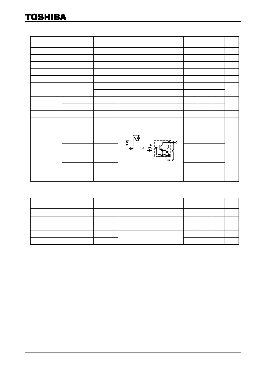
Array Configuration
Industrial Applications
Unit: mm
JEDEC
JEITA
TOSHIBA 2-32B1C
Weight: 6.0 g (typ.)
2
1
R1 R2
6
11
5
R1 4.5 k
8
7
12
R1 R2
4
9
R2 300

MP4503
2002-11-20
2
Thermal Characteristics
Characteristics Symbol
Max
Unit
Thermal resistance of junction to
ambient
(4 devices operation, Ta = 25∞C)
R
th (j-a)
25 ∞C/W
Thermal resistance of junction to case
(4 devices operation, Tc = 25∞C)
R
th (j-c)
5.0 ∞C/W
Maximum lead temperature for
soldering purposes
(3.2 mm from case for 10 s)
T
L
260
∞C
Electrical Characteristics
(Ta = 25∞C)
(NPN transistor)
Characteristics Symbol Test
Condition Min
Typ.
Max
Unit
Collector cut-off current
I
CBO
V
CB
= 100 V, I
E
= 0 A
20 µA
Collector cut-off current
I
CEO
V
CE
= 80 V, I
B
= 0 A
20 µA
Emitter cut-off current
I
EBO
V
EB
= 5 V, I
C
= 0 A
0.5
2.5 mA
Collector-base breakdown voltage
V
(BR) CBO
I
C
= 1 mA, I
E
= 0 A
100
V
Collector-emitter breakdown voltage
V
(BR) CEO
I
C
= 10 mA, I
B
= 0 A
80
V
h
FE (1)
V
CE
= 2 V, I
C
= 1 A
2000
DC current gain
h
FE (2)
V
CE
= 2 V, I
C
= 3 A
1000
Collector-emitter V
CE (sat)
I
C
= 3 A, I
B
= 6 mA
1.5
Saturation voltage
Base-emitter V
BE (sat)
I
C
= 3 A, I
B
= 6 mA
2.0
V
Transition frequency
f
T
V
CE
= 2 V, I
C
= 0.5 A
60 MHz
Collector output capacitance
C
ob
V
CB
= 10 V, I
E
= 0 A, f = 1 MHz
30 pF
Turn-on time
t
on
0.2
Storage time
t
stg
1.5
Switching time
Fall time
t
f
I
B1
= -I
B2
= 6 mA, duty cycle 1%
0.6
µs
Emitter-Collector Diode Ratings and Characteristics
(Ta = 25∞C)
Characteristics Symbol Test
Condition Min
Typ.
Max
Unit
Forward current
I
FM
4 A
Surge current
I
FSM
t = 1 s, 1 shot
6 A
Forward voltage
V
F
I
F
= 1 A, I
B
= 0 A
2.0 V
Reverse recovery time
t
rr
1.0 µs
Reverse recovery charge
Q
rr
I
F
= 4 A, V
BE
= -3 V, dI
F
/dt = -50 A/µs
8 µC
I
B1
20 µs
V
CC
= 30 V
Output
10
I
B2
I
B1
Input
I
B2
MP4503
2002-11-20
3
Electrical Characteristics
(Ta = 25∞C)
(PNP transistor)
Characteristics Symbol Test
Condition Min
Typ.
Max
Unit
Collector cut-off current
I
CBO
V
CB
= -100 V, I
E
= 0 A
-20
µA
Collector cut-off current
I
CEO
V
CE
= -80 V, I
B
= 0 A
-20
µA
Emitter cut-off current
I
EBO
V
EB
= -5 V, I
C
= 0 A
-0.5
-2.5
mA
Collector-base breakdown voltage
V
(BR) CBO
I
C
= -1 mA, I
E
= 0 A
-100
V
Collector-emitter breakdown voltage
V
(BR) CEO
I
C
= -10 mA, I
B
= 0 A
-80
V
h
FE (1)
V
CE
= -2 V, I
C
= -1 A
2000
DC current gain
h
FE (2)
V
CE
= -2 V, I
C
= -3 A
1000
Collector-emitter V
CE (sat)
I
C
= -3 A, I
B
= -6 mA
-1.5
Saturation voltage
Base-emitter V
BE (sat)
I
C
= -3 A, I
B
= -6 mA
-2.0
V
Transition frequency
f
T
V
CE
= -2 V, I
C
= -0.5 A
40 MHz
Collector output capacitance
C
ob
V
CB
= -10 V, I
E
= 0 A, f = 1 MHz
55 pF
Turn-on time
t
on
0.15
Storage time
t
stg
0.80
Switching time
Fall time
t
f
-I
B1
= I
B2
= 6 mA, duty cycle 1%
0.40
µs
Emitter-Collector Diode Ratings and Characteristics
(Ta = 25∞C)
Characteristics Symbol Test
Condition Min
Typ.
Max
Unit
Forward current
I
FM
4 A
Surge current
I
FSM
t = 1 s, 1 shot
6 A
Forward voltage
V
F
I
F
= 1 A, I
B
= 0 A
2.0 V
Reverse recovery time
t
rr
1.0 µs
Reverse recovery charge
Q
rr
I
F
= 4 A, V
BE
= 3 V, dI
F
/dt = -50 A/µs
8 µC
I
B1
V
CC
= -30 V
Output
10
I
B1
I
B2
Input
20 µs
I
B2
MP4503
2002-11-20
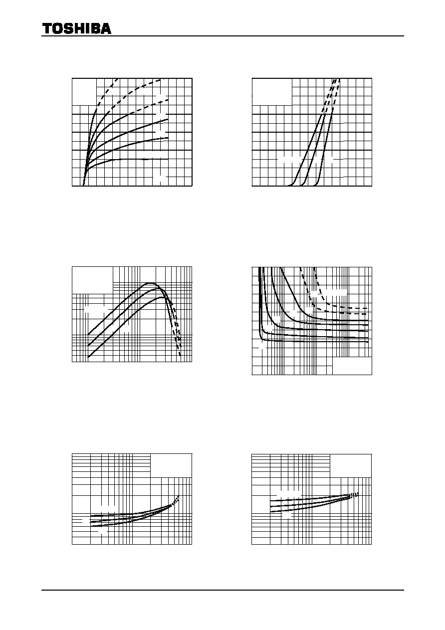
4
Collector current I
C
(A)
h
FE
≠ I
C
D
C
c
u
rr
en
t
g
a
i
n h
FE
Collector-emitter voltage V
CE
(V)
I
C
≠ V
CE
Co
lle
ct
o
r
cu
r
r
e
n
t I
C
(A
)
Base-emitter voltage V
BE
(V)
I
C
≠ V
BE
Co
lle
ct
o
r
cu
r
r
e
n
t I
C
(A
)
Base current I
B
(mA)
V
CE
≠ I
B
Co
lle
ct
o
r
-
e
m
i
tte
r
v
o
lt
a
g
e
V
CE
(V
)
Collector current I
C
(A)
V
BE (sat)
≠ I
C
B
a
se-
e
mi
tte
r sa
tu
rati
on v
o
l
t
age
V
BE (sat)
(V
)
Collector current I
C
(A)
V
CE (sat)
≠ I
C
C
o
l
l
e
ct
or
-e
mi
tte
r s
a
tu
rati
on
vol
t
ag
e
V
CE (sat)
(V
)
300
0.05
0.1 0.3
0.5
1 3
5
10
500
1000
3000
5000
10000
20000
Common emitter
VCE = 2 V
25
Tc = 100∞C
-55
0.3 0.5
1
3 5
10
0.1
10
0.3
0.5
1
3
5
Common emitter
IC/IB = 500
25
Tc = -55∞C
100
0.3 0.5
1
3 5
10
0.1
10
0.3
0.5
1
3
5
Common emitter
IC/IB = 500
25
Tc = -55∞C
100
2
0
0.5
IB = 0.2 mA
0.23
0.3
5
0
1 2 3 4 5 6 7
1
0
6
5
4
3
1
Common
emitter
Tc = 25∞C
Common emitter
VCE = 2 V
0
0
2
0.4 0.8 1.2 1.6 2.0 2.4 2.8
1
6
5
4
3
25
Tc = 100∞C
-55
0
0.1
0.3 1
10 30
100
3 300
2.4
0.4
1.6
2.0
0.8
1.2
0.3
1
2
3
4
5
IC = 6 A
Common emitter
Tc = 25∞C
MP4503
2002-11-20
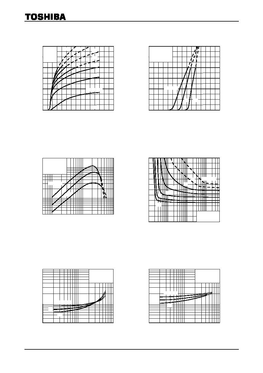
5
Collector-emitter voltage V
CE
(V)
I
C
≠ V
CE
Co
lle
ct
o
r
cu
r
r
e
n
t I
C
(A
)
Base-emitter voltage V
BE
(V)
I
C
≠ V
BE
Co
lle
ct
o
r
cu
r
r
e
n
t I
C
(A
)
Collector current I
C
(A)
h
FE
≠ I
C
D
C
c
u
rr
en
t
g
a
i
n h
FE
Base current I
B
(mA)
V
CE
≠ I
B
Co
lle
ct
o
r
-
e
m
i
tte
r
v
o
lt
a
g
e
V
CE
(V
)
Collector current I
C
(A)
V
BE (sat)
≠ I
C
B
a
se-
e
mi
tte
r sa
tu
rati
on v
o
l
t
age
V
BE (sat)
(V
)
Collector current I
C
(A)
V
CE (sat)
≠ I
C
C
o
l
l
e
ct
or
-e
mi
tte
r s
a
tu
rati
on
vol
t
ag
e
V
CE (sat)
(V
)
300
-0.05
-0.1
-0.3 -0.5
-1
-3
-5
-10
500
1000
3000
5000
10000
20000
Common emitter
VCE = -2 V
25
Tc = 100∞C
-55
0
-0.1
-0.3
-1
-10
-30
-100
-3
-300
-2.4
-0.4
-1.6
-2.0
-0.8
-1.2
Common emitter
Tc = 25∞C
-0.3
-1
-2
-3
-4
-5
IC = -6 A
-0.3 -0.5
-1
-3
-5
-10
-0.1
-10
-0.3
-0.5
-1
-3
-5
Common emitter
IC/IB = 500
25
Tc = -55∞C
100
-0.3 -0.5
-1
-3
-5
-10
-0.1
-0.3
-0.5
-1
-3
-5
Common emitter
IC/IB = 500
25
Tc = -55∞C
100
-2
0
-0.5
IB = -0.2 mA
-0.3
-0.4
-1.0
0
-1
-2
-3
-4
-5
-6
-7
-1
0
-6
-5
-4
-3
-0.7
-1.5
Common
emitter
Tc = 25∞C
Common emitter
VCE = -2 V
0
0
-2
-0.4
-0.8
-1.2
-1.6
-2.0
-2.4
-2.8
-1
-6
-5
-3
25
Tc = 100∞C
-55
-4