MT6L58AE
2003-07-31
1
TOSHIBA Transistor Silicon NPN Epitaxial Planar Type
MT6L58AE
VHF~UHF Band Low Noise Amplifier Applications
∑ Two devices are built in to the super-thin and extreme super mini (6
pins) package: ES6
Mounted Devices
Q1: SSM (TESM)
Q2: SSM (TESM)
Three-pins (SSM/TESM) mold
products are corresponded.
MT3S06S
(MT3S06T)
MT3S03AS
(MT3S03AT)
Maximum Ratings
(Ta
=
=
=
=
25∞C)
Characteristics Symbol
Q1
Q2
Unit
Collector-base voltage
V
CBO
10 10 V
Collector-emitter voltage
V
CEO
5 5 V
Emitter-base voltage
V
EBO
1.5 2 V
Collector current
I
C
15
40
mA
Base current
I
B
7
10
mA
Collector power dissipation
P
C
(Note 1)
100 mW
Junction temperature
T
j
125 ∞C
Storage temperature range
T
stg
-55~125 ∞C
Note 1: Total power dissipation of Q1 and Q2.
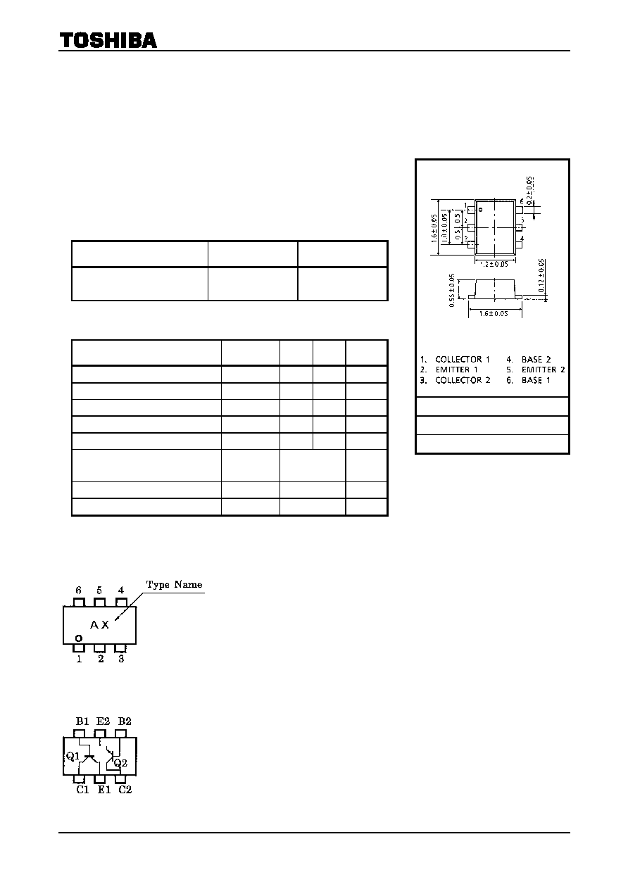
Marking
Pin Assignment
(top view)
Unit: mm
JEDEC
JEITA
TOSHIBA 2-2N1C
Weight: 0.003 g (typ.)

MT6L58AE
2003-07-31
2
Electrical Characteristics Q1
(Ta
=
=
=
=
25∞C)
Characteristics Symbol Test
Condition Min
Typ.
Max
Unit
Collector cut-off current
I
CBO
V
CB
= 5 V, I
E
= 0
0.1 µA
Emitter cut-off current
I
EBO
V
EB
= 1 V, I
C
= 0
1 µA
DC current gain
h
FE
V
CE
= 1 V, I
C
= 5 mA
70
140
Transition frequency
f
T
V
CE
= 3 V, I
C
= 5 mA
7
10
GHz
S
21e
2
(1)
V
CE
= 1 V, I
C
= 5 mA, f = 2 GHz
7.5
Insertion gain
S
21e
2
(2)
V
CE
= 3 V, I
C
= 7 mA, f = 2 GHz
4.5
8
dB
NF (1)
V
CE
= 1 V, I
C
= 3 mA, f = 2 GHz
1.7 3
Noise figure
NF (2)
V
CE
= 3 V, I
C
= 3 mA, f = 2 GHz
1.6 3
dB
Reverse transfer capacitance
C
re
V
CB
= 1 V, I
E
= 0, f = 1 MHz
(Note 2)
0.35 0.75 pF
Note 2: C
re
is measured by 3 terminal method with capacitance bridge.
Electrical Characteristics Q2
(Ta
=
=
=
=
25∞C)
Characteristics Symbol Test
Condition Min
Typ.
Max
Unit
Collector cut-off current
I
CBO
V
CB
= 5 V, I
E
= 0
0.1 µA
Emitter cut-off current
I
EBO
V
EB
= 1 V, I
C
= 0
1 µA
DC current gain
h
FE
V
CE
= 1 V, I
C
= 5 mA
80
160
f
T
(1)
V
CE
= 1 V, I
C
= 5 mA
5
7
Transition frequency
f
T
(2)
V
CE
= 3 V, I
C
= 10 mA
7
10
GHz
S
21e
2
(1)
V
CE
= 1 V, I
C
= 5 mA, f = 2 GHz
5
Insertion gain
S
21e
2
(2)
V
CE
= 3 V, I
C
= 20 mA, f = 2 GHz
3
6.5
dB
NF (1)
V
CE
= 1 V, I
C
= 5 mA, f = 2 GHz
1.7 3
Noise figure
NF (2)
V
CE
= 3 V, I
C
= 7 mA, f = 2 GHz
1.4 2.2
dB
Reverse transfer capacitance
C
re
V
CB
= 1 V, I
E
= 0, f = 1 MHz
(Note 2)
0.8 1.15 pF
Note 2: C
re
is measured by 3 terminal method with capacitance bridge.
Handling Precaution
When handling individual devices (which are not yet mounted on a circuit board), be sure that the environment
is protected against electrostatic electricity. Operators should wear anti-static clothing, and containers and other
objects that come into direct contact with devices should be made of anti-static materials.

MT6L58AE
2003-07-31
3
∑ The information contained herein is subject to change without notice.
∑ The information contained herein is presented only as a guide for the applications of our products. No
responsibility is assumed by TOSHIBA for any infringements of patents or other rights of the third parties which
may result from its use. No license is granted by implication or otherwise under any patent or patent rights of
TOSHIBA or others.
∑ TOSHIBA is continually working to improve the quality and reliability of its products. Nevertheless, semiconductor
devices in general can malfunction or fail due to their inherent electrical sensitivity and vulnerability to physical
stress. It is the responsibility of the buyer, when utilizing TOSHIBA products, to comply with the standards of
safety in making a safe design for the entire system, and to avoid situations in which a malfunction or failure of
such TOSHIBA products could cause loss of human life, bodily injury or damage to property.
In developing your designs, please ensure that TOSHIBA products are used within specified operating ranges as
set forth in the most recent TOSHIBA products specifications. Also, please keep in mind the precautions and
conditions set forth in the "Handling Guide for Semiconductor Devices," or "TOSHIBA Semiconductor Reliability
Handbook" etc..
∑ The TOSHIBA products listed in this document are intended for usage in general electronics applications
(computer, personal equipment, office equipment, measuring equipment, industrial robotics, domestic appliances,
etc.). These TOSHIBA products are neither intended nor warranted for usage in equipment that requires
extraordinarily high quality and/or reliability or a malfunction or failure of which may cause loss of human life or
bodily injury ("Unintended Usage"). Unintended Usage include atomic energy control instruments, airplane or
spaceship instruments, transportation instruments, traffic signal instruments, combustion control instruments,
medical instruments, all types of safety devices, etc.. Unintended Usage of TOSHIBA products listed in this
document shall be made at the customer's own risk.
∑ TOSHIBA products should not be embedded to the downstream products which are prohibited to be produced
and sold, under any law and regulations.
030619EAA
RESTRICTIONS ON PRODUCT USE