RN2501~RN2506
2001-06-07
1
TOSHIBA Transistor Silicon PNP Epitaxial Type (PCT Process)
RN2501,RN2502,RN2503
RN2504,RN2505,RN2506
Switching, Inverter Circuit, Interface Circuit
And Driver Circuit Applications
l Including two devices in SMV (super mini type with 5 leads)
l With built-in bias resistors
l Simplify circuit design
l Reduce a quantity of parts and manufacturing process
l Complementary to RN1501~RN1506
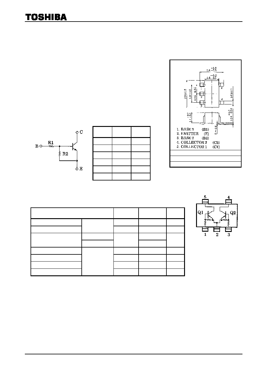
Equivalent Circuit and Bias Resistor Values
Equivalent Circuit
(Top View)
Maximum Ratings
(Ta = 25
∞
∞
∞
∞
C) (Q1, Q2 Common)
Characteristic Symbol
Rating
Unit
Collector-base voltage
V
CBO
-50 V
Collector-emitter voltage
RN2501~2506
V
CEO
-50 V
RN2501~2504
-10
Emitter base voltage
RN2505, 2506
V
EBO
-5
V
Collector current
I
C
-100 mA
Collector power dissipation
P
C
* 300
mW
Junction temperature
Tj
150
∞C
Storage temperature range
RN2501~2506
Tstg
-55~150
∞C
* Total
rating
JEDEC
EIAJ
TOSHIBA 2-3L1A
Weight: 0.014g
Type No.
R1 (k)
R2 (k)
RN2501 4.7 4.7
RN2502 10
10
RN2503 22
22
RN2504 47
47
RN2505 2.2
47
RN2506 4.7
47
Unit: mm
RN2501~RN2506
2001-06-07
2
Electrical Characteristics
(Ta = 25
∞
∞
∞
∞
C) (Q1, Q2 Common)
Characteristic Symbol
Test
Circuit
Test Condition
Min
Typ.
Max
Unit
I
CBO
V
CB
= -50V, I
E
= 0
-100
Collector cut-off current RN2501~2506
I
CEO
V
CE
= -50V, I
B
= 0
-500
nA
RN2501
-0.82
-1.52
RN2502
-0.38
-0.71
RN2503
-0.17
-0.33
RN2504
V
EB
= -10V, I
C
= 0
-0.082
-0.15
RN2505
-0.078
-0.145
Emitter cut-off current
RN2506
I
EBO
V
EB
= -5V, I
C
= 0
-0.074
-0.138
mA
RN2501
30
RN2502
50
RN2503
70
RN2504
80
RN2505
80
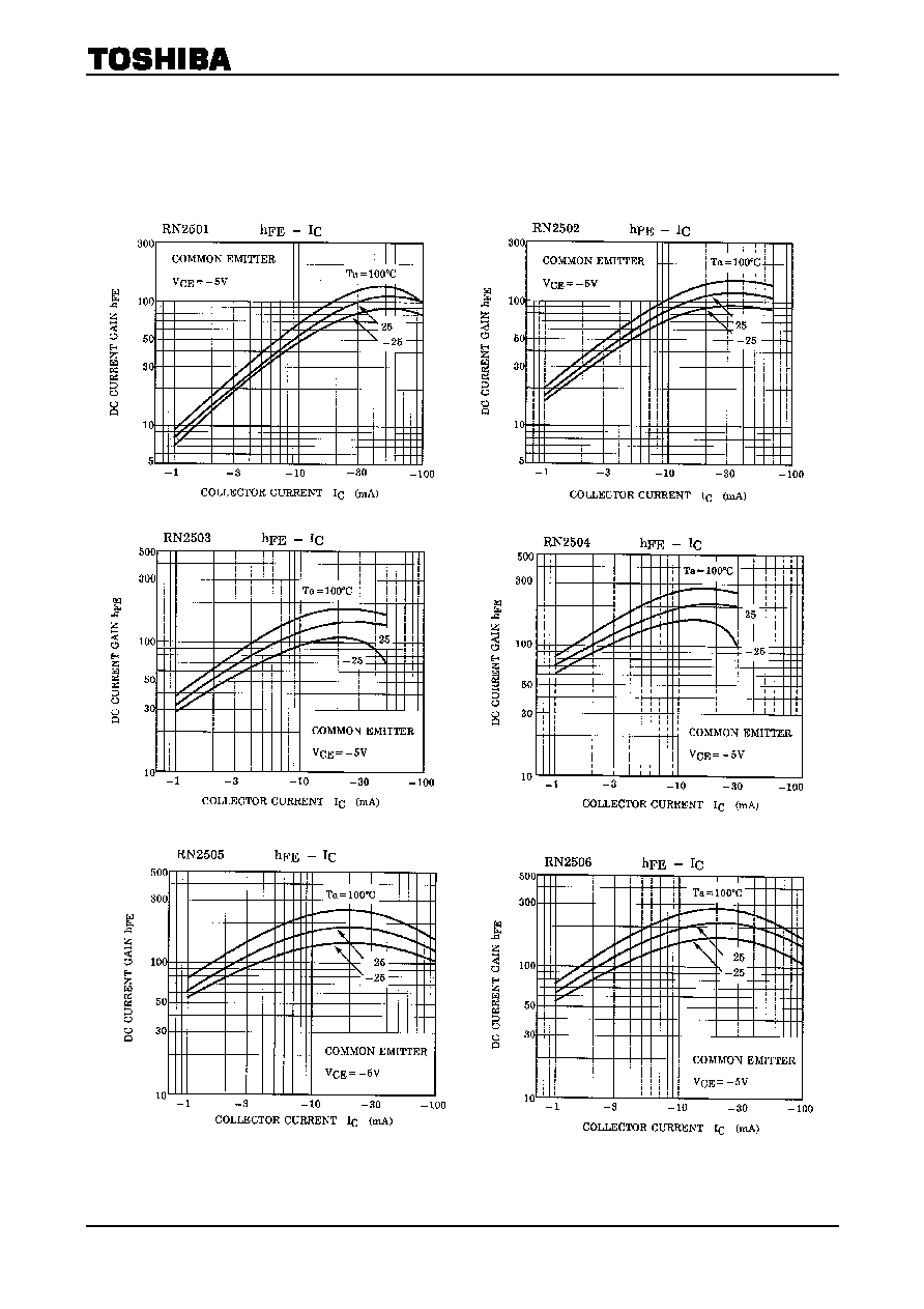
DC current gain
RN2506
h
FE
V
CE
= -5V
I
C
= -10mA
80
Collector-emitter
saturation voltage
RN2501~2506 V
CE (sat)
I
C
= -5mA
I
B
= -0.25mA
-0.1
-0.3
V
RN2501
-1.1
-2.0
RN2502
-1.2
-2.4
RN2503
-1.3
-3.0
RN2504
-1.5
-5.0
RN2505
-0.6
-1.1
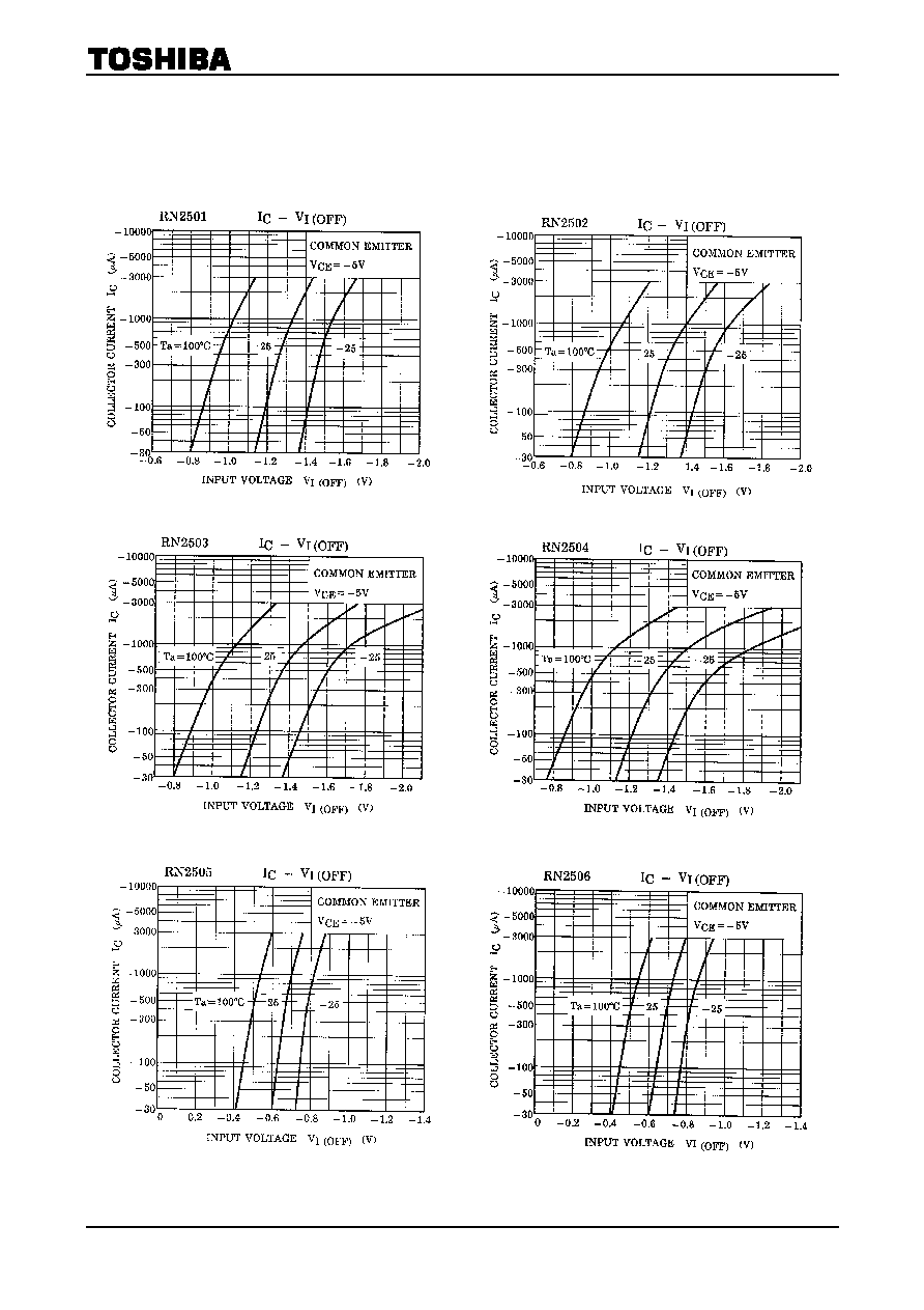
Input voltage (ON)
RN2506
V
I (ON)
V
CE
= -0.2V
I
C
= -5mA
-0.7
-1.3
V
RN2501~2504
-1.0
-1.5
Input voltage (OFF)
RN2505, 2506
V
I (OFF)
V
CE
= -5V
I
C
= -0.1mA
-0.5
-0.8
V
Translation frequency
RN2501~2506
f
T
V
CE
= -10V
I
C
= -5mA
200 MHz
Collector output
capacitance
RN2501~2506 C
ob
V
CB
= -10V, I
E
= 0
f = 1MHz
3 6 pF
RN2501
3.29
4.7
6.11
RN2502
7
10
13
RN2503
15.4 22 28.6
RN2504
32.9 47 61.1
RN2505
1.54
2.2
2.86
Input resistor
RN2506
R1
3.29 4.7 6.11
k
RN2501~2504
0.9 1.0 1.1
RN2505
0.0421 0.0468 0.0515
Resistor ratio
RN2506
R1/R2
0.09 0.1 0.11