S-AV10L,S-AV10H
2003-03-27
1
TOSHIBA RF Power Amplifier Module
S-AV10L,S-AV10H
VHF RF Power Amplifier Module
∑ High gain: Po 14 W, G
p
1.85dB,
T
40%
∑ S-AV10L 135~155 MHz
∑ S-AV10H 150~175 MHz
Maximum Ratings
(Tc
=
=
=
=
25∞C)
Characteristics Symbol
Rating
Unit
DC supply voltage
V
CC
16 V
DC supply voltage
V
CON
16 V
Input power
Pi
300
mW
Operating case temperature range
T
c (opr)
-30~100 ∞C
Storage temperature range
T
stg
-40~110 ∞C
Electrical Characteristics
(Tc
=
=
=
=
25∞C)
Characteristics Symbol Test
Condition Min
Typ.
Max
Unit
Frequency range
f
range
æ 135
æ 175
MHz
Output power
Po
14
æ
æ W
Power gain
G
P
18.5
æ
æ dB
Total efficiency
h
T
40
æ
æ %
Input VSWR
VSWR
in
æ
æ 2 æ
Harmonics HRM
Pi
= 200 mW
V
CC
= 12.5 V, V
CON
= 12.5 V
Z
G
= Z
L
= 50 W
æ
æ
-25
dB
Load mismatch
æ
V
CC
= 15 V, V
CON
= 12.5 V
Po
= 15 W (Pi = adjust)
VSWR load 20: 1 all phase
No degradation
æ
Power slump
æ
Tc
= -30~80∞C
V
CC
= 12.5 V, Pi = 200 mW
Po
= 14 W (@Tc = 25∞C)
æ 0.8 æ dB
Stability
æ
V
CC
= 12.5 V, Pi = 200 mW
V
CON
= 0~12.5 V
VSWR Load 3: 1 all phase
All spurious output than
60dB below desired
signal
æ
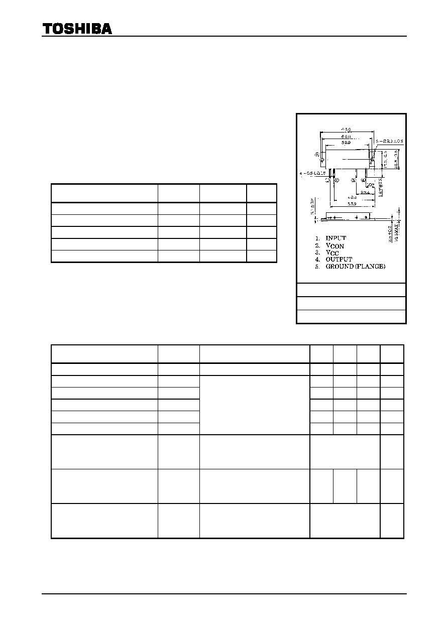
Unit: mm
JEDEC
JEITA
TOSHIBA 5-53P
Weight: 35 g (typ.)
S-AV10L,S-AV10H
2003-03-27
2
Caution
This product has intersetting cap. Please pay attention for exceeding stress and foreign matter in your
application. And not to take away the cap.
Beryllia Ceramics is used in this product. The dust or vapor can be dangerous to humans. Do not break, cut,
crush or dissolve chemically. Dispose of this product properly according to law. Do not intermingle with normal
industrial or domestic waste.
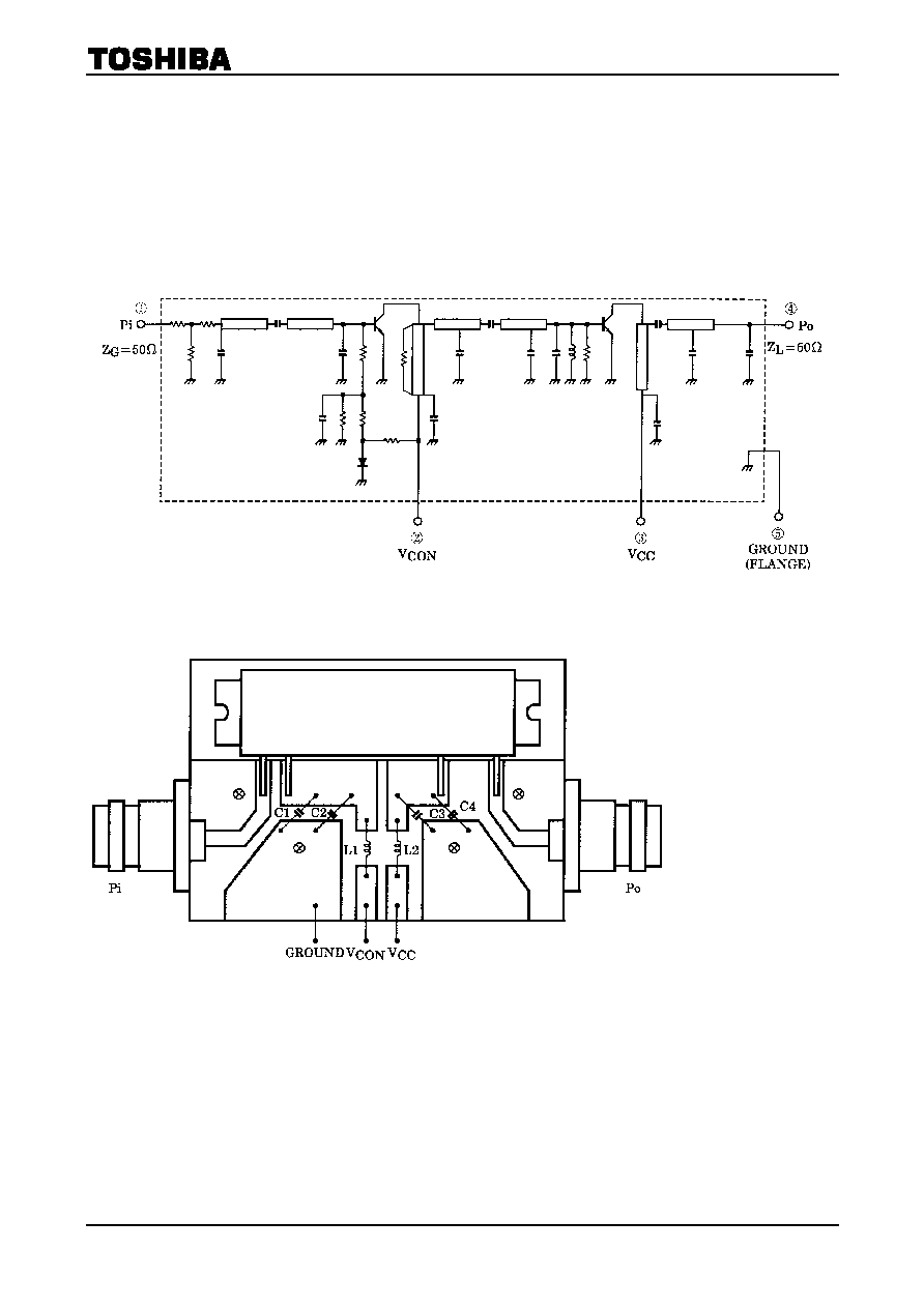
Schematic
Test Fixture
C1, C3: 15000 pF
C2, C4: 10
mF
L1, L2:
f0.8 enamel wire, 8 T, 5ID
S-AV10L,S-AV10H
2003-03-27
4
∑ TOSHIBA is continually working to improve the quality and reliability of its products. Nevertheless, semiconductor
devices in general can malfunction or fail due to their inherent electrical sensitivity and vulnerability to physical
stress. It is the responsibility of the buyer, when utilizing TOSHIBA products, to comply with the standards of
safety in making a safe design for the entire system, and to avoid situations in which a malfunction or failure of
such TOSHIBA products could cause loss of human life, bodily injury or damage to property.
In developing your designs, please ensure that TOSHIBA products are used within specified operating ranges as
set forth in the most recent TOSHIBA products specifications. Also, please keep in mind the precautions and
conditions set forth in the "Handling Guide for Semiconductor Devices," or "TOSHIBA Semiconductor Reliability
Handbook" etc..
∑ The TOSHIBA products listed in this document are intended for usage in general electronics applications
(computer, personal equipment, office equipment, measuring equipment, industrial robotics, domestic appliances,
etc.). These TOSHIBA products are neither intended nor warranted for usage in equipment that requires
extraordinarily high quality and/or reliability or a malfunction or failure of which may cause loss of human life or
bodily injury ("Unintended Usage"). Unintended Usage include atomic energy control instruments, airplane or
spaceship instruments, transportation instruments, traffic signal instruments, combustion control instruments,
medical instruments, all types of safety devices, etc.. Unintended Usage of TOSHIBA products listed in this
document shall be made at the customer's own risk.
∑ The information contained herein is presented only as a guide for the applications of our products. No
responsibility is assumed by TOSHIBA CORPORATION for any infringements of intellectual property or other
rights of the third parties which may result from its use. No license is granted by implication or otherwise under
any intellectual property or other rights of TOSHIBA CORPORATION or others.
∑ The information contained herein is subject to change without notice.
000707EAA
RESTRICTIONS ON PRODUCT USE
