 | –≠–ª–µ–∫—Ç—Ä–æ–Ω–Ω—ã–π –∫–æ–º–ø–æ–Ω–µ–Ω—Ç: T6A04A | –°–∫–∞—á–∞—Ç—å:  PDF PDF  ZIP ZIP |

T6A04A
2002-03-06
1
TOSHIBA CMOS Digital Integrated Circuit Silicon Monolithic
T6A04A
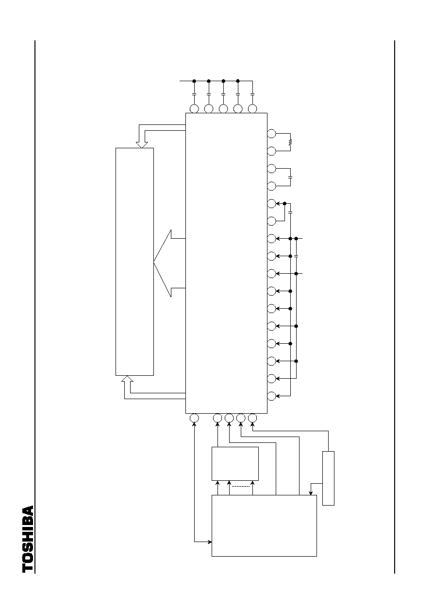
Column and Row Driver LSI for a Dot Matrix Graphic LCD
The T6A04A is a driver for a small-to-medium-sized scale dot
matrix graphic LCD. It includes the functions of the T9841B
(column driver) and the T9842B (row driver). It has an 8-bit
interface circuit and can be operated with an 80-Series MPU. It
generates all the timing signals for the display with an on-chip
oscillator. It receives 8-bit data from an MPU, latches the data to
an on-chip RAM, and displays the image on the LCD (the data in
the display RAM correspond to the dots on the display). The
device has 120 column driver outputs and 64 row driver outputs
enabling it to drive a 120-dot by 64-dot LCD. In addition, there
are resistors to divide the bias voltage, a power supply op-amp,
DC-DC converter (+5 V -5 V) and contrast control circuit,
enabling the LCD to be driven by a single power supply. The
device can be connected to another T6A04A to drive a 240-dot by
64-dot LCD.
Features
∑ On-chip display RAM capacity
: 120 ◊ 64 = 7.5 kbits
∑ Display RAM data
(1) Display data = 1.................. LCD turns on.
(2) Display data = 0.................. LCD turns off.
∑ 1/64 duty cycle
∑ Word length of display data can be switched between eight bits and six bits according to the character font.
∑ LCD driver outputs
: 120 column driver outputs and 64 row driver outputs
∑ Interface with 80-series MPU
∑ On-chip oscillator with one external resistor
∑ Low power consumption
∑ On-chip resistors to divide bias voltage, on-chip operational amplifier for LCD supply, on-chip DC-DC converter,
on-chip contrast control circuit
∑ CMOS process
∑ Operating voltage
: 4.5 to 5.5 V
∑ Operating voltage for LCD drive signal : V
DD
- V
EE
= 16.0 V (max)
∑ Package
: TCP (tape carrier package)
Unit: mm
Lead Pitch
IN
T6A04A
(UAW, 6NS)
OUT
(UEM, 7NS)
1.0
0.4
0.28
0.4
Please contact Toshiba or an authorized
Toshiba dealer for information on package
dimensions.
TCP (Tape Carrier Package)

T6A04A
200
2-
03-
0
6
2
B
l
ock D
i
agr
a
m
COM
1
LCD DRI
V
E CI
RCUI
T
(32)
32-bi
t
S
H
I
F
T
RE
G
I
S
T
E
R
LCD
DRI
V
E
CI
RCUI
T
(32)
32-bi
t
S
H
I
F
T
RE
G
I
S
T
E
R
LCD DRI
V
E
CI
RCUI
T
(120)
LA
TCH
IN
PU
T/
OU
TPU
T
GA
TE
Y-
AD
D
R
E
S
S
COUNT
E
R/
DE
COD
E
R
MP
X
X-COUNT
E
R
Z
-
COUNT
E
R
TIM
I
N
G
GE
NE
RAT
I
ON
CI
RCUI
T
OS
CI
LLA
TOR
OP
-A
M
P
(
¥
5)
R
E
SI
STO
R
L
A
D
D
ER
S
CONT
RA
S
T
CONT
ROL
CI
RCUI
T
DC-DC
CONV
E
R
T
E
R
IN
PU
T/
OU
TPU
T
BU
FFER
OU
TPU
T
BU
FF
ER
IN
PU
T/
OU
TPU
T
BU
FFER
I
/
F
CONT
ROL
CI
RCUI
T
IN
PU
T/
OU
TPU
T
BU
F
F
ER
OUTP
UT
RE
GIS
T
E
R
IN
PU
T
RE
GIS
T
E
R
WO
R
D
LE
NGTH
CONV
E
R
T
E
R
RE
GIS
T
E
R
Z-
AD
D
R
ES
S
RE
GIS
T
E
R
COUNT
E
R
UP
/
D
O
W
N
R
E
G
I
STER
X
Y C
O
U
N
TER
SEL
EC
T
R
E
G
I
STER
DI
S
P
L
A
Y
ON
/OFF
RE
GIS
T
E
R
CONT
RA
S
T
CONT
ROL
R
E
G
I
STER
OP
-A
M
P
CONT
ROL
RE
GIS
T
E
R
BIT
TR
AN
SF
ER
CI
RCUI
T
COM
32 COM
3
3
C
OM
64
S
E
G1
S
E
G
120
MP
X
M/
S
FS1 FS2
V
LC
1
R
1
C
1
C
2
COM
D
S
C
LK
OS
C1
OS
C2
/
f
PM
C
L
FR
M
M
/ST
B
EX
P
/R
ST
D
/
I
/
W
R
/C
E
D
B0
to
D
B
7
8
8
84
4
8
5
3
2
3
V
LC
2
V
LC
3
V
LC
4
V
LC
5
R
2
V
EE
V
IN
V
OUT
DECODE
R
120
DI
S
P
L
A
Y RA
M
120
¥
64
=
7
.
5
kb
i
t
s

T6A04A
2002-03-06
3
Pin Assignment
Note 1: The above diagram shows the pin configuration of the LSI chip; it does not show the configuration of the
tape carrier package.
T6A04A
(top view)
DB0
DB1
DB2
DB3
DB4
DB5
DB6
DB7
/RST
/CE
/WR
D/I
EXP
M/S
OSC2
OSC1
FS2
FS1
V
DD
/
f
PM
fB
fA
P
f
FRM
M
C
L
COMB
V
SS
/STB
V
OUT
C
2
C
1
V
IN
R
2
R
1
V
EE
V
LC1
V
LC2
V
LC3
V
LC4
V
LC5
COM32
COM1
SEG1
SEG120
COM33
COM64

T6A04A
2002-03-06
4
Pin Functions
Pin Name
I/O
Functions
SEG1 to SEG120
Output
Column driver output
COM1 to COM64
Output
Row driver output
Disable
expansion
mode
(EXP
= L, M/S = H)
Æ COM1 to COM64 are enabled.
Enable expansion mode/master mode (EXP
= H, M/S = H)
Æ COM1 to COM32 are enabled and COM33 to COM64 are disabled.
Enable expansion mode/slave mode (EXP
= H, M/S = L)
Æ COM1 to COM32 are disabled and COM33 to COM64 are enabled.
CL
I/O
Input/output for shift clock pulse
Master
mode
(M/S
= H) Æ Output
Slave
mode
(M/S
= L) Æ Input
M I/O
Input/output for frame signal
Master
mode
(M/S
= H) Æ Output
Slave
mode
(M/S
= L) Æ Input
FRM I/O
Input/output for display synchronous signal
Master
mode
(M/S
= H) Æ Output
Slave
mode
(M/S
= L) Æ Input
P
f, fA, fB I/O
Input/output system clock signal
Master
mode
(M/S
= H) Æ Output
Slave
mode
(M/S
= L) Æ Input
COMD I/O
Input/output row signal data
Master
mode
(M/S
= H) Æ Output
Slave
mode
(M/S
= L) Æ Input
DB0 to DB7
I/O
Data bus
D/I Input
Input for data/instruction select signal
D/I
= H Æ indicates that the data on DB0 to DB7 is display data.
D/I
= L Æ indicates that the data on DB0 to DB7 is control data.
/WR Input
Input for write select signal
/WR
= H Æ Read selected
/WR
= L Æ Write selected
/CE Input
Input for chip enable signal
/WR
= L Æ Data on DB0 to DB7 is latched on the rising edge of /CE.
/WR
= H Æ Data appears at DB0 to DB7 while /CE is Low.
/RST Input
Input for reset signal
/RST
= L Æ Reset state
/STB Input
Input for standby signal
Usually
connected
to
V
DD
/STB
= L Æ T6A04A is in standby state and cannot accept any commands or data.
Column driver signal and row driver signal are at the V
DD
level
FS1, FS2
Input
Input for frequency selection
EXP Input
Input for expansion mode selection
M/S
= H Æ enables expansion mode. Two chips can be used together.
M/S
= L Æ disables expansion mode.

T6A04A
2002-03-06
5
Pin Name
I/O
Functions
M/S Input
Input for master/slave selection
M/S
= H Æ T6A04A is master chip.
M/S
= L Æ T6A04A is slave chip.
OSC1, OSC2
æ
When using the internal clock oscillator, connect a resistor between OSC1 and OSC2.
When using an external clock, connect the clock as input to OSC1 and leave OSC2 open.
R1, R2
æ
Input for LCD drive bias selection
LCD drive bias selection is shown in the following
table
R
2
R
1
Bias
0 0
1/6
0 1
1/7
1 0
1/8
1 1
1/9
C1, C2
æ
Connected by a capacitor for DC-DC converter
VIN
æ
Input for DC-DC converter. Connect to V
DD
.
VOUT
æ
DC-DC converter output
VEE
æ
Power supply for LCD driver circuit
When using on-chip DC-DC converter, connect VEE to VOUT
VLC1 to VLC5
æ
Power supply for LCD driver circuit
M/S
= H Æ bias voltage output
M/S
= L Æ bias voltage input
V
DD
æ
Power supply for logic circuit
VSS
æ Ground:
Reference
PM
æ
Pre-frame signal for Toshiba T9841B
/
f
æ
Output system clock for Toshiba T9841B

T6A04A
2002-03-06
6
Function of Each Block
∑ Interface logic
The T6A04A can be operated with an 80-Series MPU.
Figure 1 shows an example of the interface.
∑ Input register
This register stores 8-bit data from the MPU. The D/I signal distinguishes between command data and
display data.
∑ Output register
This register stores 8-bit data from the display RAM. When display data is read, the display data specified by
the address in the address counter is stored in this register. After that, the address is automatically
incremented or decremented. Therefore, when an address is set, the correct data does not appear as the first
data item that is read. The data in the specified address location appears as the second data item that is read.
∑ X-address counter
The X-address counter is a 64-up/down counter. It holds the row address of a location in the display RAM.
Writing data to or reading data from the display RAM causes the X-address to be automatically incremented
or decremented.
∑ Y-(page) address counter
The Y-(page) address counter is either a 15-up/down counter, when the word length is eight bits, or a
20-up/down counter, when the word length is six bits. It holds the column address of a location in the display
RAM. Writing data to or reading data from the display RAM causes the Y-address to be automatically
incremented or decremented.
∑ Z-address counter
The Z-address counter is a 64-up counter that provides the display RAM data for the LCD drive circuit. The
data stored in the Z-address register is sent to the Z-address counter as the Z start address.
For instance, when the Z start address is 32, the counter increments as follows: 32, 33, 34 ..., 62, 63, 0, 1, 2 ...
30, 31, 32. Therefore, the display start line is line 32 of the display RAM.
∑ Up/down register
The 1-bit datum stored in this register selects either Up or Down mode for the X-and Y-(page) address
counters.
∑ Counter select register
The 1-bit datum stored in this register selects the X-address counter or Y-(page) address counter.
∑ Display ON/OFF register
This 1-bit register holds the display ON/OFF state. In the OFF state, the output data from the display RAM is
cleared. In the ON state, the display RAM data is displayed. The display ON/OFF state does not affect the data
in the display RAM.
∑ Z-address register
This 6-bit register holds the data which specifies the display start line. The data is loaded into the Z-address
counter on the FRM signal. Using the Z-address register, vertical scrolling is possible.
A0
/IORQ
/WR
<MPU>
D0 to D7
/RESET
D/1
/CE
/WR
<T6A04A>
DB0 to DB7
/RST
Figure 1

T6A04A
2002-03-06
7
∑ Word length register
The 1-bit datum stored in this register selects the word length: eight bits per word or six bits per word.
∑ Word length change circuit
This circuit is controlled by the word length register. when the word length is eight bits, data is transferred
eight bits at a time. When the word length is six bits, the data transfer method is shown in Figure 2 as follows:
∑ Oscillator
The T6A04A includes an on-chip oscillator. When using this oscillator, connect an external resistor between
OSC1 and OSC2, as shown in Figure 3. When using an external clock, connect the clock input to OSC1 and
leave OSC2 open.
∑ Timing generation circuit
This circuit divides the signals from the oscillator and generates the display timing signals and the operating
clock signal.
∑ Shift register
The T6A04A has two 32-bit shift registers. In disable expansion mode, both the shift registers are enabled.
These two 32-bit shift registers can be combined to form a 64-bit shift register. In enable expansion mode the
32-bit shift register for COM1 to COM32 is enabled in master chip mode, and the 32-bit shift register for
COM33 to COM64 is enabled in slave chip mode.
∑ Latch circuit
The latch circuit latches data from the display RAM on the rising edge of the C
L
signal.
D
4
D
5
*
*
D
3
D
2
D
1
D
0
D
4
D
5
*
*
D
3
D
2
D
1
D
0
Word length
change circuit
Word length
change circuit
D
4
D
5
D
6
D
7
D
3
D
2
D
1
D
0
D
4
D
5
0
0
D
3
D
2
D
1
D
0
*: INVALID
DB0
DB1
DB2
DB3
DB4
DB5
DB6
DB7
DB0
DB1
DB2
DB3
DB4
DB5
DB6
DB7
Display
RAM
MPU
Figure 2
OSC1 OSC2
Internal Circuit
/STB
Figure 3

T6A04A
2002-03-06
8
∑ Column driver circuit
The column driver circuit consists of 120 driver circuits. One of the four LCD driving levels is selected by the
combination of the M signal and the display data transferred from the latch circuit. Details of the column driver
circuit are shown in Figure 4.
∑ Row driver circuit
The row driver circuit consists of 64 driver circuits. One of the four LCD driving levels is selected by the
combination of the M signal and the data from the shift-register. Details of the row driver circuit are shown in
Figure 5.
Figure 4
V
LC5
SEG1 to SEG120
V
LC3
V
DD
V
LC2
M
Vcon
Vcoff
Display Data
Figure 5
V
DD
COM1 to COM64
V
LC4
V
LC5
V
LC1
M
Vron
Vroff
Shift Data

T6A04A
2002-03-06
9
∑ DC-DC converter
The T6A04A has an on-chip DC-DC converter. When +5 V is applied to V
IN
, the DC-DC converter generates
-5 V at V
OUT
. The voltage from V
OUT
will drop due to the load current for V
EE
.
This characteristic is defined in "Electrical Characteristics".
Normally the value of external capacitors is 1.0 mF; this value may need some adjustment according to the
application. When the T6A04A is in standby state, V
OUT
= 0 V. See Figure 6.
When using an external power supply, input the voltage to V
EE
and leave the C
1
, C
2
V
OUT
pins open.
External capacitor C
= 1.0 mF
External capacitor C
= 1.0 mF
Usually connected to V
DD
Usually connected to V
EE
V
OUT
V
IN
C
1
C
2
DC-DC
Figure 6

T6A04A
2002-03-06
10
∑ Voltage divider resistors, contrast control circuit
The T6A04A has on-chip resistors which include op-amps, that divide the bias voltage, and a contrast control
circuit. The voltage bias is modified by the values of R
1
and R
2
. One of four biases can be selected. These
resistors and the contrast control circuit are shown in Figure 7 below.
∑ Op-amp, op-amp control register
The T6A04A has five operational amplifiers which determine the LCD driving level. The power supplied by
these op-amps is modified by the contents of the op-amp control register to match the LCD panel. The op-amp
can also be controlled in such a way that it supplies full current on the rising edge of C
L
and a reduced current
otherwise.
To maintain good LCD contrast, connect a capacitor between the op-amp output and V
DD
. The value of the
capacitor should normally be in the range 0.1 to 1.0 mF.
Figure 7
/STB
5RB
4RB
3RB
2RB
R
2
R
1
RB
RB
V
DD
V
LC1
RB
RB
V
LC3
V
LC4
V
LC5
DB0
RC
DB1
2RC
DB2
4RC
DB3
8RC
DB4
16RC
DB5
32RC
V
EE
DB6
DB7
Cont
ras
t
Cont
rol
Regi
s
t
er
=
Voltage Follower Circuit
R
B
= 134 kW (typ.)
R
C
= 10.1 kW (typ.)
Decoder
V
LC2
Decoder

T6A04A
2002-03-06
11
∑ Display RAM
The display RAM consists of 64 rows ¥ 120 columns for a total of 7680 cells. It is directly bit-mapped to the
LCD. The relation between the display RAM and LCD is shown in Figure 8.
When the word length is set to eight bits, the display RAM is arranged in 15 pages and each page contains 64
words. When the word length is set to six bits, the display RAM is arranged in 20 pages and each page contains
64 words. See Figure 8.
(1) 8-bits-per-word
mode
(2) 6-bits-per-word
mode
Figure 8
D
1
D
3
D
2
D
0
D
7
D
6
D
5
D
4
D
3
D
2
D
1
D
0
D
6
D
5
D
4
1
SEG
1
0
D
7
0
SEG
2
1
1
SEG
3
0
0
SEG
4
1
1
SEG
5
0
0
SEG
6
1
1
SEG
7
0
0
SEG
8
1
1
SEG
9
0
0
SEG
1
0
1
1
SEG
1
1
0
0
SEG
1
2
1
1
SEG
1
3
0
0
SEG
1
4
1
1
SEG
1
5
0
0
SEG
1
6
1
S
E
G
120
COM1
COM2
COM64
120
¥ 64 dot LCD
XAD0
XAD1
XAD63
120
¥ 64 bit DISPLAY RAM
MS
B
L
SB
X
-
A
ddress
D
7
D
0
PAGE13
PAGE14
PAGE1
PAGE2
PAGE0
Y- (page) Address
X-Address
XAD0
XAD1
XAD62
XAD63
D
5
D
0
PAGE18 PAGE19
PAGE1
PAGE2
PAGE0
Y- (page) Address
X-Address
XAD0
XAD1
XAD62
XAD63
Figure 9

T6A04A
2002-03-06
12
Command Definitions
Command
Name
D/I /WR DB7 DB6 DB5
DB4
DB3
DB2
DB1
DB0
Function
DPE
0 0 0 0 0 0 0 0 1 1/0
Display
ON
(1)/OFF
(0)
86E
0
0
0
0
0
0
0
0
0
1/0
Word Length: 8 bits (1)/6 bits (0)
UDE
0 0 0 0 0 0 0 1 1/0
1/0
Counter Select : DB1 Y (1)/X (0)
Mode Select
: DB0 UP (1)/DOWN (0)
CHE
0 0 0 0 0 1 1 * * *
Test Mode Select
OPA1
0 0 0 0 0 1 0 *
1/0
1/0
Op-amp Power Control 1
OPA2
0 0 0 0 0 0 1 *
1/0
1/0
Op-amp Power Control 2
SYE
0
0
0
0
1
Y-(page) Address (0 to 19)
Y-(page) Address Set
SZE
0
0
0
1
Z-Address (0 to 63)
Z-Address Set
SXE
0
0
1
0
X-Address (0 to 63)
X-Address Set
SCE
0
0
1
1
CONTRAST CONTROL (0 to 63)
Contrast Set
STRD 0
1
B
8/6
D
R
0
0
Y/X
U/D Status
Read
DAWR
1
0
Write Data
Display Data Write
DARD
1
1
Read Data
Display Data Read
*: INVALID
∑ Display ON/OFF select (DPE)
/WR D/I DB7 DB6 DB5 DB4 DB3 DB2
DB1
DB0
0 0 0 0 0 0 0 0 1 1
Display
ON
(03H)
0 0 0 0 0 0 0 0 1 0
Display
OFF
(02H)
This command turns display ON/OFF. It does not affect the data in the display RAM.
Note 2: An L input on /RST turns display OFF.
∑ Word length 8 bits/6 bits select (86E)
/WR D/I DB7 DB6 DB5 DB4 DB3 DB2
DB1
DB0
0 0 0 0 0 0 0 0 0 1
8
Bits/Word
Mode
(01H)
0 0 0 0 0 0 0 0 0 0
6
Bits/Word
Mode
(00H)
This command sets the word length for display RAM data to eithers six bits or eight bits.
Note 3: An L input on /RST sets the word length to eight bits per word.
T6A04A
2002-03-06
13
∑ X/Y (page) counter, up/down mode select (UDE)
/WR D/I DB7 DB6 DB5 DB4 DB3 DB2
DB1
DB0
0 0 0 0 0 0 0 1 0 0
X-Counter/Down
Mode
(04H)
0 0 0 0 0 0 0 1 0 1
X-Counter/Up
Mode
(05H)
0 0 0 0 0 0 0 1 1 0
Y-Counter/Down
Mode
(06H)
0 0 0 0 0 0 0 1 1 1
Y-Counter/Up
Mode
(07H)
This command selects the counter and the up/down mode. For instance, when X-counter/up mode is selected,
the X-address is incremented in response to every data read and write. However, when X-counter/up mode is
selected, the address in the Y-(page) counter will not change. Hence the Y-address must be set (with the SYE
command) before it can be changed.
Note 4: An L input to /RST sets the Y-counter to up mode.
∑ Test mode select (CHE)
/WR D/I DB7 DB6 DB5 DB4 DB3 DB2
DB1
DB0
0 0 0 0 0 1 1 * * *
*: INVALID
This command selects the test mode. Do not use this command.
∑ Set Y-(page) address (SYE)
/WR D/I DB7 DB6 DB5 DB4 DB3 DB2
DB1
DB0
0 0 0 0 1 A A A A A
Range: 8-bit/Word: 20H to 2EH (page 0 to page 14)
6-bit/Word: 20H to 33H (page 0 to page 19)
When operating in 8-bits-per-word mode, this command selects one of the 15 pages from the display RAM. (Do
not try to select a page outside this range.) When operating in 6-bits-per-word mode, this command selects one
of the 20 pages from the display RAM.
Note 5: An L input to /RST sets the Y-address to page 0.
∑ Set Z-address (SZE)
/WR D/I DB7 DB6 DB5 DB4 DB3 DB2
DB1
DB0
0 0 0 1 A A A A A A
Range: 40H to 7FH (ZAD0 to ZAD63)
This command sets the top row of the LCD screen, irrespective of the current X-address. For instance, when
the Z-address is 32, the top row of the LCD screen is address 32 of the display RAM, and the bottom row of the
LCD screen is address 31 of the display RAM.
Note 6: An L input to /RST sets the Z-address to 0.

T6A04A
2002-03-06
14
∑ Set X-address (SXE)
/WR D/I DB7 DB6 DB5 DB4 DB3 DB2
DB1
DB0
0 0 1 0 A A A A A A
Range: 80H to BFH (XAD0 to XAD63)
This command sets the X-address (in the range 0 to 63). An L input to /RST sets the X-address to 0.
∑ Set contrast (SCE)
/WR D/I DB7 DB6 DB5 DB4 DB3 DB2
DB1
DB0
0 0 1 1 A A A A A A
Range: C0H to FFH
This command sets the contrast for the LCD. The LCD contrast can be set in 64 steps. The command C0H
selects the brightest level; the command FFH selects the darkest.
∑ Op-amp control 1 (OPA1)
/WR D/I DB7 DB6 DB5 DB4 DB3 DB2
DB1
DB0
0 0 0 0 0 1 0 *
A A
*: INVALID
Range: 10H to 13H (when DB2 = 0)
This command sets the power supply strength for the operational amplifier. This command selects one of four
levels. The command 10H selects the lowest power supply strength and the command 13H selects the maximum
strength.
Note 7: An L input to /RST sets the op-amp power supply strength to the lowest level.
∑ Op-amp control 2 (OPA2)
/WR D/I DB7 DB6 DB5 DB4 DB3 DB2
DB1
DB0
0 0 0 0 0 0 1 *
A A
*: INVALID
Range: 08H to 0BH (when DB2 = 0)
This command enhances the power supply strength of the operational amplifier over a short period from the
rising edge of C
L
. This command selects one of four levels of strength.
Note 8: An L input to /RST sets t to 0 for op-amp. See Figure 10.
T
The amplifier's strength is enhanced over the period denoted by
´, starting on the rising edge of C
L
.
C
L
(1) When this command is 08H
(2) When this command is 09H
(3) When this command is 0AH
(4) When this command is 0BH
t
= 0
t/T
= 1/12
t/T
= 1/6
t/T
= 1/3
t
t
t
Figure 10

T6A04A
2002-03-06
15
∑ Status read (STRD)
/WR D/I DB7 DB6 DB5 DB4 DB3 DB2
DB1
DB0
1 0 B 8/6 D R 0 0 Y/X
U/D
B (busy)
: When B is 1, the T6A04A is executing an internal operation and no instruction can be accepted
except
STRD.
When B is 0, the T6A04A can accept an instruction.
8/6 (word length) : When 8/6 is 1, the word length of the display data is eight bits per word.
When 8/6 is 0, the word length of the display data is six bits per word.
D (display)
: When D is 1, display is ON.
When D is 0, display is OFF.
R (reset)
: When R is 1, the T6A04A is in reset state.
When R is 0, the T6A04A is in operating state.
Y/X (counter)
: When Y/X is 1, the Y counter is selected.
When Y/X is 0, the X counter is selected.
U/D (up/down)
: When U/D is 1, the X and Y counters are in up mode.
When U/D is 0, the X and Y counters are in down mode.
∑ Write/read display data (DAWR/DARD)
/WR D/I DB7 DB6 DB5 DB4 DB3 DB2
DB1
DB0
0 1 D D D D D D D D
DAWR:
Display
Data
Write
1 1 D D D D D D D D
DARD:
Display
Data
Read
The command DAWR writes the display data to the display RAM. The command DARD outputs the display
data from the display RAM. However, when a data read is executed, the correct data does not appear on the first
data reading. Therefore, ensure that the T6A04A performs a dummy data read before reading the actual data.

T6A04A
2002-03-06
16
Function Description
∑ X-address counter and Y-(page) address counter
Figure 11-1 shows a sample operation involving the X-address counter.
After Reset is executed, the X-address (XAD) becomes 0, then X-counter/up mode is selected. Next, the
X-address is set to 62 using the SXE command.
After data has been written or read, the X-address is automatically incremented by 1.
After X-counter/down mode has been selected and data has been written or read, the X-address is
automatically decremented by 1.
When the X-counter is selected, the Y-counter is not incremented or decremented.
Figure 11-2 shows a sample operation involving the Y-address counter in 8-bit word length mode.
After Reset is executed, the Y-(page) address (page) becomes 0, then Y-(page) counter/up mode and 8-bit word
length mode are selected. After data has been written or read, the Y-(page) address counter is automatically
incremented by 1.
After Y-(page) counter/down mode has been selected and data has been written or read, the Y-(page) address is
automatically decremented by 1.
When the Y-(page) counter is selected, the X-counter is not incremented or decremented.
When operating in 6-bit word length mode, the Y-(page) address counter can court up to 19.
If Page = 18 in up mode, after data has been written or read, the Y-(page) address (page) becomes 0.
If Page = 0 in down mode, after data has been written or read, the Y-(page) address (page) becomes 18.
Reset
UDE
= 05H
SXE
= BEH
DAWR
DAWR
DAWR
DAWR
XAD
= 1
XAD
= 0
XAD
= 63
X-Counter/Down Mode
DAWR
DAWR
DAWR
UDE
= 04H
XAD
= 2
XAD
= 1
XAD
= 0
XAD
= 63
Data Write
XAD
= 62
X-Counter/Up Mode
XAD
= 0
X-Address Set
Figure 11-1
Reset
UDE
= 07H
86E
= 01H
SYE
= 2DH
DAWR
DAWR
DAWR
Page
= 2
Page
= 1
X-Counter/Down Mode
UDE
= 06H
DAWR
Page
= 14
DAWR
DAWR
Page
= 1
Page
= 0
Page
= 14
Page
= 13
Y-address Set
Y-counter/Up mode
Page
= 0
Word length 8 Bits/Word
DAWR
Page
= 0
Figure 11-2

T6A04A
2002-03-06
17
∑ Data read
When reading data, there are some cases when dummy data must be read. This is because when the data
read command invoked, the data pointed to by the address counter is transferred to the output register; the
contents of the output register are then transferred by the next data read command.
Therefore when reading data straight after power-on or straight after an address-setting command, such as
SYE or SXE, a dummy data read must be performed. See Figure 12.
∑ Reset function
When /RST = L, the reset function is executed and the following settings are mode.
(3) Display .....................................OFF
(4) Word length..............................8 bits/word
(5) Counter mode...........................Y-counter/up mode
(6) Y-(page)
address.......................Page
= 0
(7) X-address .................................XAD
= 0
(8) Z-address..................................ZAD
= 0
(9) Op-amp1
(OPA1)......................min
(10) Op-amp2 (OPA2)......................min
∑ Standby function
When /STB = L, the T6A04A is in standby state. The internal oscillator is stopped, power consumption is
reduced, and the power supply level for the LCD (V
LC1
to V
LC5
) becomes V
DD
.
∑ Busy flag
When the T6A04A is executing an internal operation (other than the STRD command), the busy flag is set to
logical H. The state of the busy flag is output in response to the STRD command. While the busy flag is H, no
instruction can be accepted (except the STRD command). The busy state period (T) is as follows.
2/fosc <
= T <
= 4/fosc [seconds] fosc: Frequency of OSC1
Figure 12
Dummy Read
Power on
SYE
= 20H
SXE
= 80H
UDE
= 05H
DARD 0
DARD 1
DARD 1
SYE
= 21H
DARD 0
Dummy Read
DARD 2
DARD 1
DARD 0

T6A04A
2002-03-06
18
∑ Oscillation frequency
The frequency select pins (FS1 and FS2), are used to set the relation between the oscillation frequency (f
OSC
)
and frame frequency (f
M
), as shown in the table below.
Rf (kW) fOSC (kHz)
f/
f (kHz)
fFRM (Hz)
fM (Hz)
FS1
FS2
1000 26.88 13.44 70 35
0
0
480 53.76 26.88 70 35
1
0
105 215.00
107.50 70 35
0
1
50 430.10
215.00 70 35
1
1
Note 9: The resistance values are typical values.
The oscillation frequency depends on how the device is mounted. It is necessary to adjust the oscillation
frequency to a target value.
∑ Expansion function
The T6A04A's expansion function, allows two, T6A04As to drive an LCD panel of up to 240 by 64 dots.
The table below shows the functions which can be selected with the M/S and EXP pins.
M/S
H L
H
Two-chip mode (enable expansion mode)
Master chip
COM1 to COM32 are available.
Two-chip mode (enable expansion mode)
Slave chip
COM33 to COM64 are available.
Timing signals and power voltage are supplied from
master chip.
EXP
L
Single-chip mode (disable expansion mode)
COM1 to COM32 are available.
Do not select.
Figures 13-1 and -2 illustrate application examples of disable expansion mode and enable expansion mode.
Enable Expansion Mode (two-chip mode)
As shown in Figure 13-2, and Figure 14 the master chip supplies the LCD drive signals and power voltage to
the slave chip (the oscillator, the timing circuits, op-amp and contrast control circuit are disabled).
COM1 to COM32 of the master chip and COM33 to COM64 of the slave chip are available (COM33 to COM64
of the master chip and COM1 to COM32 of the slave chip are disabled).
The T9841B is available as an expansion driver for the T6A04A (a T6A04A and T9841B can drive a 200 ¥
64-dot LCD panel).
(1) Disable expansion mode
32-bit SR
COM32 Out
COM32 Out
32-bit SR
SEG 120 Out
RAM 120
¥ 64 Cell
120 dots
32 dots
COM1 to 32
SEG1 to 120
COM33 to 64
32 120
32
32 dots
Figure 13-1

T6A04A
2002-03-06
19
(2) Expansion
mode
A
B
SEG 120 Out
SEG 120 Out
C
D
COM Output
(disable)
COM Output
(disable)
Slave Chip
COM33 to 64
COM
120 dots
120 dots
32 dots
COM Output
fB fA Pf
FRM M C
L
C
L
M
FRM
P
f
fA fB COMD
COM1 to 32
Master chip
COM Output
32 dots
Figure 13-2
Figure 14
S
l
av
e
DC-DC Converter
MS
= L
Op-Amp
V
LC1
V
LC2
V
LC3
V
LC4
V
LC5
V
EE
V
OUT
DC-DC Converter
Op-Amp
MS
= H
Ma
s
t
e
r
V
LC1
V
LC2
V
LC3
V
LC4
V
LC5
V
EE
V
OUT
0.
1
m
F
Contrast
Control
Contrast
Control

T6A04A
2002-03-06
20
LCD Driver Waveform
Absolute Maximum Ratings
(Ta
=
=
=
=
25∞C)
Characteristics Symbol Rating Unit
Supply voltage (1)
V
DD
(Note 10)
-0.3 to 7.0
V
Supply voltage (2)
V
LC1, 2, 3, 4, 5
V
EE
(Note 12)
V
DD
-
18.0 to V
DD
+ 0.3
V
Input voltage
V
IN
(Note 10, 11)
-0.3 to V
DD
+ 0.3
V
Operating temperature
T
opr
-20 to 75
∞C
Storage temperature
T
stg
-55 to 25
∞C
Note 10: Referenced to V
SS
= 0 V
Note 11: Applies to all data bus pins and input pins except V
EE
, V
LC1
, V
LC2
, V
LC3
, V
LC4
and V
LC5
.
Note 12: Ensure that the following condition is always maintained.
V
DD
>
= V
LC1
>
= V
LC2
>
= V
LC3
>
= V
LC4
>
= V
LC5
>
= V
EE
to
V
DD
V
DD
V
4
V
1
V
1
V
5
V
3
V
3
V
5
V
2
V
2
V
5
V
4
V
1
V
4
V
1
V
5
V
5
V
1
V
4
fA
/
f
C
L
FRM
PM
M
COM1
SEG120
SEG1
COM2
COM64
64
1 2 3
64
1
2
3
64 1
V
DD
V
DD
V
DD
V
DD
V
DD
V
DD
V
4
V
4
V
4
V
5
V
3
V
3
V
1
ON ON
OFF
OFF
LCD driver timing chart (1/64 duty)
to

T6A04A
2002-03-06
21
Electrical Characteristics
DC Characteristics
Test Conditions
(Unless Otherwise Noted, V
SS
=
=
=
=
0 V, V
DD
=
=
=
=
5.0 V
±
±
±
±
10%, V
LC5
=
=
=
=
0 V, Ta
=
=
=
=
-
-
-
-
20 to 75∞C)
Characteristics Symbol
Test
Circuit
Test Condition
Min
Typ.
Max
Unit
PIN Name
Operating supply (1)
V
DD
æ
æ 4.5
æ 5.5 V
V
DD
, V
IN
Operating supply (2)
V
LC5
V
EE
æ
æ
V
DD
- 16.0
æ
V
DD
- 4.0
V V
EE
, V
LC5
H level
V
IH1
æ
æ
0.7
V
DD
æ
V
DD
Input
voltage (1)
L level
V
IL1
æ
æ 0
æ
0.3
V
DD
V
M/S, EXP, R
1
,
R
2
, C
L
, M,
FRM,
fA, fB,
COMD, FS1,
FS2, P
f
H level
V
IH2
æ
æ 2.2
æ
V
DD
Input
voltage (2)
L level
V
IL2
æ
æ 0
æ 0.8
V
DB0 to DB7,
D/I, /WR, /CE,
/RST, /STB
H level
V
OH1
æ
I
OH
= -400 mA
V
DD
- 0.4
æ
V
DD
Output
voltage (1)
L level
V
OL1
æ
I
OL
= 400 mA 0
æ 0.4
V
C
L
, M, FRM,
P
f, COMD,
fA, fB
H level
V
OH2
æ
I
OH
= -205 mA 2.4
æ
V
DD
Output
voltage (2)
L level
V
OL2
æ
I
OL
= 1.6 mA
0
æ 0.4
V
D/I, /WR, /CE,
DB0 to DB7,
/RST, /STB
Column output resistance
Rcol
æ
V
DD
- V
LC5
= 11.0 V
Load current
= ±100 mA
æ
æ 7.5 kW
SEG1 to
SEG120
Row output resistance
Rrow
æ
V
DD
- V
LC5
= 11.0 V
Load current
= ±100 mA
æ
æ 1.5 kW
COM1 to
COM64
Input leakage
I
IL
æ
V
IN
= V
DD
to GND
-1
æ 1 mA
M/S, EXP, R
1
,
R
2
, C
L
, M,
FRM, D/I,
/WR, COMD,
/CE, DB0 to
DB7, /STB,
/RST, FS1,
FS2, P
f, fA,
fB
Operating freq.
f
æ
æ 10
æ 250 kHz
/
f
External clock freq.
f
ex
æ
æ 20
æ 500 kHz
OSC1
External clock duty
f
duty
æ
æ 45
50
55
%
OSC1
External clock rise/fall time
t
r
/t
f
æ
æ
æ
æ 50 ns
V
DD
Current consumption (1)
I
DD1
æ (Note
13)
æ 850
1400
mA V
DD
Current consumption (2)
I
DD2
æ (Note
14)
æ 950
1600
mA V
DD
Current consumption (3)
I
DDSTB
æ (Note
15)
-1
æ 1 mA V
DD
Output voltage
Vo
1
(Note 16)
-4.0
-4.2
æ V
V
OUT
Note 13: V
DD
= 5.0 V ± 10%, V
EE
= V
OUT
(from DC-DC converter)
Master mode, no data access
R
f
= 47 kW, no load
1/9 bias, FS1, 2
= H, op-amp strength at minimum level
Note 14: V
DD
= 5.0 V ± 10%, V
EE
= V
OUT
(from DC-DC Converter)
Master mode, data access cycle f
/CE
= 1 MHz
R
f
= 47 kW, No load
1/9 bias, FS1, 2
= H, op-amp strength at minimum level
Note 15: V
DD
= 5.0 V ± 10%, V
DD
- V
EE
= 16 V
Master mode, /STB
= L
Note 16: V
IN
= 5.0 V, ILoad = 500 mA, V
EE
= -5.0 V (external power supply)
C
1
- C
2
= 1.0 mF, V
IN
- V
OUT
= 1.0 mF, R = 47 kW, Ta = 25∞C

T6A04A
2002-03-06
22
Test Circuit
1.
AC Characteristics
Test Conditions
(Unless Otherwise Noted, V
SS
=
=
=
=
0 V, V
DD
=
=
=
=
5.0 V
±
±
±
±
10%, Ta
=
=
=
=
-
-
-
-
20 to 75∞C)
Characteristics Symbol
Min
Max
Unit
Enable cycle time
t
cycE
500
æ ns
Enable pulse width
PWEL
220
æ ns
Enable rise/fall time
t
Er
, t
Ef
æ 20 ns
Address set-up time
t
AS
40
æ ns
Address hold time
t
AH
0
æ ns
Data set-up time
t
DS
60
æ ns
Data hold time
t
DHW
10
æ ns
Data delay time
t
DD
(Note 17)
æ 200 ns
Data hold time
t
DHR
(Note 17)
10
æ ns
Note 17: With load circuit connected
V
SS
C
C
C
2
C
1
V
OUT
V
EE
V
IN
V
DD
OSC1
R
OSC2
EXTERNAL POWER SUPPLY
ILoad
R
= 47 kW
C
= 1.0 mF
ILoad
= 500 mA
Load Circuit
D
D
V
DD
D
D
R
C
DB0 to 7
R
L
R
L
= 2.4 kW
R
= 11 kW
C
= 130 pF (including wiring capacitance)
D
= 1S1588
t
DD
t
AH
V
IL2
V
IH2
V
IH2
V
IL2
V
IL2
t
AS
V
IH2
V
IL2
PWEL
V
IH2
V
IL2
D/I
/WR
/CE
Data Read
t
AH
t
Er
t
DHR
V
IH2
V
IL2
Valid Data
V
OH2
V
OL2
Valid Data
V
IH2
V
IL2
V
OH2
V
OL2
t
cycE
t
DS
t
Ef
Data Write
t
DHW
T6A04A
200
2-
03-
0
6
23
A
p
plication Circuit
(1) T6A04A
si
ngle
-chip
mo
d
e
∑
O
s
c
illat
i
on fr
e
q
uenc
y
i
s
at
a
mini
mum.
∑
LC
D
dr
iv
e bias
is 1
/
9.
∑
DC-DC co
n
v
e
r
te
r i
s
u
s
e
d
.
D
0
to
D
7
MP
U
T6A
04A
/IO
R
Q
A1
An
A0
/W
R
/R
ES
ET
RE
S
E
T
C
I
RCUI
T
DE
CODE
R
120
¥
64-dot
LCD
C
O
M1
t
o
C
O
M3
2
S
E
G
1
t
o
SE
G
1
2
0
C
O
M3
3
t
o
C
O
M6
4
D
B
0
to
D
B
7
/C
E
D/
I
/W
R
/R
ST
V
LC
1
V
LC
2
V
LC
3
V
LC
4
V
LC
5
/ST
B
FS1
F
S2
M
/
S
E
X
P
R
1
R
2
V
SS
V
DD
V
IN
V
OUT
V
EE
C
1
GND
OS
C1
1.
0
m
F
C
2
OS
C2
1.
0
m
F
0.
1
m
F
V
CC
0.
1
m
F
V
CC

T6A04A
200
2-
03-
0
6
24
A
p
plication Circuit
(2)
T6A04A
two
-
chip m
o
de
∑
O
s
c
illat
i
on fr
e
q
uenc
y
i
s
at
a
mini
mum.
∑
LC
D
dr
iv
e bias
is 1
/
9.
∑
DC-DC co
n
v
e
r
te
r i
s
u
s
e
d
.
T6A
04A
(m
a
s
t
e
r)
DB
0 t
o
DB
7
/C
E
D/
I
/W
R
/R
ST
V
LC
1
V
LC
2
V
LC
3
V
LC
4
V
LC
5
/ST
B
FS1
FS2
M/
S
EX
P R
1
R
2
V
SS
V
DD
V
IN
V
OUT
V
EE
C
1
OS
C1
C
2
OS
C2
C
L
M
FR
M
COM
D
D
0
to
D
7
MP
U
/IO
R
Q
A1
An
A0
/W
R
/R
ES
ET
/C
E1
/C
E2
DE
CODE
R
RE
S
E
T
C
I
RCUI
T
240
¥
64-dot
LCD
P
f
f
A
f
B
0.
1
m
F
GND
V
CC
0.
47
m
F
SEG
1
to
S
E
G
120
SEG
1
to
S
E
G120
COM
1
t
o
COM
32
COM
33 t
o
COM
64
T6A
04A
(s
l
a
ve)
D
B
0
to
D
B
7
/C
E
D/
I
/W
R
/R
ST
V
LC
1
V
LC
2
V
LC
3
V
LC
4
V
LC
5
/ST
B
FS1
FS2
M/
S
EX
P
R
1
R
2
V
SS
V
DD
V
IN
V
OUT
V
EE
C
1
OS
C1
C
2
OS
C2
C
L
M
FR
M
COM
D
P
f
f
A
f
B
V
CC
V
CC
1.0
mF
1.0
mF

T6A04A
2002-03-06
25
∑ TOSHIBA is continually working to improve the quality and reliability of its products. Nevertheless, semiconductor
devices in general can malfunction or fail due to their inherent electrical sensitivity and vulnerability to physical
stress. It is the responsibility of the buyer, when utilizing TOSHIBA products, to comply with the standards of
safety in making a safe design for the entire system, and to avoid situations in which a malfunction or failure of
such TOSHIBA products could cause loss of human life, bodily injury or damage to property.
In developing your designs, please ensure that TOSHIBA products are used within specified operating ranges as
set forth in the most recent TOSHIBA products specifications. Also, please keep in mind the precautions and
conditions set forth in the "Handling Guide for Semiconductor Devices," or "TOSHIBA Semiconductor Reliability
Handbook" etc..
∑ The TOSHIBA products listed in this document are intended for usage in general electronics applications
(computer, personal equipment, office equipment, measuring equipment, industrial robotics, domestic appliances,
etc.). These TOSHIBA products are neither intended nor warranted for usage in equipment that requires
extraordinarily high quality and/or reliability or a malfunction or failure of which may cause loss of human life or
bodily injury ("Unintended Usage"). Unintended Usage include atomic energy control instruments, airplane or
spaceship instruments, transportation instruments, traffic signal instruments, combustion control instruments,
medical instruments, all types of safety devices, etc.. Unintended Usage of TOSHIBA products listed in this
document shall be made at the customer's own risk.
∑ Polyimide base film is hard and thin. Be careful not to injure yourself on the film or to scratch any other parts with
the film. Try to design and manufacture products so that there is no chance of users touching the film after
assembly, or if they do , that there is no chance of them injuring themselves. When cutting out the film, try to
ensure that the film shavings do not cause accidents. After use, treat the leftover film and reel spacers as
industrial waste.
∑ Light striking a semiconductor device generates electromotive force due to photoelectric effects. In some cases
this can cause the device to malfunction.
This is especially true for devices in which the surface (back), or side of the chip is exposed. When designing
circuits, make sure that devices are protected against incident light from external sources. Exposure to light both
during regular operation and during inspection must be taken into account.
∑ The products described in this document are subject to the foreign exchange and foreign trade laws.
∑ The information contained herein is presented only as a guide for the applications of our products. No
responsibility is assumed by TOSHIBA CORPORATION for any infringements of intellectual property or other
rights of the third parties which may result from its use. No license is granted by implication or otherwise under
any intellectual property or other rights of TOSHIBA CORPORATION or others.
∑ The information contained herein is subject to change without notice.
000707EBE
RESTRICTIONS ON PRODUCT USE