 | –≠–ª–µ–∫—Ç—Ä–æ–Ω–Ω—ã–π –∫–æ–º–ø–æ–Ω–µ–Ω—Ç: T6C25 | –°–∫–∞—á–∞—Ç—å:  PDF PDF  ZIP ZIP |

T6C25
2000-12-05 1/11
TOSHIBA CMOS DIGITAL INTEGRATED CIRCUIT SILICON MONOLITHIC
T6C25
COLUMN AND ROW DRIVER FOR A DOT MATRIX LCD
The T6C25 is a 160-channel-output column and row driver for an STN
dot matrix LCD.
The T6C25 features a 42-V LCD drive voltage and an 8-MHz maximum
operating frequency. The T6C25 is able to drive LCD panels with a duty
ratio of up to 1 / 480.
FEATURES
l Display duty application
: to 1 / 480
l LCD drive signal
: 160
l Data transfer
: Column : 4 / 8-bit bidirectional
Row : Single / Dual bidirectional
l Operating frequency
: 8 MHz
l LCD drive voltage
: 14 to 42 V
l Power supply voltage
: 2.7 to 5.5 V
l Operating temperature
: -20 to 75∞C
l LCD drive output resistance : 1.3 k (max) (20 V, 1 / 13 bias)
l Display-off function
: When / DSPOF is L, all LCD drive outputs (O1 to O160) remain at the V
5
level.
l Low power consumption
: Cascade connection and auto enable transfer functions are available.
l EI / LP input
: EI / LP Input enables LSI operation.
Connect EIO 1 / 2 from the 1st LSI to L.
∑ TOSHIBA is continually working to improve the quality and reliability of its products. Nevertheless, semiconductor devices in general
can malfunction or fail due to their inherent electrical sensitivity and vulnerability to physical stress. It is the responsibility of the
buyer, when utilizing TOSHIBA products, to comply with the standards of safety in making a safe design for the entire system, and
to avoid situations in which a malfunction or failure of such TOSHIBA products could cause loss of human life, bodily injury or
damage to property.
In developing your designs, please ensure that TOSHIBA products are used within specified operating ranges as set forth in the
most recent TOSHIBA products specifications. Also, please keep in mind the precautions and conditions set forth in the "Handling
Guide for Semiconductor Devices," or "TOSHIBA Semiconductor Reliability Handbook" etc..
∑ The TOSHIBA products listed in this document are intended for usage in general electronics applications (computer, personal
equipment, office equipment, measuring equipment, industrial robotics, domestic appliances, etc.). These TOSHIBA products are
neither intended nor warranted for usage in equipment that requires extraordinarily high quality and/or reliability or a malfunction or
failure of which may cause loss of human life or bodily injury ("Unintended Usage"). Unintended Usage include atomic energy
control instruments, airplane or spaceship instruments, transportation instruments, traffic signal instruments, combustion control
instruments, medical instruments, all types of safety devices, etc.. Unintended Usage of TOSHIBA products listed in this document
shall be made at the customer's own risk.
∑ Polyimide base film is hard and thin. Be careful not to injure yourself on the film or to scratch any other parts with the film. Try to
design and manufacture products so that there is no chance of users touching the film after assembly, or if they do , that there is no
chance of them injuring themselves. When cutting out the film, try to ensure that the film shavings do not cause accidents. After use,
treat the leftover film and reel spacers as industrial waste.
∑ Light striking a semiconductor device generates electromotive force due to photoelectric effects. In some cases this can cause the
device to malfunction.
This is especially true for devices in which the surface (back), or side of the chip is exposed. When designing circuits, make sure
that devices are protected against incident light from external sources. Exposure to light both during regular operation and during
inspection must be taken into account.
∑ The products described in this document are subject to the foreign exchange and foreign trade laws.
∑ The information contained herein is presented only as a guide for the applications of our products. No responsibility is assumed by
TOSHIBA CORPORATION for any infringements of intellectual property or other rights of the third parties which may result from its
use. No license is granted by implication or otherwise under any intellectual property or other rights of TOSHIBA CORPORATION or
others.
∑ The information contained herein is subject to change without notice.
000707EBE1
T6C25
2000-12-05 2/11
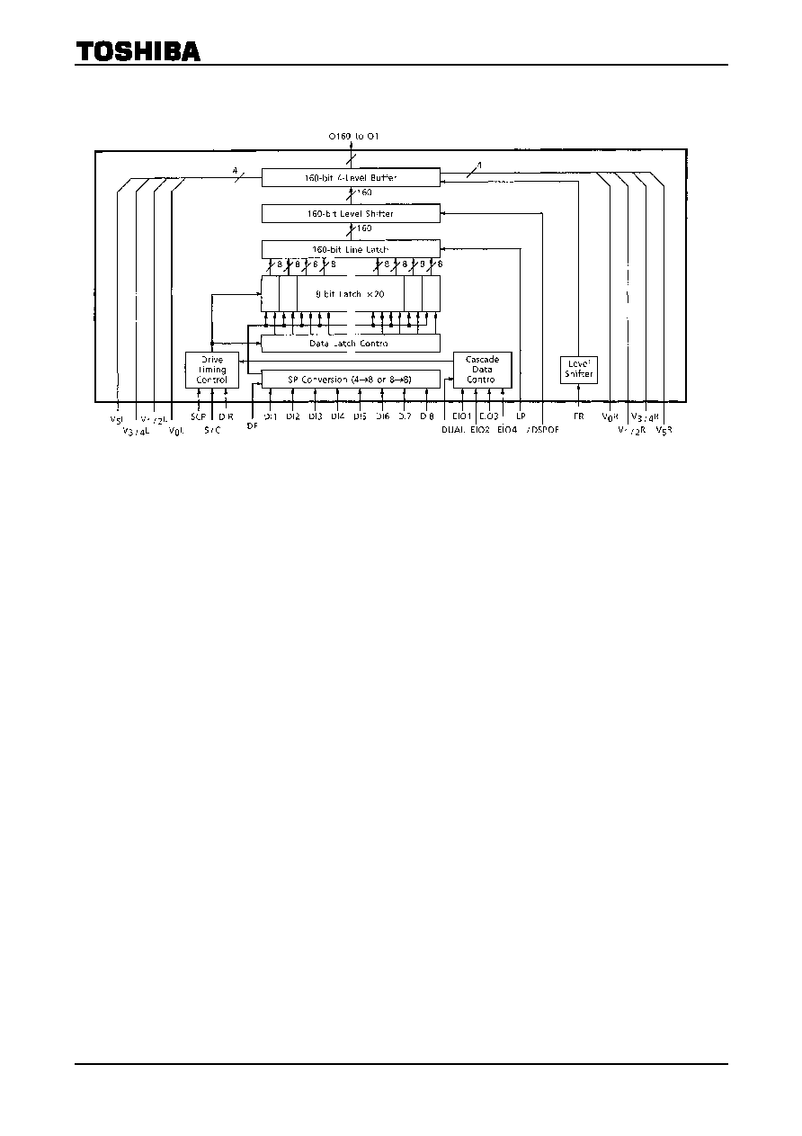
BLOCK DIAGRAM
T6C25
2000-12-05 3/11
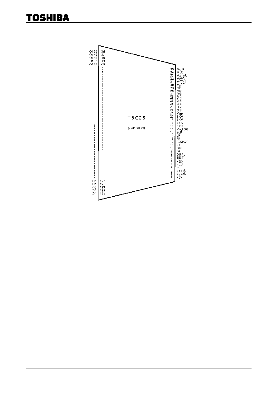
PIN ASSIGNMENT
* : The above diagram shows the pin configuration of the LSI Chip, not that of the tape carrier package.

T6C25
2000-12-05 4/11
PIN FUNCTIONS
PIN NAME
I / O
FUNCTIONS
LEVEL
O1 to O160
Output
Output for LCD drive signal
V
0
to V5
EIO1, EIO4
I / O
Input / output for enable signal
DIR selects In or Out.
Connect EIO (IN) of 1st LSI to L.
For a cascade connection, connect EIO (OUT) to EIO (IN) of next LSI.
(Column mode)
Input
for
data
signal
DI1 to DI8
Input
(Row mode)
Fix to H or L
DIR Input
(Direction)
Input for data flow direction select,
/ DSPOF
Input
(Display Off)
/ DSPOF = L : Display-off mode, (O1 to O160) remain at the V
5
level.
/ DSPOF = H : Display-on mode, (O1 to O160) are operational.
(Column mode)
Input for data bit select
DF Input
(Row mode)
Fix to H or L
(Column mode)
Fix to H or L
DUAL Input
(Row mode)
Input for dual / single select
(Column mode)
Display data is latched on falling edges of LP.
When EIO (IN) = L, setting
SCP
∑LP = H enables the 1st LSI.
LP
(Row mode)
Input for shift clock pulse
FR Input
(Frame)
Input for frame signal
(Column mode)
Input for shift clock pulse
SCP Input
(Row mode)
Fix to H or L
TEST Input
(TEST)
Fix
to
L
S / C
Input
Input for mode select : H = Column mode, L = Row mode
V
DD
to V
SS
VDD
Power supply for internal logic (+5.0 V)
VSS
Power supply for internal logic (0 V)
V
5
L∑R
Power supply for LCD drive circuit
V
3 / 4
L∑R
Power supply for LCD drive circuit
V
2 / 1
L∑R
Power supply for LCD drive circuit
V
0
L∑R
Power supply for LCD drive circuit
V
CC
L∑R
Power supply for LCD drive circuit
T6C25
2000-12-05 5/11
RELATION BETWEEN FR, DATA INPUT AND OUTPUT LEVEL
F R
DATA INPUT (DI1 to DI8)
/ DSPOF
OUTPUT LEVEL
(CULUMN MODE)
OUTPUT LEVEL
(ROW MODE)
L L H
V
3
V
4
L H H
V
5
V
0
H L H
V
2
V
1
H H H
V
0
V
5
*
*
L V
5
V
5
* : Don't Care
DATA INPUT FORMAT
Column mode
ENABLE PIN
INPUT DATA LINE AND OUTPUT BUFFERS
DIR DF BIT
MODE
EIO1 EIO2
(*1)
DI1 DI2 DI3 DI4 DI5 DI6 DI7 DI8
L O160
O159
O158
O157
H OUT
IN
F O4 O3 O2 O1
L O1 O2 O3 O4
L
L 4-BIT
IN OUT
F O157
O158
O159
O160
L O160
O159
O158
O157
O156 O155 O154
O153
H OUT
IN
F O8 O7 O6 O5 O4 O3 O2 O1
L O1 O2 O3 O4 O5 O6 O7 O8
L
H 8-BIT
IN OUT
F O153
O154
O155
O156
O157 O158 O159
O160
*1 :
L: Last Data
F: First Data
Row Mode
DATA INPUT TERMINALS
DUAL DIR
DATA
FLOW
EIO1 EIO2 EIO3 DIN
L L
O160
O1
OUT
IN
L H
O1
O160
IN
OUT
H L
O160 O81
O80 O1
OUT IN OUT IN
H H
O1 O80
O81 O160
IN OUT IN OUT
T6C25
200
0-
12-
0
5
6/
11
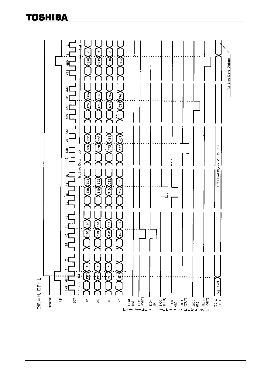
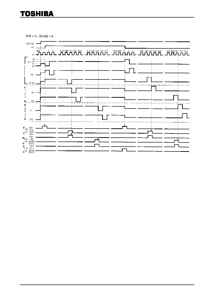
TIMING DIAGRAM (Column mode)
T6C25
2000-12-05 7/11
TIMING DIAGRAM
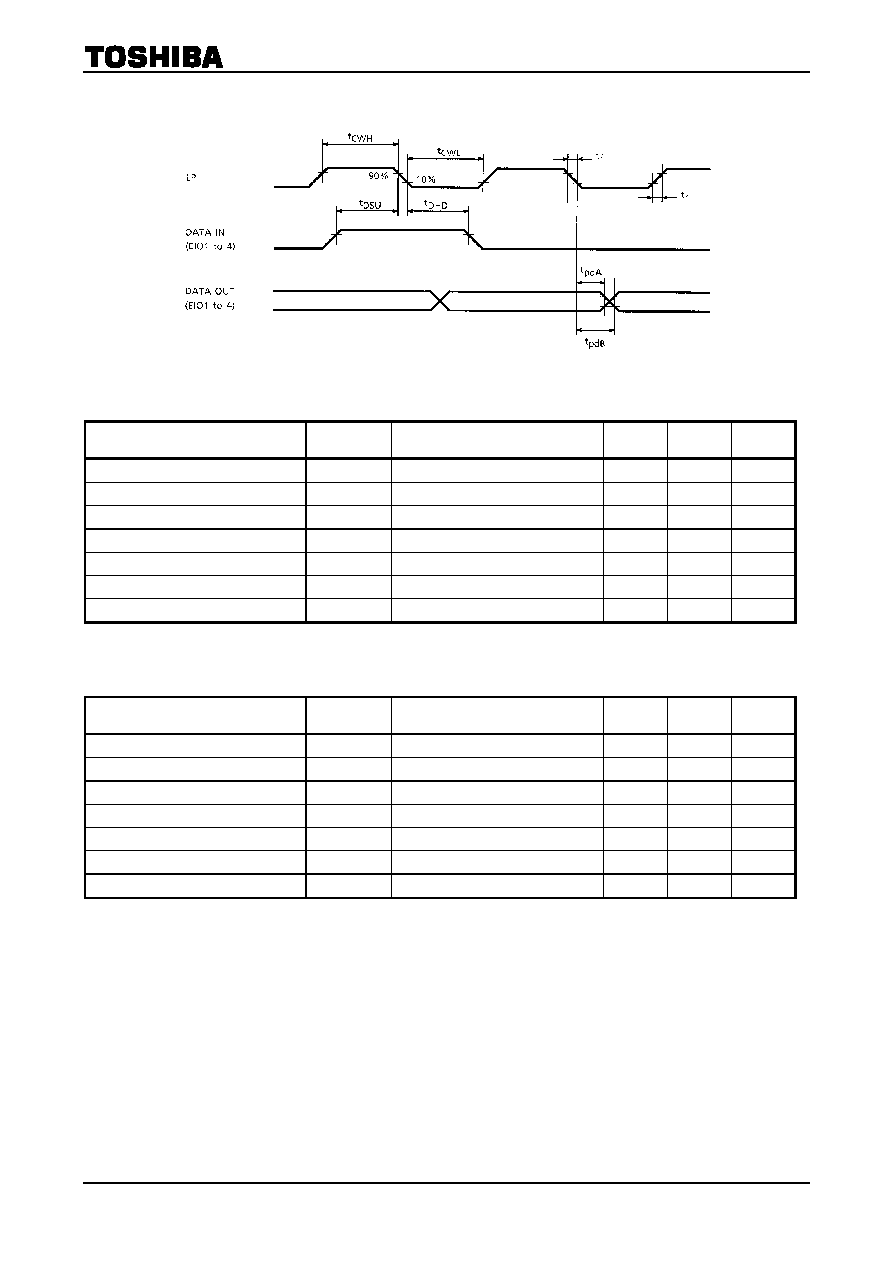
(Row mode)
T6C25
2000-12-05 8/11
ABSOLUTE MAXIMUM RATINGS
(Ensure that the following conditions are maintained, V
CC
V
0
V
2
V
3
V
5
V
SS
)
ITEM SYMBOL
PIN
NAME
RATING UNIT
Supply Voltage (1)
V
DD
V
DD
-0.3 to 7.0
V
Supply Voltage (2)
V
CC
V
CCL / R
- 0.3 to 45.0
V
Supply Voltage (3)
V
0
, V
2
V
0L / R,
V
2L / R
-0.3 to V
CC
+ 0.3
V
Supply Voltage (4)
V
3
, V
5
V
3L / R,
V
5L / R
-0.3 to 7.0
V
Input Voltage
V
IN
(*2)
-0.3 to V
DD
+ 0.3
V
Operating Temperature
T
opr
- 20 to 75
∞C
Storage Temperature
T
stg
- 40 to 125
∞C
*2 : SCP, FR, LP, DIR, DF, DUAL, S / C, EIO1 to 4, DI1 to 8, / DSPOF, TEST
ELECTRICAL CHARACTERISTICS
DC CHARACTERISTICS
(Unless otherwise noted, V
SS
= 0V, V
DD
= 2.7 to 5.5V, Ta = -20 to 75∞C)
ITEM SYMBOL
TEST
CIR-
CUIT
TEST CONDITION
MIN
TYP.
MAX
UNIT
PIN NAME
Supply Voltage 1
V
DD
2.7
5.0
5.5
V
DD
Supply Voltage 2
V
CC
14
42
V
CCL / R
H Level
V
IH
0.8
V
DD
V
DD
Input
Voltage
L Level
V
IL
(*2)
0
0.2
V
DD
SCP, FR, LP,
DIR, DF, DUAL
S / C, EIO1 to 4,
DI1 to 8,
/ DSPOF, TEST,
H Level
V
OH
I
OH
= -0.4 mA
V
DD
-0.5
V
DD
Output
Voltage
L Level
V
OL
I
OL
= 0.4 mA
0
1.3
V
EIO1, to 4
H Level
R
OH
V
OUT
= V
0
- 0.5 V
(*3)
0.6 1.3
V
OUT
= V
2
± 0.5 V
(*3)
0.6 1.3
M Level
R
OM
V
OUT
= V
3
± 0.5 V
(*3)
0.6 1.3
Output
Resistance
L Level
R
OL
V
OUT
= V
5
+ 0.5 V
(*3)
0.6 1.3
k O1
to
O160
Current
Consumption (*4)
I
DD
V
DD
= 5.5 V
V
CC
= 42 V
f
FR
= 40 Hz
f
scp
= 8.0 MHz
Input Data : every bit inverted
V
IH
= 5.5 V, V
IL
= 0 V
3.0 mA
V
DD
*3 : V
CC
= 20 V, 1 / 13 bias
*4 : Current consumption while the internal data receiver is operating.
T6C25
2000-12-05 9/11
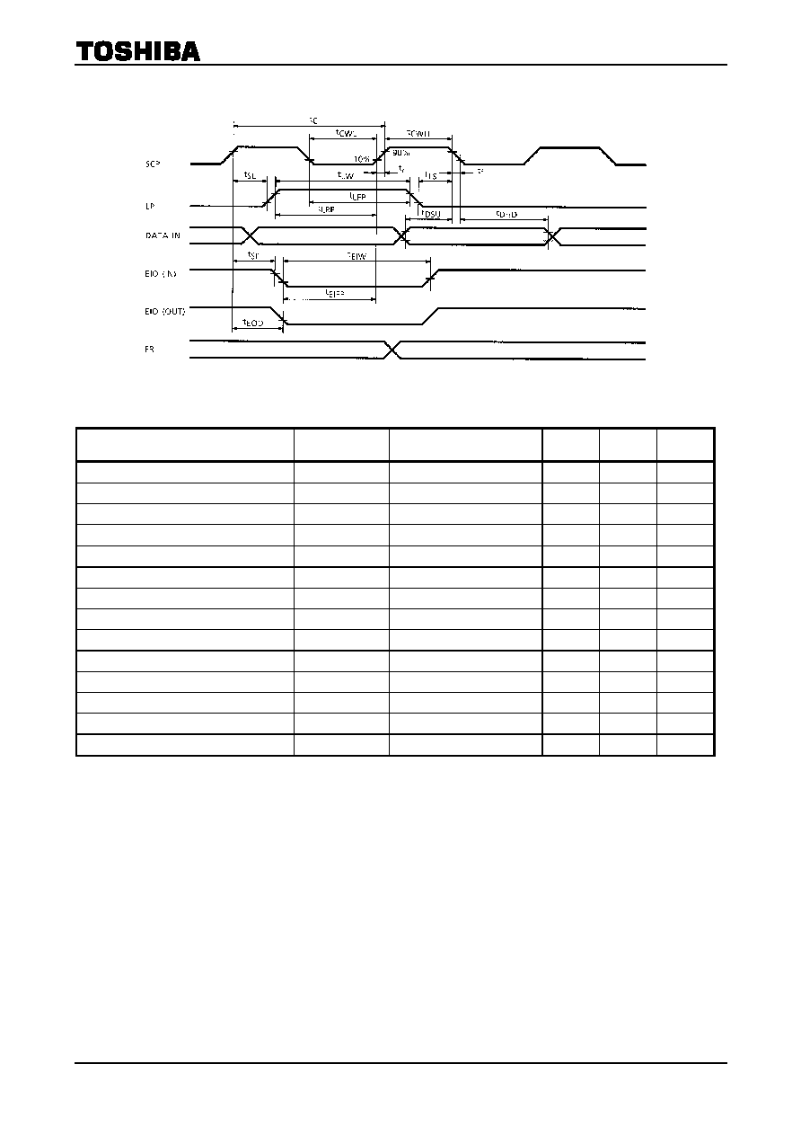
AC ELECTRICAL CHARACTERISTICS
(Column Mode)
TEST CONDITIONS (1)
(V
SS
= 0 V, V
DD
= 4.5 to 5.5 V, V
CC
= 14 to 42 V, Ta = -20 to 75∞C)
ITEM SYMBOL
TEST
CONDITION
MIN
MAX
UNIT
Clock Cycle
t
C
125
ns
SCP Pulse Width
t
CWH
, t
CWL
50
ns
Data Set-up Time
t
DSU
50
ns
Data Hold Time
t
DHD
50
ns
SCP Rise / Fall Time
t
r
, t
f
(*5) ns
LP Rise Time
t
LRP
50
ns
LP Fall Time
t
LFP
50
ns
LP Pulse Width
t
LW
45
ns
SCP-to-LP Delay Time
t
SL
40
ns
LP-to-SCP Delay Time
t
LS
40
ns
EIO-In Fall Time
t
EIFP
40
ns
EIO-In Pulse Width
t
EIW
40
ns
SCP-to-EIO Delay Time
t
SE
20
ns
EIO-Out Delay Time
t
EOD
(*6)
80 ns
*5 : t
r
, t
f
(t
C
- t
CWH
- t
CWL
) / 2 and t
r
, t
f
50 ns
*6 : C
L
= 30 pF
T6C25
2000-12-05 10/11
TEST CONDITIONS (2)
(V
SS
= 0 V, V
DD
= 2.7 to 4.5 V, V
CC
= 14 to 42 V, Ta = -20 to 75∞C)
ITEM SYMBOL
TEST
CONDITION
MIN
MAX
UNIT
Clock Cycle
t
C
500
ns
SCP Pulse Width
t
CWH
, t
CWL
240
ns
Data Set-up Time
t
DSU
240
ns
Data Hold Time
t
DHD
240
ns
SCP Rise / Fall Time
t
r
, t
f
(*5) ns
LP Rise Time
t
LRP
240
ns
LP Fall Time
t
LFP
240
ns
LP Pulse Width
t
LW
240
ns
SCP-to-LP Delay Time
t
SL
50
ns
LP-to-SCP Delay Time
t
LS
100
ns
EIO-In Fall Time
t
EIFP
240
ns
EIO-In Pulse Width
t
EIW
240
ns
SCP-to-EIO Delay Time
t
SE
50
ns
EIO-Out Delay Time
t
EOD
(*6)
260 ns
*5 : t
r
, t
f
(t
C
- t
CWH
- t
CWL
) / 2 and t
r
, t
f
50 ns
*6 : C
L
= 30 pF
T6C25
2000-12-05 11/11
AC ELECTRICAL CHARACTERISTICS
(Row mode)
TEST CONDITIONS (1)
(V
SS
= 0 V, V
DD
= 4.5 to 5.5 V, V
CC
= 14 to 42 V, Ta = -20 to 75∞C)
ITEM SYMBOL
TEST
CONDITION
MIN
MAX
UNIT
LP Pulse Width H
t
CWH
LP
30
ns
LP Pulse Width L
t
CWL
LP
195
ns
SCP Rise / Fall Time
t
r
, t
f
LP, FR, EIO1 to 4
20 ns
Data Set-up Time
t
DSU
EIO1 to 4
80
ns
Data Hold Time
t
DHD
EIO1 to 4
0
ns
EIO-Out Delay Time A (*7) t
pdA
EIO1 to 4
5
ns
EIO-Out Delay Time B (*7) t
pdB
EIO1 to 4
150 ns
TEST CONDITIONS (2)
(V
SS
= 0 V, V
DD
= 2.7 to 5.5 V, V
CC
= 14 to 42 V, Ta = -20 to 75∞C)
ITEM SYMBOL
TEST
CONDITION
MIN
MAX
UNIT
LP Pulse Width H
t
CWH
LP 100
ns
LP Pulse Width L
t
CWL
LP
400
ns
SCP Rise / Fall Time
t
r
, t
f
LP, FR, EIO1 to 4
20 ns
Data Set-up Time
t
DSU
EIO1 to 4
130
ns
Data Hold Time
t
DHD
EIO1 to 4
0
ns
EIO-Out Delay Time A (*7)
t
pdA
EIO1 to 4
5
ns
EIO-Out Delay Time B (*7)
t
pdB
EIO1 to 4
400 ns
*7 :
C
L
= 30 pF
Note : Insert the bypass capacitor (0.1µF) between V
DD
and V
SS
to decrease power supply noise.
Place the bypass capacitor as close to the LSI as possible.