 | –≠–ª–µ–∫—Ç—Ä–æ–Ω–Ω—ã–π –∫–æ–º–ø–æ–Ω–µ–Ω—Ç: T6K11 | –°–∫–∞—á–∞—Ç—å:  PDF PDF  ZIP ZIP |
T6K11
2001-03-13 1/47
TOSHIBA CMOS DIGITAL INTEGRATED CIRCUIT SILICON MONOLITHIC
T6K11
DOT MATRIX LCD DRIVER
The T6K11 driver is designed for use in small to medium-sized
dot matrix LCD panels. This driver can be interfaced to the MPU
via a 4 / 8-bit (68 / 80-series) or a serial interface, and is
operated asynchronously with the MPU. Since the T6K11
contains an CR circuit clock driver, it can generate the timing
signals required for the LCD.
The display data can be stored in the built-in display RAM,
whose cells each correspond to each dot on the dot-matrix LCD.
The display data written to the RAM corresponds one for one to
the LCD drive signals output by the device. Since the T6K11 has
160 outputs for the LCD drive (segment) signals that constitute
display data and 65 outputs for the LCD drive (common) signals
that constitute scanning signals, this single device allows you to
drive an LCD panel comprised of up to 160 ◊ 65 dots with a
minimum of power requirement.
To minimize its power consumption, the T6K11 has a display
change mode (power save mode) in which only a 160 ◊ 1-dot icon can be displayed. What's more, it has various
built-in analog circuits such as a D / A converter for the LCD drive power supply, a step-up circuit (◊2 to ◊5), and
a contrast control (electronic VR) circuit. All these circuits enable the LCD panel to be driven with a single power
supply.
This product is under development; hence, specifications may change without notice. When you use this product,
please refer to the latest technical datasheet.
∑ TOSHIBA is continually working to improve the quality and reliability of its products. Nevertheless, semiconductor devices in general
can malfunction or fail due to their inherent electrical sensitivity and vulnerability to physical stress. It is the responsibility of the
buyer, when utilizing TOSHIBA products, to comply with the standards of safety in making a safe design for the entire system, and
to avoid situations in which a malfunction or failure of such TOSHIBA products could cause loss of human life, bodily injury or
damage to property.
In developing your designs, please ensure that TOSHIBA products are used within specified operating ranges as set forth in the
most recent TOSHIBA products specifications. Also, please keep in mind the precautions and conditions set forth in the "Handling
Guide for Semiconductor Devices," or "TOSHIBA Semiconductor Reliability Handbook" etc..
∑ The TOSHIBA products listed in this document are intended for usage in general electronics applications (computer, personal
equipment, office equipment, measuring equipment, industrial robotics, domestic appliances, etc.). These TOSHIBA products are
neither intended nor warranted for usage in equipment that requires extraordinarily high quality and/or reliability or a malfunction or
failure of which may cause loss of human life or bodily injury ("Unintended Usage"). Unintended Usage include atomic energy
control instruments, airplane or spaceship instruments, transportation instruments, traffic signal instruments, combustion control
instruments, medical instruments, all types of safety devices, etc.. Unintended Usage of TOSHIBA products listed in this document
shall be made at the customer's own risk.
∑ Polyimide base film is hard and thin. Be careful not to injure yourself on the film or to scratch any other parts with the film. Try to
design and manufacture products so that there is no chance of users touching the film after assembly, or if they do , that there is no
chance of them injuring themselves. When cutting out the film, try to ensure that the film shavings do not cause accidents. After use,
treat the leftover film and reel spacers as industrial waste.
∑ Light striking a semiconductor device generates electromotive force due to photoelectric effects. In some cases this can cause the
device to malfunction.
This is especially true for devices in which the surface (back), or side of the chip is exposed. When designing circuits, make sure
that devices are protected against incident light from external sources. Exposure to light both during regular operation and during
inspection must be taken into account.
∑ The products described in this document are subject to the foreign exchange and foreign trade laws.
∑ The information contained herein is presented only as a guide for the applications of our products. No responsibility is assumed by
TOSHIBA CORPORATION for any infringements of intellectual property or other rights of the third parties which may result from its
use. No license is granted by implication or otherwise under any intellectual property or other rights of TOSHIBA CORPORATION or
others.
∑ The information contained herein is subject to change without notice.
000707EBE1

T6K11
2001-03-13 2/47
Features
l Display RAM
: 160 (64 + 1) = 10,400 bits
l LCD drive outputs
: 160 segment outputs
65 common outputs (including one common output for icon)
l RAM data direct display : Turned on when bit data in RAM = 1
Turned off when bit data in RAM = 0
l Display duty cycle
: 1/2 duty during power save mode
1/35, 1/49, 1/57, or 1/65 duty during normal mode
(Duty cycles in normal mode are set in software by the MPU.)
l Display modes
: Normal mode ............. Full display
Power save mode ....... Icon display
Standby mode ............ Clock stop (all internal circuits turned off)
l MPU :
8-bit (68 / 80 series) parallel or serial interface
l Oscillator :
Built-in CR oscillator (resistor and capacitor completely built-in), external clock
input acceptable
l Power supply circuits
: D/A converter for LCD drive power supply (temperature derating = 0.20% / ∞C),
step-up circuit (◊2 to ◊5), contrast control circuit
l Operating voltages
: AV
DD
(used for analog) = DV
DD
to 5.5 V
DV
DD
(used for digital) = 1.8 to 3.3 V
l LCD drive voltage
: V
CC
= 16.5 V (max)
l CMOS process
l Low power consumption : ISS = 103 µA (typ.)
Conditions: AV
DD
= DV
DD
= 3.0 V, step-up circuit used (◊4 mode), LCD nonloaded,
Ta = 25∞C, display data = all "checker pattern," no data access from
MPU
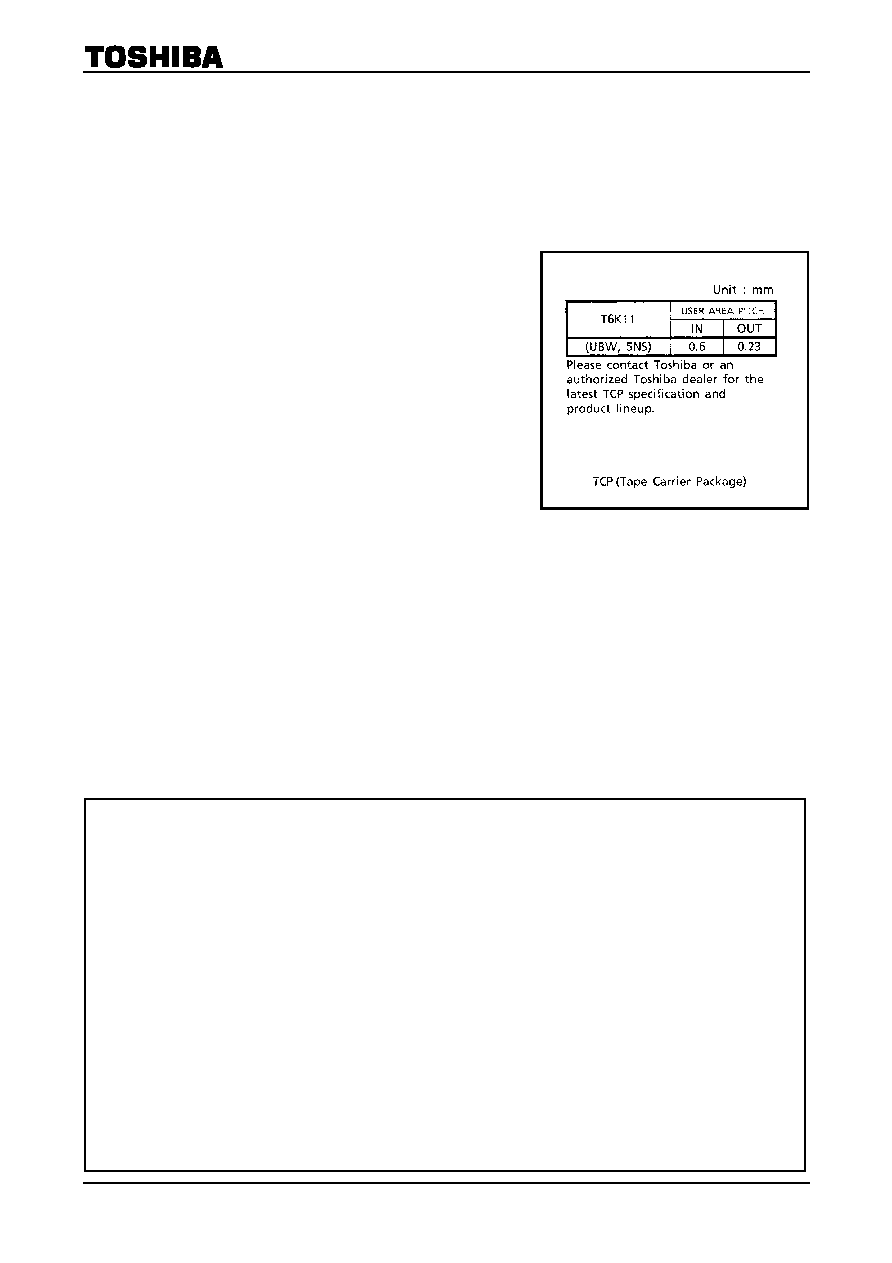
l Package :
Product Package
T6K11(XXX, XXX)
TCP (Tape carrier package)
JBT6K11-AS Gold
Bump
Chip

T6K11
2001-03-13 3/47
B
l
ock D
i
agr
a
m

T6K11
2001-03-13 4/47
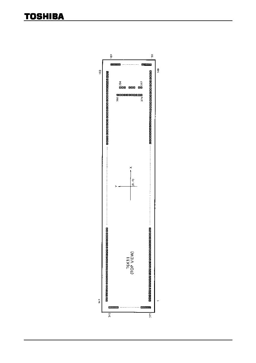
Pin Assignment
Note: The above TCP pin assignment is shown for reference purposes only.
T6K11
2001-03-13 5/47
Pad Specification
Item Size
Unit
Chip size
10360 ◊ 2550
mm
(1)
-5180 , -1275
(2)
-5180 , 1275
(3) 5180 , 1275
Chip tip coordinates
(4) 5180 , -1275
mm
Bump pitch
60
mm
Bump height
14 ± 4
mm
Item Number
of
pins
Input pin
116 pin (including dummy pins)
Output pin
226 pin (including dummy pins)
Fuse pin
33 pin (including dummy pins)
(Note 1)
Test pin
19 pin
(Note 1)
(Note 1): Fuse (No.117 to 149) and Test (No.376 to 394) are LSI test pins, leave these pins open.
T6K11
2001-03-13 6/47
P
a
d
L
ayou
t

T6K11
2001-03-13 7/47
Pad Coordinates
(Unit: µm)
No.
Name X
Y
No.
Name X Y
No.
Name X Y
1 DV
DD
-4753
-1090 41 AV
SS
-2176
-1090 81
V
LC0
384
-1090
2 /STB -4672
-1090 42 AV
SS
-2112
-1090 82
V
LC0
448
-1090
3 DV
SS
-4608
-1090 43
DUMMY5
-2048
-1090 83
V
LC1
512
-1090
4 /CS1 -4544
-1090 44 AV
DD
-1984
-1090 84
V
LC1
576
-1090
5 CS2 -4480
-1090 45 AV
DD
-1920
-1090 85
V
LC2
640
-1090
6 DV
DD
-4416
-1090 46 AVDD -1856
-1090 86
V
LC2
704
-1090
7 /RST -4352
-1090 47 AV
DD
-1792
-1090 87
DUMMY9 768
-1090
8 DUMMY1 -4288
-1090 48
DUMMY6
-1728
-1090 88
V
LC3
832
-1090
9 RS -4224
-1090 49 C1A -1664
-1090 89
V
LC3
896
-1090
10 DV
SS
-4160
-1090 50 C1A -1600
-1090 90
V
LC4
960
-1090
11 /WR -4096
-1090 51 C1B -1536
-1090 91
V
LC4
1024
-1090
12 /RD -4032
-1090 52 C1B -1472
-1090 92
V
LC5
1088
-1090
13 DV
DD
-3968
-1090 53 V
OUT1
-1408
-1090 93
V
LC5
1152
-1090
14 DB0 -3904
-1090 54 V
OUT1
-1344
-1090 94 DUMMY10 1216 -1090
15 DB1 -3840
-1090 55 C2A -1280
-1090 95
AV
SS
1280
-1090
16 DB2 -3776
-1090 56 C2A -1216
-1090 96 DUMMY11 1344 -1090
17 DB3 -3712
-1090 57 C2B -1152
-1090 97
DV
SS
1408
-1090
18 DB4 -3648
-1090 58 C2B -1088
-1090 98
68/80 1472 -1090
19 DB5 -3584
-1090 59 V
OUT2
-1024
-1090 99
DV
DD
1536
-1090
20 DB6 -3520
-1090 60 V
OUT2
-960
-1090 100
P/S
1600
-1090
21 DB7 -3456
-1090 61 C3A
-896
-1090 101
DV
SS
1664
-1090
22 DUMMY2 -3392
-1090 62 C3A
-832
-1090 102 DUMMY12 1728
-1090
23 DV
DD
-3328
-1090 63 C3B
-768
-1090 103 DUMMY13 1792
-1090
24 DV
DD
-3264
-1090 64 C3B
-704
-1090 104 DUMMY14 1856
-1090
25 DV
DD
-3200
-1090 65 V
OUT3
-640
-1090 105 DUMMY15 1920
-1090
26 DV
DD
-3136
-1090 66 V
OUT3
-576
-1090 106 DUMMY16 1984
-1090
27 DV
DD
-3072
-1090 67 C4A
-512
-1090 107 DUMMY17 2048
-1090
28 DUMMY3 -3008
-1090 68 C4A
-448
-1090 108 DUMMY18 2112
-1090
29 DV
SS
-2944
-1090 69 C4B
-384
-1090 109 DUMMY19 2176
-1090
30 DV
SS
-2880
-1090 70 C4B
-320
-1090 110 DUMMY20 2240
-1090
31 DV
SS
-2816
-1090 71 V
OUT4
-256
-1090 111 DUMMY21 2304
-1090
32 DV
SS
-2752
-1090 72 V
OUT4
-192
-1090 112 DUMMY22 2368
-1090
33 DV
SS
-2688
-1090 73 V
CC
-128
-1090 113 DUMMY23 2432
-1090
34 CL -2624
-1090 74 V
CC
-64
-1090 114 DUMMY24 2496
-1090
35 DV
DD
-2560
-1090 75 V
CC
0
-1090 115
OSCV
DD
2560
-1090
36 CLS -2496
-1090 76 V
CC
64
-1090 116
VREG
2624
-1090
37 DV
SS
-2432
-1090 77
DUMMY7
128
-1090 117 DUMMY25 2688
-1090
38 DUMMY4 -2368
-1090 78 AV
SS
192
-1090 118
FUSE1 2752
-1090
39 AV
SS
-2304
-1090 79 AV
SS
256
-1090 119 DUMMY26 2816
-1090
40 AV
SS
-2240
-1090 80
DUMMY8
320
-1090 120
FUSE2 2880
-1090

T6K11
2001-03-13 8/47
(Unit: µm)
No.
Name X
Y
No.
Name X Y
No.
Name X Y
121 DUMMY27
2944
-1090 161 COM21
4988
-410 201
SEG19 3690
1083
122 FUSE3
3008
-1090 162 COM20
4988
-350 202
SEG20 3630
1083
123 DUMMY28
3072
-1090 163 COM19
4988
-290 203
SEG21 3570
1083
124 FUSE4
3136
-1090 164 COM18
4988
-230 204
SEG22 3510
1083
125 DUMMY29
3200
-1090 165 COM17
4988
-170 205
SEG23 3450
1083
126 FUSE5
3264
-1090 166 COM16
4988
-110 206
SEG24 3390
1083
127 DUMMY30
3328
-1090 167 COM15
4988
-50 207
SEG25 3330 1083
128 FUSE6
3392
-1090 168 COM14
4988
10 208
SEG26 3270
1083
129 DUMMY31
3456
-1090 169 COM13
4988
70 209
SEG27 3210
1083
130 FUSE7
3520
-1090 170 COM12
4988
130 210
SEG28 3150
1083
131 DUMMY32
3584
-1090 171 COM11
4988
190 211
SEG29 3090
1083
132 FUSE8
3648
-1090 172 COM10
4988
250 212
SEG30 3030
1083
133 DUMMY33
3712
-1090 173 COM9
4988
310 213
SEG31 2970
1083
134 FUSE9
3776
-1090 174 COM8
4988
370 214
SEG32 2910
1083
135 DUMMY34
3840
-1090 175 COM7
4988
430 215
SEG33 2850
1083
136 FUSE10
3904
-1090 176 COM6
4988
490 216
SEG34 2790
1083
137 DUMMY35
3968
-1090 177 COM5
4988
550 217
SEG35 2730
1083
138 FUSE11
4032
-1090 178 COM4
4988
610 218
SEG36 2670
1083
139 DUMMY36
4096
-1090 179 COM3
4988
670 219
SEG37 2610
1083
140 FUSE12
4160
-1090 180 COM2
4988
730 220
SEG38 2550
1083
141 DUMMY37
4224
-1090 181 COM1
4988
790 221
SEG39 2490
1083
142 FUSE13
4288
-1090 182 ICONA 4988
870 222
SEG40 2430
1083
143 DUMMY38
4352
-1090
183
SEG1 4790 1083
223
SEG41 2370 1083
144 FUSE14
4416
-1090
184
SEG2 4710 1083
224
SEG42 2310 1083
145 DUMMY39
4480
-1090
185
SEG3 4650 1083
225
SEG43 2250 1083
146 FUSE15
4544
-1090
186
SEG4 4590 1083
226
SEG44 2190 1083
147 FUSE16
4608
-1090
187
SEG5 4530 1083
227
SEG45 2130 1083
148 DUMMY40
4672
-1090
188
SEG6 4470 1083
228
SEG46 2070 1083
149 FUSE17
4753
-1090
189
SEG7 4410 1083
229
SEG47 2010 1083
150 COM32
4988
-1090
190
SEG8 4350 1083
230
SEG48 1950 1083
151 COM31
4988
-1010
191
SEG9 4290 1083
231
SEG49 1890 1083
152 COM30
4988
-950
192
SEG10 4230 1083
232
SEG50 1830 1083
153 COM29
4988
-890
193
SEG11 4170 1083
233
SEG51 1770 1083
154 COM28
4988
-830
194
SEG12 4110 1083
234
SEG52 1710 1083
155 COM27
4988
-770
195
SEG13 4050 1083
235
SEG53 1650 1083
156 COM26
4988
-710
196
SEG14 3990 1083
236
SEG54 1590 1083
157 COM25
4988
-650
197
SEG15 3930 1083
237
SEG55 1530 1083
158 COM24
4988
-590
198
SEG16 3870 1083
238
SEG56 1470 1083
159 COM23
4988
-530
199
SEG17 3810 1083
239
SEG57 1410 1083
160 COM22
4988
-470
200
SEG18 3750 1083
240
SEG58 1350 1083
T6K11
2001-03-13 9/47
(Unit: µm)
No.
Name X
Y
No.
Name X Y
No.
Name X Y
241 SEG59
1290
1083 281 SEG99 -1110 1083
321
SEG139
-3510 1083
242 SEG60
1230
1083 282 SEG100
-1170 1083
322
SEG140
-3570 1083
243 SEG61
1170
1083 283 SEG101
-1230 1083
323
SEG141
-3630 1083
244 SEG62
1110
1083 284 SEG102
-1290 1083
324
SEG142
-3690 1083
245 SEG63
1050
1083 285 SEG103
-1350 1083
325
SEG143
-3750 1083
246 SEG64
990
1083 286 SEG104
-1410 1083
326
SEG144
-3810 1083
247 SEG65
930
1083 287 SEG105
-1470 1083
327
SEG145
-3870 1083
248 SEG66
870
1083 288 SEG106
-1530 1083
328
SEG146
-3930 1083
249 SEG67
810
1083 289 SEG107
-1590 1083
329
SEG147
-3990 1083
250 SEG68
750
1083 290 SEG108
-1650 1083
330
SEG148
-4050 1083
251 SEG69
690
1083 291 SEG109
-1710 1083
331
SEG149
-4110 1083
252 SEG70
630
1083 292 SEG110
-1770 1083
332
SEG150
-4170 1083
253 SEG71
570
1083 293 SEG111
-1830 1083
333
SEG151
-4230 1083
254 SEG72
510
1083 294 SEG112
-1890 1083
334
SEG152
-4290 1083
255 SEG73
450
1083 295 SEG113
-1950 1083
335
SEG153
-4350 1083
256 SEG74
390
1083 296 SEG114
-2010 1083
336
SEG154
-4410 1083
257 SEG75
330
1083 297 SEG115
-2070 1083
337
SEG155
-4470 1083
258 SEG76
270
1083 298 SEG116
-2130 1083
338
SEG156
-4530 1083
259 SEG77
210
1083 299 SEG117
-2190 1083
339
SEG157
-4590 1083
260 SEG78
150
1083 300 SEG118
-2250 1083
340
SEG158
-4650 1083
261 SEG79
90
1083 301 SEG119
-2310 1083
341
SEG159
-4710 1083
262 SEG80
30
1083 302 SEG120
-2370 1083
342
SEG160
-4790 1083
263 SEG81
-30 1083
303
SEG121
-2430 1083
343
COM33
-4988 870
264 SEG82
-90 1083
304
SEG122
-2490 1083
344
COM34
-4988 790
265 SEG83
-150 1083
305
SEG123
-2550 1083
345
COM35
-4988 730
266 SEG84
-210 1083
306
SEG124
-2610 1083
346
COM36
-4988 670
267 SEG85
-270 1083
307
SEG125
-2670 1083
347
COM37
-4988 610
268 SEG86
-330 1083
308
SEG126
-2730 1083
348
COM38
-4988 550
269 SEG87
-390 1083
309
SEG127
-2790 1083
349
COM39
-4988 490
270 SEG88
-450 1083
310
SEG128
-2850 1083
350
COM40
-4988 430
271 SEG89
-510 1083
311
SEG129
-2910 1083
351
COM41
-4988 370
272 SEG90
-570 1083
312
SEG130
-2970 1083
352
COM42
-4988 310
273 SEG91
-630 1083
313
SEG131
-3030 1083
353
COM43
-4988 250
274 SEG92
-690 1083
314
SEG132
-3090 1083
354
COM44
-4988 190
275 SEG93
-750 1083
315
SEG133
-3150 1083
355
COM45
-4988 130
276 SEG94
-810 1083
316
SEG134
-3210 1083
356
COM46
-4988 70
277 SEG95
-870 1083
317
SEG135
-3270 1083
357
COM47
-4988 10
278 SEG96
-930 1083
318
SEG136
-3330 1083
358
COM48
-4988
-50
279 SEG97
-990 1083
319
SEG137
-3390 1083
359
COM49
-4988
-110
280 SEG98 -1050 1083
320
SEG138
-3450 1083
360
COM50
-4988
-170

T6K11
2001-03-13 10/47
(Unit: µm)
No.
Name X
Y
No.
Name X Y
No.
Name X Y
361 COM51 -4988
-230 373
COM63
-4988
-950 385
TEST10 3575
339
362 COM52 -4988
-290 374
COM64
-4988
-1010 386
TEST11 3575
439
363 COM53 -4988
-350 375 ICONB -4988
-1090 387
TEST12 3795
-573
364 COM54 -4988
-410 376 TEST1 3575
-573 388
TEST13 3795
-473
365 COM55 -4988
-470 377 TEST2 3575
-473 389
TEST14 3795
-261
366 COM56 -4988
-530 378 TEST3 3575
-373 390
TEST15 3795
-161
367 COM57 -4988
-590 379 TEST4 3575
-261 391
TEST16 3795
-61
368 COM58 -4988
-650 380 TEST5 3575
-161 392
TEST17 3795
139
369 COM59 -4988
-710 381 TEST6 3575
-61 393
TEST18 3795
239
370 COM60 -4988
-770 382 TEST7 3575
39 394
TEST19 3795
339
371 COM61 -4988
-830
383
TEST8
3575
139
372 COM62 -4988
-890
384
TEST9
3575
239
T6K11
2001-03-13 11/47
Pin Function
Pin Name
Pin No.
I/O
Function
SEG1~160
Output
LCD drive segment signals
COM1~64
Output
LCD drive common signals
ICON
Output
LCD drive common signal (used for icon)
DB0~DB5
I
/
O
Data bus
When P/S = low, DB0 to DB5 are placed in the high-impedance state.
DB6
(SCK)
I
/
O
Data bus
When P/S = low, this bus functions as the serial interface's data synchronizing clock
(SCK).
DB7
(SI)
I
/
O
Data bus
When P/S = low, this bus functions as the serial interface's data input pin (SI).
RS
Input
Register mode select signal
When RS = low, this input is recognized as a register number.
When RS = high, this input is recognized as the data to be written to the register.
/RD
(E)
Input
Read select signal
When 68/80 = low (80-series MPU selected), data is output while this pin is held
low. Data is latched in at the active edge.
When 68/80 = high (68-series MPU selected), this pin is used as an enable signal
input pin (E).
/WR
(R/W)
Input
Write select signal
When 68/80 = low (80-series MPU selected), data is latched at the rising edge of
/WR.
When 68/80 = high (68-series MPU selected), data read is selected if R/W = high
or data write is selected if R/W = low.
/CS1
Input
Chip select signal (1)
Data/commands can be input or output while this signal is held low.
CS2
Input
Chip select signal (2)
Data/commands can be input or output while this signal is held high.
/RST
Input
Reset signal
The device is reset when this signal is pulled low.
P/S
Input
Parallel/serial interface select signal
The parallel interface is selected when this signal is high.
The serial interface is selected when this signal is low.
68/80
Input
68/80-series parallel MPU select signal
The 68-series parallel MPU is selected when this signal is high.
The 80-series parallel MPU is selected when this signal is low.
CLS
Input
CR oscillator circuit ON/OFF select signal
The internal CR oscillator is turned on when CLS is high.
The internal CR oscillator is turned off when CLS is low, allowing for an external
clock input to be used. In this case, use the CL pin to supply the external clock.
CL
I
/
O
Display clock input pin
When CLS = high, this pin functions as the internal CR circuit's clock monitor pin.
When CLS = low, this pin is used to input an external clock to the device.
/STB
Input
Standby signal
The device is placed in standby state when / STB is low.
C1A, C1B
External capacitor connecting pin for ◊2 step-up
VOUT1
◊2
step-up voltage output pin
C2A, C2B
External capacitor connecting pin for ◊3 step-up
VOUT2
◊3
step-up voltage output pin
C3A, C3B
External capacitor connecting pin for ◊4 step-up
VOUT3
◊4
step-up voltage output pin
C4A, C4B
External capacitor connecting pin for ◊5 step-up
VOUT4
◊5
step-up voltage output pin
VREG
LV regulator output pin
(Note 1)
V
CC
LCD drive power supply pin
(Note 1)

T6K11
2001-03-13 12/47
Pin Name
Pin No.
I/O
Function
VLC0 to VLC4
LCD drive power supply pin
(Note 1)
VLC5
LCD drive power supply pin: Connect to V
SS
OSCV
DD
CR oscillator circuit regulator output pin: Leave this pin open.
AV
DD
, AV
SS
Analog circuit power supply pin
DV
DD
, DV
SS
Digital circuit power supply pin
FUSE1 to 17
LSI Test pins: Leave these pins open.
TEST1 to 19
LSI Test pins: Leave these pins open.
(Note 1): Connect the capacitor between this pin and V
SS
.
T6K11
2001-03-13 13/47
Function Each Block
MPU interface unit
Depending on whether the 68/80 input and P/S input pins are high or low, the T6K11 selects an 8-bit
parallel or a serial interface, allowing for data to be transferred from the MPU.
P/S
68/80
Interface Type
/CS1
CS2
RS
/WR
/RD
DB7
DB6
DB5 to 0
80-series MPU
( /CS1)
/CS1
H
RS
/WR
/RD
DB7
DB6
DB5 to 0
L
80-series MPU
(CS2)
L
CS2
RS
/WR
/RD
DB7
DB6
DB5 to 0
H
H 68-series MPU
L
H
RS
R/W
E
DB7
DB6
DB5 to 0
L
Serial
L H RS
H/L
H/L SI
SCK Hi-Z
Note: "H" denotes the DV
DD
level; "L" denotes the DV
SS
level.

T6K11
2001-03-13 14/47
(a) For the 80-series MPU
(b) For the 68-series MPU
(c) For serial interface
Fig. 1

T6K11
2001-03-13 15/47
When the serial interface is selected (P / S = low), data and serial clock from the MPU are accepted providing
that / CS1 = low and CS2 = high. The serial data input to the device is taken in from SI in order of DB7, DB6,
◊◊◊DB0 at each rising edge of SCK, and are converted into parallel data at the 8th rising edge of SCK.
Recognition of the received data depends on the RS pin status at the 8th rising edge of SCK. If RS = low, the
data is recognized as a register number set; if RS = high, the data is recognized as write data. A serial
interface timing chart is shown in Fig. 2.
Note that when using the serial interface, the device can only write data to its internal logic and registers,
and cannot read data and status.
Fig. 2
Input / output buffer
This buffer is used to transfer data between the T6K11 and the MPU. For a parallel interface, this buffer is
used as an 8-bit data bus ; for a serial interface, it is used to receive serial data and serial clock, with the
serial data converted into parallel data before being taken into the internal circuit.
Input register
This register holds the data from the MPU. The data held in this register is recognized as a register number
or write data depending on whether RS is high or low.
Output register
This register holds 8-bit data when transferring display RAM data or status information to the MPU.
X-address counter
This counter is a 64-Up / Down counter used to hold the row address of the display RAM. When this counter
is selected by a command, it is automatically incremented or decremented each time data is read or written
to the display RAM.

T6K11
2001-03-13 16/47
Y-address counter
This counter is a 20-Up / Down counter used to hold the column address of the display RAM. When this
counter is selected by a command, it is automatically increased or decreased each time data is read or
written to the display RAM.
Z counter
This counter is a 64-Up counter used to supply the display data stored in the display RAM to the LCD drive
circuit. The data held in the Z-address register is loaded into this counter as Z-address. Therefore, if this
counter is set to 20, for example, it counts up from 20 to 21, 22, ◊◊◊62, 63, (icon) and from 0 to 1, 2, ◊◊◊18, 19, 20.
The start line on the LCD screen is line 20 of the display RAM. Note, however, that the icon line (64) cannot
be made the start line of the Z-address.
X / Y counter up / down register
This register holds the data that selects the up-count or down-count mode for the X and Y counters.
X / Y counter select register
This register holds the data that selects the X or Y counter to be used.
Display ON / OFF register
This 1-bit register holds the data that determines whether the display be turned on or off. When turned
OFF, outputs from the display RAM are reset. When turned ON, the display data corresponding to those in
the display RAM are output to the LCD. Since the data in the display RAM does not affect display ON/OFF
command control, the display RAM is not cleared anyway.
Z-address register
This 6-bit register holds the data that determines the display start line. By setting Z-address in this
register successively, it is possible to scroll the display up or down.
Oscillator
The clocking source can be switched between the built-in CR oscillator or an external clock depending on the
CLS pin status as shown in Fig. 3. When CLS = high, the CR oscillator is enabled, supplying display clock to
the internal logic. When CLS = low, the CL pin is switched for input, accepting an external clock.
Fig. 3
T6K11
2001-03-13 17/47
Timing signal generation circuit
This circuit generates the timing signals and operation clock required for display by dividing the clock
frequency derived from the CR circuit or an external source.
Shift registers
The T6K11 contains a 64-bit shift register necessary to shift the turn-on data required for the LCD drive
common signals and a 1-bit shift register used for the icon.
Duty cycle control register
This register holds the data that sets one of the four duty cycles that can be used.
Contrast control register
This register holds 4-stage VLC0 control data and 64-stage contrast control data.
Step-up circuit ON / OFF register
This register holds the data that determines whether the step-up circuit be turned on or off.
D / A converter ON / OFF register
This register holds the data that determines whether the D/A converter be turned on or off.
Bias control register
This register holds the data that sets one of the four bias values that can be used.
Latch circuit
This circuit latches display data from the RAM.
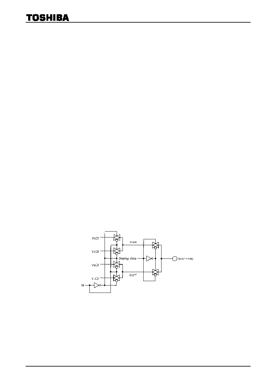
LCD drive circuit (segment)
The segment driver circuit consists of 160 drivers.
Each driver outputs one of the four LCD drive voltage levels depending on a combination of the display data
from the latch circuit and the M signal (used for FR) as shown in Fig. 4.
The segment driver circuit is shown below.
Fig. 4

T6K11
2001-03-13 18/47
LCD drive circuit (common)
The common driver circuit consists of 65 drivers. Each driver outputs one of the four LCD drive voltage
levels depending on a combination of the data from the shift register and the M signal (used for FR) as
shown in Fig. 5.
The common driver circuit is shown below.
Fig. 5
Step-up circuit
The T6K11 contains a ◊2/3/4/5 step-up circuit. When / RST = low or / STB = low, VOUT = 0 V (V
SS
level).
Normally, capacitors of more or less 2.2 µF are used for the step-up capacitor and step-up level retaining
capacitor. Since the step-up circuit power supply AV
DD
pin normally allows voltages to be input that are
higher than possible for the digital-block power supply DV
DD
pin, this circuit can generate the necessary
LCD drive voltage. However, because the rated LCD drive voltage is 16.5 V (max), care must be taken for the
voltage condition (AV
DD
voltage) used in step-up circuit and the number of boost steps to ensure that the
boosted voltage (the voltage output from VOUT) will not exceed the rated voltage of 16.5 V.
Note 1: Relationship of power supply voltages
.............. 5.5 V AV
DD
DV
DD
2.4 V
Note 2: Relationship between step-up output voltage and LCD drive voltage
.............. 16.5 V AV
DD
◊ n ( `n' denotes the number of boost steps.)
Example): When using a ◊5 step-up circuit
Fig. 6
T6K11
2001-03-13 19/47
Recommended Pin Processing When using a Step-up Circuit
Conditions
C1A, C1B VOUT1
C2A, C2B
VOUT2
C3A, C3B
VOUT3 C4A, C4B VOUT4
When using ◊2 step-up
circuit Available
Available
Open Open Open Open Open Open
When using ◊3 step-up
circuit Available
Available
Available
Available
Open Open Open Open
When using ◊4 step-up circuit
Available Available
Available
Open
Available
Available
Open
Open
When using ◊5 step-up
circuit
Available Available
Available
Open Available
Open Available Available
Note: "Available" means that a capacitor is connected to the pin.
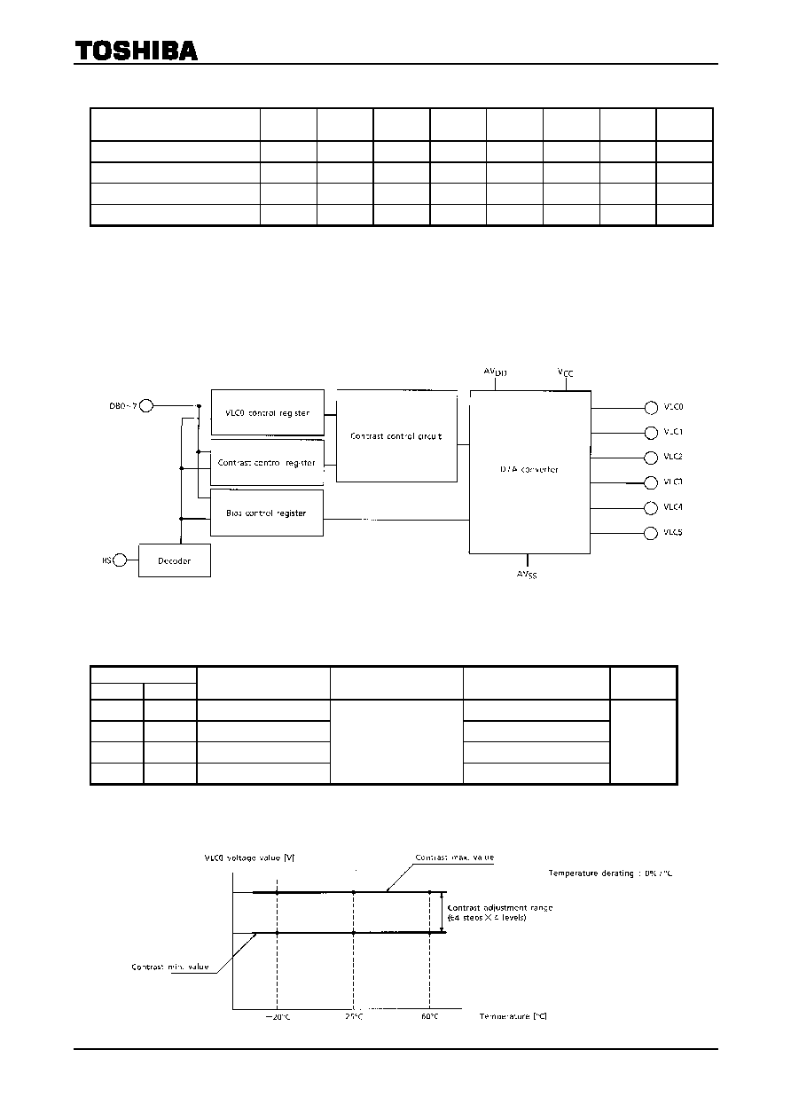
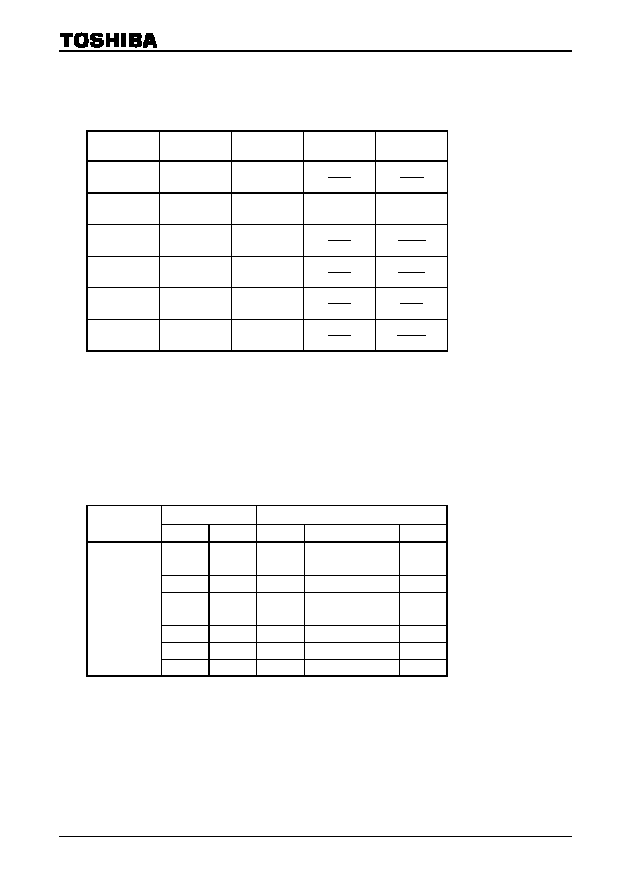
Contrast control, bias control, and D / A converter
The T6K11 contains a power supply generating circuit for LCD drive which is comprised of the D / A
converter. The contrast (electronic VR) and bias required for each type of LCD panel are controlled by this
circuit. Refer to Fig. 7 for a block diagram of this power supply circuit.
Fig. 7
Resistor Ratios for Adjusting LCD Drive Voltage
(VLC0)
VLC0 Control
DB7 DB6
VLC0 Voltage Typ. Value
(Max Contrast)
Number of Contrast Steps V
CC
Input Voltage Min Value
Remark
1 1
14.0
V
15.0
V
1 0
13.0
V
14.0
V
0 1
12.0
V
13.0
V
0 0
11.0
V
64 Steps
12.0 V
Ta = 25∞C
1/9 bias
(Note): The VLC0 voltage is derated with respect to temperature by 0%/∞C of centigrade in the range of minimum to
maximum values. Therefore, voltage fluctuations due to temperature may be depicted like the one shown
below.

T6K11
2001-03-13 20/47
About display RAM area
The T6K11's display RAM has a row of 160 cells in the segment direction and a row of 65 cells in the
common direction, together constituting 10, 400 bits of memory capacity. The relationship between the dot
matrix LCD ( = display screen) and the display RAM is such that one dot on the display screen corresponds
to one bit in the display RAM as shown in Fig. 8. If the data written to the display RAM is a logic 1, the
corresponding dot on the display screen is turned on (black) ; if the data is a logic 0, the corresponding dot on
the display screen is turned off (white). The relationship between display RAM and dot matrix LCD is shown
below.
Fig. 8
Note that if a duty cycle other than 1 / 64 is selected and a Z-address other than ZAD = 00h is set, the
effective display RAM area is moved. The table below shows the relationship between duty cycle and
Z-address settings and the resulting RAM area.
Effective Ram Area
Duty Setting
Segment
Direction
Common
Direction
Range of XAD when
Z-Address is set to 00h
Range of XAD when
Z-Address is set to 05h
Remark
1 / 35 duty
160 lines
35 lines
XAD = C0~E1h, 80h
XAD = C5~E6h, 80h
1 / 49 duty
160 lines
49 lines
XAD = C0~EFh, 80h
XAD = C5~F4h, 80h
1 / 55 duty
160 lines
55 lines
XAD = C0~F5h, 80h
XAD = C5~FAh, 80h
1 / 65 duty
160 lines
65 lines
XAD = C0~FFh, 80h
XAD = C5~C4h, 80h
(Note 1)
Note 1: Even when ZAD is set to any value other than 00h, the effective display RAM area is the full size, so that
the range of XAD is the same as XAD = C0 to FFh and 80h shown above. Here, XADICON is expressed
as 80h. For details about the specification of XADICON, refer to the command description (R
4
) on page
20. The Z-address is effective in the range of XAD0 to 63 and does not affect XADICON.

T6K11
2001-03-13 21/47
Page Configuration of Display RAM
Fig. 9
Command Definition
Command
Reg No.
RS
/
WR /
RD
DB7
DB6
DB5
DB4 DB3 DB2 DB1
DB0
Set Register (REG)
0 0 1 * * * * Register
(0
to
15)
Status Read (STRD)
0
1
0
*
*
*
*
RST N / F X / Y U / D
Display
Mode
(DPE)
R0 1 0 1 * * * *
CDR
SDR
D
/
F
DP
Counter Mode (CSE)
R1
1
0
1
*
*
*
*
*
*
X / Y U / D
Analog Control Mode (APE)
R2
1
0
1
CDA
DC
*
*
BIAS
(0 to 3)
DUTY
(0 to 3)
Alternating Signal Mode (FRS)
R3
1
0
1
*
*
FRS control (0 to 63)
Set Y-address
(SYE)
1 0 1 0 * *
Y-address (0 to 19)
Set X-address (SXE)
R4
1 0 1 1
N
/
F
X-address (0 to 63)
Set Z-address (SZE)
R5
1
0
1
*
*
Z-address (0 to 63)
Contrast control (0 to 63)
Contrast Control (SCE)
R6
1
0
1
VLC0
control
Data Write (DAWR)
1
0
1
Write data
Data Read (DARD)
R7
1 1 0
Read
data
D/A Converter Power Control (OPC)
R12
1
0
1
ON/
OFF
* fCDA
OC Bias Current Control
(0 to 15)
Test Mode (TEST)
R8 to 11
R13 to 15
1
0
1
Test mode (Do not access these registers)

T6K11
2001-03-13 22/47
Set register
(REG)
RS /WR /RD DB7
DB6 DB5
DB4
DB3
DB2
DB1
DB0
0 0 1 *
*
*
*
Register (0 to 15)
This command selects a register No. When data is input after executing this command, the data is written to
the register.
R
0
: Display mode
(DPE)
RS /WR /RD DB7
DB6 DB5
DB4
DB3
DB2
DB1
DB0
1 0 1 *
*
*
*
CDR
SDR
N/F DP
This command sets a display mode. When data is input after executing this command, the contents shown
below are set.
CDR: Sets the common data scanning direction.
CRD = 0 : Data is scanned in the direction ICON COM64 COM1.
CRD = 1 : Data is scanned in the direction COM1 COM64 ICON.
SDR: Sets the segment data direction.
SDR = 0 : SEG1 SEG160 with respect to the data direction DB7 DB0
SDR = 1 : SEG1 SEG160 with respect to the data direction DB0 DB7
N/F: Selects between normal display and icon display modes.
N/F = 0 : Icon display mode is selected.
N/F = 1 : Normal display mode is selected.
DP: Turns display ON or OFF.
DP = 0 : Display is turned OFF.
DP = 1 : Display is turned ON.
T6K11
2001-03-13 23/47
R
1
: Counter mode
(CSE)
RS /WR /RD DB7
DB6 DB5
DB4
DB3
DB2
DB1
DB0
1 0 1 *
*
*
*
*
*
Y/X
U/D
This command sets a counter mode. When data is input after executing this command, the contents shown
below are set.
DB1 DB0
0 0
Y-counter/Down mode is selected.
0 1
Y-counter/Up mode is selected.
1 0
X-counter/Down mode is selected.
1 1
X-counter/Up mode is selected
The X and Y counters count the X and Y addresses of the display RAM when reading or writing to the RAM.
This command selects either X or Y counter and also determines whether the selected counter counts up or
down. Only one of the four available modes can be selected.

T6K11
2001-03-13 24/47
R
2
: Set analog control mode
(APE)
RS /WR /RD DB7
DB6 DB5
DB4
DB3
DB2
DB1
DB0
1 0 1
CDA
DC *
*
BIAS (0 to 3)
DUTY (0 to 3)
This command selects analog control and sets bias and duty cycle. When data is input after executing this
command, the contents shown below are set.
CDA : Turns the D/A converter for the LCD drive power supply ON or OFF.
CDA = 0 : The D/A converter is turned OFF.
CDA = 1 : The D/A converter is turned ON.
DC : Turns the step-up circuit on or off.
DC = 0 : The step-up circuit is turned OFF.
DC = 1 : The step-up circuit is turned ON.
BIAS : Sets a power supply bias for the LCD drive.
DB3 DB2
0
0
Set to 1/6 bias.
0
1
Set to 1/7 bias.
1
0
Set to 1/8 bias.
1
1
Set to 1/9 bias.
DUTY: Sets a display duty cycle.
DB1 DB0
0 0
Set
to
1/35
duty.
0 1
Set
to
1/49
duty.
1 0
Set
to
1/57
duty.
1 1
Set
to
1/65
duty.
(Note): The T6K11¥s COM output which corresponds to the line of LCD is changed by the Duty.
When CDR = 1, COM outputs in each Duty are shown below.
1/n duty
LCD
1
st
line, 2
nd
line,................................................, n
th
line, ICON
1/35 duty
COM1, COM2,.........,COM17, COM33, COM34,.........,COM49, ICON
1/49 duty
COM1, COM2,............,COM24, COM33, COM34,.........,COM56, ICON
1/57 duty
COM1, COM2,...............,COM28, COM33, COM34,.........,COM60, ICON
1/65 duty
COM1, COM2,..................,COM32, COM33, COM34,.........,COM64, ICON

T6K11
2001-03-13 25/47
R
3
: Set alternating signal mode
(APE)
RS /WR /RD DB7
DB6 DB5
DB4
DB3
DB2
DB1
DB0
1 0 1 *
*
FRS CONTROL (0 to 63)
This command sets a number of lines at which the alternating signal (FR) should be inverted every time.
When data is input after executing this command, the contents shown below are set.
FRS = 0 : A 1/m (*1) duty is selected according to the DUTY that is set in the R
2
register and the alternating
signal (FR) is inverted at a number of lines equal to the selected duty cycle.
FRS 0 : The alternating signal (FR) is inverted at a number of lines that equals the written data + 1.
*1: This is one of 1/35 duty, 1/49 duty, 1/57 duty, or 1/65 duty.
R
4
: Set Y-address
(SYE)
RS /WR /RD DB7
DB6 DB5
DB4
DB3
DB2
DB1
DB0
1 0 1 0 *
*
Y-ADDRESS (0 to 19)
This command sets a Y-address which is comprised of 20 pages. One of these pages is selected as data is
written to the display RAM. When reset, the Y-address is set to page 0.
Set X-address
(SXE)
RS /WR /RD DB7
DB6 DB5
DB4
DB3
DB2
DB1
DB0
1 0 1 1 N/F
X-ADDRESS (0 to 63)
This command sets an X-address by selecting between display RAM and flag (icon) RAM. Address selection
between display RAM and flag (icon) RAM is controlled by the data in DB7. When N/F = 1, the display RAM
is selected. In this case, the low-order data (DB0 to DB5) are identified as X-address, and an X-address can
be selected from addresses 0 through 63. When N/F = 0, the flag (icon) RAM address (64) is selected
irrespective of the low-order data (DB0 to DB5). When reset, the X-address is set to address 0 in the display
RAM.
R
5
: Set Z-address
(SZE)
RS /WR /RD DB7
DB6 DB5
DB4
DB3
DB2
DB1
DB0
1 0 1 * *
Z-ADDRESS (0 to 63)
This command sets a Z-address. The display RAM and flag (icon) RAM are separated and only the display
RAM is selected. By selecting any address in the column direction of the display RAM, it is possible to set
the first line on the LCD screen. The display data can be scrolled in the vertical direction by setting the first
line in this way.
For example, if the Z-address is set to 20, the first line on the LCD screen corresponds to Z-address 20 in
the display RAM, and the last line on the LCD screen corresponds to Z-address 19 in the display RAM.
When reset, the Z-address is set to address 0.

T6K11
2001-03-13 26/47
R
6
: Contrast control
(SCE)
RS /WR /RD DB7
DB6 DB5
DB4
DB3
DB2
DB1
DB0
1 0 1 VLC0
CONTROL
CONTRAST CONTROL (0 to 63)
This command sets VLC0 voltage adjustment resistance ratio and contrast control. These two controls adjust
the density of display on the LCD screen. The density of display can be selected from 4 ¥ 64 steps, where
00H is the lightest, and FFH the darkest. When reset, contrast control is set to 00H.
R
7
: Data write
(DAWR)
/ data read
(DARD)
RS /WR /RD DB7
DB6 DB5
DB4
DB3
DB2
DB1
DB0
1 0 1
WRITE
DATA
1 1 0
READ
DATA
These commands enable data write and read to and from the display RAM. This single command register R
7
manages both data write and read to and from the display RAM. To write display data into the display RAM,
set the X and Y addresses of the display RAM, then select this register (R
7
) and write the data to the
selected addresses of the display RAM. To read data from the display RAM, set the X and Y addresses of the
display RAM, then select this register (R
7
) and place it in the read mode ( / RD = 0).
R
12
:
D/A converter power control
(OPC)
RS /WR /RD DB7 DB6 DB5
DB4
DB3
DB2
DB1
DB0
1 0 1
ON/OFF
*
fCDA
OC
BIAS CURRENT CONTROL
(0 to 15)
This command selects D/A converter power control and sets bias current control.
ON/OFF: Turns the power control circuit of the D/A converter ON or OFF.
ON/OFF = 0 : The power control circuit is turned OFF.
ON/OFF = 1 : The power control circuit is turned ON. When data is input after executing this
command, the contents shown below are set.
fCDA: Sets an operating frequency of the D/A converter.
fCDA = 0 : Set to 1280 Hz.
fCDA = 1 : Set to 640 Hz.
OC: Turns the D/A converter offset voltage compensation circuit ON or OFF.
OC = 0: The offset voltage compensation circuit is turned OFF.
OC = 1 : The offset voltage compensation circuit is turned ON.
Bias Current Control: This command controls the bias current of the D/A converter.
This command selects one of 16 levels.
When DB0 to DB3 are all 1, the bias current is set to maximum value.
When DB0 to DB3 are all 0, the bias current is set to minimum value.
When reset, this register contents are set to 94 H by default.
fCDA = 0, OC = 1, Bias Current Control = 0100 (bin).
If the power control circuit is turned OFF, the contents except ON/OFF (DB7) are initialized.
R
8
to R
15
, R
13
to R
15
: Test mode
(TEST)
RS /WR /RD DB7
DB6 DB5
DB4
DB3
DB2
DB1
DB0
1 0 1
WRITE
DATA
These command registers are provided for test. Do not choose these registers.

T6K11
2001-03-13 27/47
Functional Description
About the X-address and Y-address counters
The following explains the operation of the X-address and Y-address counters in connection with each
command. A typical operation of the X-address counter is shown in Fig. 10
After a reset, the X-address (XAD) is set to 0 and the X-counter / Up mode is selected by the command CSE.
Next, the X-address is set to 62 by the command SXE. Then when data is read or written to the display
RAM, the X-address counter is automatically incremented as it continues counting up.
When data is read or written at XAD = 63, the X-address is recycled to 0. Now the X-address / Down mode
is selected by the command CSE. Then when data is read or written to the display RAM, the X-address
counter is automatically decremented as it continues counting down. When data is read or written at XAD =
0, the X-address is recycled to 63.
The command CSE is effective for either X or Y counter selected. In the example here, the X-address counter
is selected by CSE, so the Y-address counter does not count.
Fig. 10
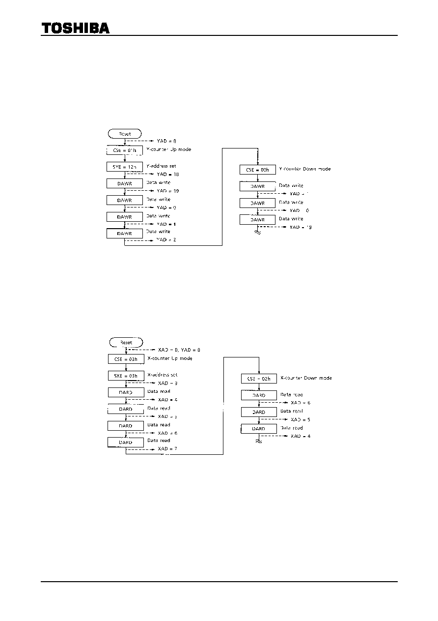
T6K11
2001-03-13 28/47
Fig. 11 shows a typical operation of the Y (page) -address counter.
After a reset, the Y (page) -address (YAD) is set to 0 and the Y (page) -counter / Up mode is selected by the
command CSE. Then when data is read or written to the display RAM, the Y (page) -address counter is
incremented. When data is read or written at YAD = 19, the Y (page) -address is recycled to 0. Similarly, if
the Y (page) Down mode is selected by the command CSE, the Y (page) -address is automatically
decremented as the counter continues counting down. When data is read or written at YAD = 0, the Y (page)
-address is recycled to 19. In the example here, the Y (page) -address counter is selected by CSE, so the
X-address counter does not count.
Fig. 11
Data read
When executing Data Read, the T6K11 directly accesses the display RAM addresses to read out data.
Therefore, when the Data Read command is executed after setting the X and Y addresses, data is output
immediately from the display RAM.
Fig. 12
T6K11
2001-03-13 29/47
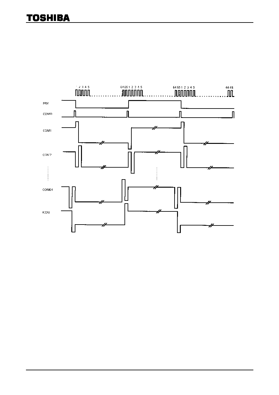
FRS control
The T6K11 has a command FRS that allows you to choose a number of lines at which the alternating signal
(FR) is inverted every time. The T6K11's alternating signal can be inverted in the range of two lines up to
the same number of lines as the duty cycle. Normally, 00H may be selected for the FRS command, so that
the FR signal is inverted when the same number of lines as the duty cycle are latched every time. To obtain
better display quality, FRS need to be adjusted to match the characteristics of each type of LCD panel used.
(a) For 1 / 65 duty and FRS = 00H (inverted at 64 + 1 lines)
Fig. 13

T6K11
2001-03-13 30/47
(b) For 1 / 35 and FRS = 10H (inverted at 16 + 1 lines)
Fig. 14

T6K11
2001-03-13 31/47
Standby function
The T6K11 has a /STB pin. When input to this pin is pulled low, the T6K11 enters a standby state. In this
state, the CR circuit clock driver is deactivated and the device is placed in a Low Power mode to suppress
current consumption. Even when the T6K11 is in standby state (the CR circuit is deactivated, so is the LCD
display clock), it can be communicated from the MPU. Since data read/write operations are possible while
the display is turned off, this helps to reduce current consumption.
In standby state, all of the LCD drive power supply pins VLC0 to VLC5 are tied to the V
SS
level.
When the standby function is used, the data in the display RAM is the display data that has been stored in
it before the standby function is turned on.
Function Oscillator
LCD Drive Power
Supply
LCD Drive Output
Normal
state
Operable Operable Operable
Standby state
Deactivated
Fixed to V
SS
level
Fixed to V
SS
level
Reset function
The T6K11 has a / RST pin. When input to this pin is pulled low, the T6K11 is reset, with its internal circuits
(register contents) initialized as shown below.
(1) Display direction ............... CDR = 1, SDR = 1
(2) Display mode ................... Normal display mode
(3) Display ............................. Turned OFF
(4) Counter ............................ Y-counter, Up mode
(5) Analog control .................. CDA = 0, DC = 0
(6) Bias .................................. 1/9 bias
(7) Duty cycle ........................ 1/65 duty
(8) Alternating signal (FR) ....... FRS = 00H
(FR inverted at the same number of lines as the duty cycle)
(9) Contrast ........................... 00H (lightest)
The T6K11 does not have a facility to reset the display RAM (to clear the data in it). In the initial state
(immediately after power-ON), the display RAM contains indeterminate data which are either high or low.
Therefore, Toshiba recommends using the Data Write command to execute a display clearing sequence
before reading or writing to the display RAM.
T6K11
2001-03-13 32/47
Oscillation frequency
The T6K11 contains a CR oscillator. The T6K11's frame frequency (f
FR
) is derived from the CR circuit's
oscillation frequency (f
osc
) by diving it an appropriate value. The relationship between the oscillation
frequency (f
osc
) and the frame frequency (f
FR
) is shown below.
Duty Cycle
FRS
Selection
Oscillation
Frequency
(f
osc
)
CL
Frequency
f
FR
Frequency
1 / 65duty
Inverted at
duty
41 kHz
8
OSC
f
65
8
OSC
f
¥
1 / 57duty
Inverted at
duty
41 kHz
10
OSC
f
57
10
OSC
f
¥
1 / 49duty
Inverted at
duty
41 kHz
12
OSC
f
49
12
OSC
f
¥
1 / 35duty
Inverted at
duty
41 kHz
16
OSC
f
35
16
OSC
f
¥
1 / 65duty
Inverted at
17 lines
41 kHz
8
OSC
f
17
8
OSC
f
¥
1 / 2duty
Inverted at
2 lines
41 kHz
256
OSC
f
2
256
OSC
f
¥
Note: The T6K11 has its f
FR
frequency varied by the FRS setup data. Therefore, consider the relationship
between the duty cycle and the number of inversion lines when you adjust the f
FR
frequency to suit he CD
panel used.
The relationship between bias control and contrast control
The contrast adjustment range of VLC0 is varied according to the BIAS that is set in the R2 register and
VLC0 CONTROL that is set in the R6 register.
So, it is necessary to control these registers when you adjust the VLC0 output voltage to suit the LCD panel
used.
The relationship between the BIAS and the VLC0 output voltage is shown below.
R6: VLC0 control
VLC0 output voltage (V)
Display mode
DB7
DB6
1/6 bias
1/7 bias
1/8 bias
1/9 bias
1 1
9.33 10.89 12.45 14.00
1
0
8.67 10.11 11.55 13.00
0 1
8.00 9.33 10.67 12.00
N/F = 1
0
0
7.34 8.56 9.78 11.00
1
1
3.33 3.89 4.55 5.00
1
0
3.25 3.79 4.33 4.87
0
1
3.15 3.67 4.20 4.72
N/F = 0
0
0
3.04 3.55 4.05 1.56
(Note): The V
LC0
output voltage values are typical values at max contrast.
T6K11
2001-03-13 33/47
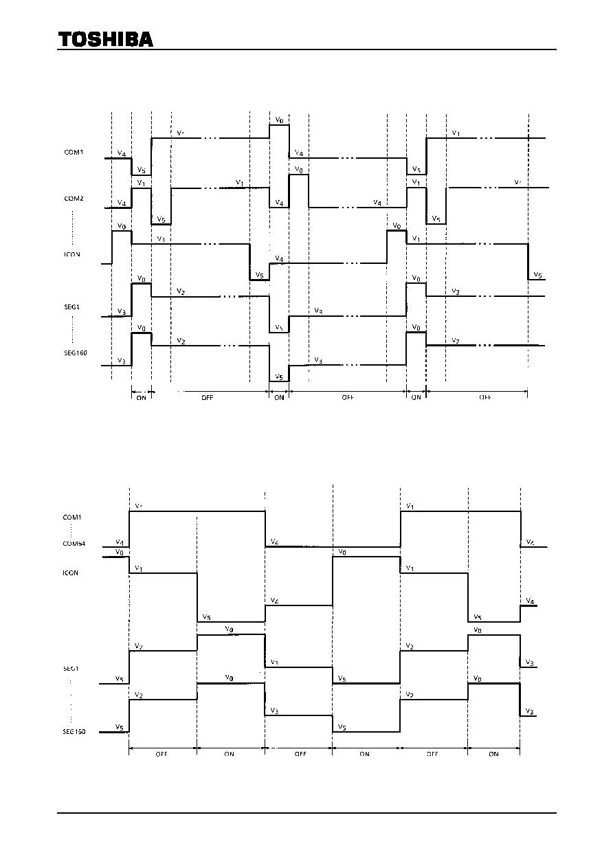
LCD drive waveform
(a) For normal display mode where duty cycle = 1/65 and FRS = 00h
Fig. 15
(b) For power save mode where duty cycle = 1/2
Fig. 16

T6K11
2001-03-13 34/47
Maximum Ratings
(Referenced to
V
SS
= 0 V, Ta = 25∞C unless otherwise noted)
Characteristics Symbol
Rating
Unit
Remark
Power Supply Voltage (1)
DV
DD
, AV
DD
-0.3~V
SS
+ 7.0
V
(Note 1)
Power Supply Voltage (2)
(Note 2)
-0.3~V
SS
+ 18.0
V
(Note 1), (Note 3)
Input Voltage (1)
V
INA
-0.3~AV
DD
+ 0.3
V
(Note 1), (Note 4)
Input Voltage (2)
V
IND
-0.3~DV
DD
+ 0.3
V
(Note 1), (Note 4)
Output Voltage (1)
V
OA
-0.3~V
SS
+ 18.0
V
(Note 1)
Output Voltage (2)
V
OD
-0.3~DV
DD
+ 0.3
V
(Note 1)
Operating Temperature
T
opr
-25~75 ∞C
Storage Temperature
T
stg
-40~125 ∞C
Note 1: These values are referenced to AV
SS
= DV
DD
= 0 V.
Note 2: V
CC
, VLC0, VLC1, VLC2, VLC3, VLC4, VLC5
Note 3: The condition V
CC
VLC0 VLC1 VLC2 VLC3 VLC4 VLC5 must always be met.
Note 4: The condition AV
DD
DV
DD
must always be met.
Note 5: If the device is used exceeding its absolute maximum ratings, the device may not only break down but also
loose reliability and malfunction. Therefore, Toshiba recommends that for normal operation, the device be
used within the range of electrical characteristics shown in the next page.
T6K11
2001-03-13 35/47
Electrical Characteristics
DC Characteristics (1)
referenced to DV
DD
= 3.0 V, AV
DD
= 3.0 V, V
SS
= 0 V, V
CC
= 15.0 V,
V
LC0
= 14.0 V, Ta = -20
to 60∞C unless otherwise noted
Characteristics Symbol
Test
Circuit
Test Condition
Min
Typ.
Max
Unit
Relevant Pin
Operating Voltage (1)
AV
DD
DV
DD
3.0 5.5 V AV
DD
Operating Voltage (2)
DV
DD
1.8
3.0
3.3
V
DV
DD
Operating Voltage (3)
V
CC
VCL0
6.0 -
V
SS
16.5 -
V
SS
V V
CC
, VCL0
High
Level
V
IH
0.80 ◊
DV
DD
DV
DD
V
Input
Voltage
Low
Level
V
IL
0
0.20 ◊
DV
DD
V
(Note 1)
High
Level
V
OH
I
OH
= -400 µA
DV
DD
- 0.2
DV
DD
V
Output
Voltage
Low
Level
V
OL
I
OL
= 400 µA
0
0.2 V
DB0 to DB7
Normal
Mode
Rcol1
(Note
2)
7.5 k
Segment
Driver ON-
Resistance
Power
Save
Mode
Rcol2
(Note
3)
15.0 k
SEG1 to
SEG160
Normal
Mode
Rrow1
(Note
2)
1.5 k
Common
Driver ON-
Resistance
Power
Save
Mode
Rrow2
(Note
3)
5.0 k
COM1 to
COM64
ICON
Input Leakage
Current
I
IL
V
IND
= DV
DD
to GND
-1
1 µA (Note
1)
Output Leakage
Current
I
OL
V
OD
= DV
DD
to GND
-1
1
µA
DB0 to DB7
Note 1: This applies to pins DB0 through DB7, RS, /WR, /RD, /CS1, CS2, /RST, /STB, P/S, 68/80, and CLS.
Note 2: Referenced to AV
DD
= 3.0 V, DV
DD
= 3.0 V, VLC0 = 11.0 V, V
CC
= 16.5 V, 1/9 bias, current load
Iload = 100 µA, Ta = 25∞C.
Note 3: Referenced to AV
DD
= 3.0 V, DV
DD
= 3.0 V, VLC0 = 4.0 V, V
CC
= 6.0 V, 1/9 bias, current load
Iload = 100 µA, Ta = 25∞C.

T6K11
2001-03-13 36/47
DC Characteristics (2)
referenced to DV
DD
= 3.0 V, AV
DD
= 3.0 V, V
SS
= 0 V, V
CC
= 15.0 V,
V
LC0
= 14.0 V, Ta = -20
to 60∞C unless otherwise noted
Characteristics Symbol
Test
Circuit
Test Condition
Min
Typ.
Max
Unit
Relevant Pin
Operating Frequency
(Input Frequency)
CLIN
41 kHz
CL
Output Frequency
CLO
39 41 43 kHz
CL
External Clock
Frequency
Fex
39 41 43 kHz
CL
External Clock Duty
Cycle
Fduty
45 50 55 %
CL
External Clock Rise /
Fall Time
Tr / Tf
10 ns
CL
DC Characteristics (3)
referenced to DV
DD
= 3.0 V, AV
DD
= 3.0 V, V
SS
= 0 V, Ta = -20
to 60∞C
unless otherwise noted
Characteristics Symbol
Test
Circuit
Test Condition
Min
Typ.
Max
Unit
Relevant Pin
Output Voltage
Characteristic
(Using ◊2 Step-up
Circuit)
V
O1
(1) (Note
4)
5.50
5.60
V
VOUT1
Output Voltage
Characteristic
(Using ◊3 Step-up
Circuit)
V
O2
(2) (Note
5)
8.33
8.55
V
VOUT2
Output Voltage
Characteristic
(Using ◊4 Step-up
Circuit)
V
O3
(3) (Note
6) 11.25
11.50
V
VOUT3
Output Voltage
Characteristic
(Using ◊5 Step-up
Circuit)
V
O4
(4) (Note
7) 14.15
14.40
V
VOUT4
Note 4: Referenced to DV
DD
= AV
DD
= 3.0 V, Iload = 200 µA, V
CC
= 6.0 V (supplied from external source), CnA -
CnB = 1.0 µF, VOUTn - V
SS
= 1.0 µF, CL = 41.0 kHz.
Note 5: Referenced to DV
DD
= AV
DD
= 3.0 V, Iload = 200 µA, V
CC
= 9.0 V (supplied from external source), CnA -
CnB = 1.0 µF, VOUTn - V
SS
= 1.0 µF, CL = 41.0 kHz.
Note 6: Referenced to DV
DD
= AV
DD
= 3.0 V, Iload = 200 µA, V
CC
= 12.0V (supplied from external source), CnA -
CnB = 1.0 µF, VOUTn - V
SS
= 1.0 µF, CL = 41.0 kHz.
Note 7: Referenced to DV
DD
= AV
DD
= 3.0 V, Iload = 200 µA, V
CC
= 15.0 V (supplied from external source), CnA -
CnB = 1.0 µF, VOUTn - V
SS
= 1.0 µF, CL = 41.0 kHz.

T6K11
2001-03-13 37/47
DC Characteristics (4)
referenced to DV
DD
=
3.0 V, AV
DD
=
3.0 V, V
SS
=
0 V,
Ta = -20
to 60∞C unless otherwise noted
Characteristics Symbol
Test
Circuit
Test Condition
Min
Typ.
Max
Unit
Relevant Pin
Current Consumption
(1)
ISS1
(Note
8)
235
315 µA
V
SS
Current Consumption
(2)
ISS1
(Note
9)
250
360 µA
V
SS
Current Consumption
(3)
ISS3
(Note
10)
470
500 µA
V
SS
Current Consumption
(4)
ISS4
(Note
11)
40 45 µA
V
SS
Current Consumption
(5)
ISSSTB
(Note
12)
1 µA
V
SS
Note 8: Referenced to AV
DD
= DV
DD
= 3.0 V, AV
SS
= DV
SS
= 0 V, V
CC
= VOUT4 (using ◊ 5 step-up), internal CR
oscillator turned on (CL = 41 kHz), 1/9 bias, 1/65 duty, D/A converter turned on, LCD nonloaded, display
pattern: all "white," no data access, normal display mode, contrast control: R5 = BFH, VLC0 = 13.0 V,
Ta = 25∞C, FRS = 0H.
Note 9: Referenced to AV
DD
= DV
DD
= 3.0 V, AV
SS
= DV
SS
= 0 V, V
CC
= VOUT4 (using ◊ 5 step-up), internal CR
oscillator turned on (CL = 41 kHz), 1/9 bias, 1/65 duty, D/A converter turned on, LCD nonloaded, display
pattern: "checker," no data access, normal display mode, contrast control: R5 = BFH, VLC0 = 13.0 V,
Ta = 25∞C, FRS = 0H.
Note 10: Referenced to AV
DD
= DV
DD
= 3.0 V, AV
SS
= DV
SS
= 0 V, V
CC
= VOUT4 (using ◊ 5 step-up), internal CR
oscillator turned on (CL = 41 kHz), 1/9 bias, 1/65 duty, D/A converter turned on, LCD nonloaded, display
pattern: "checker," data access performed ( /CE = 1 MHz), normal display mode, contrast control: R5 = BFH,
VLC0 = 13.0 V, Ta = 25∞C, FRS = 0H.
Note 11: Referenced to AV
DD
= DV
DD
= 3.0 V, AV
SS
= DV
SS
= 0 V, V
CC
= VOUT4 (using ◊ 5 step-up), internal CR
oscillator turned on (CL = 41 kHz), 1/9 bias, 1/2 duty, D/A converter turned on, LCD nonloaded, display
pattern: "checker," no data access, power save mode.
Note 12: Referenced to AV
DD
= DV
DD
= 3.0 V, AV
SS
= DV
SS
= 0 V, V
CC
= 16.5 V, LCD nonloaded, no data access.
DC Characteristics (5)
referenced to DV
DD
=
3.0 V, AV
DD
=
3.0 V, V
SS
=
0 V, Ta = 25∞C
unless otherwise noted
Characteristics Symbol
Test
Circuit
Test Condition
Min
Typ.
Max
Unit
Relevant Pin
Ta = 25∞C
(Note 13)
13.8
14.0
14.2
V
VLC0
Ta = 25∞C
(Note 14)
12.8
13.0
13.2
V
VLC0
Ta = 25∞C
(Note 15)
11.8
12.0
12.2
V
VLC0
VLC0 Output Voltage
V0out
Ta = 25∞C
(Note 16)
10.8
11.0
11.2
V
VLC0
VLC0 Output Voltage
Inclination
V0INC
Ta
=
-20 to 60∞C
(Note 13)
-0.05
V0out
0.05 %/∞C
VLC0
Note 13: AV
DD
= DV
DD
= 3.0 V, AV
SS
= DV
SS
= 0 V, 1/65 duty, 1/9 bias, V
CC
= 15.0 V (supplied from external
source), CONTRAST CONTROL (R5) = FFh, D/A converter turned on, LCD nonloaded, normal display
mode.
Note 14: AV
DD
= DV
DD
= 3.0 V, AV
SS
= DV
SS
= 0 V, 1/65 duty, 1/9 bias, V
CC
= 14.0 V (supplied from external
source), CONTRAST CONTROL (R5) = BFh, D/A converter turned on, LCD nonloaded, normal display
mode.
Note 15: AV
DD
= DV
DD
= 3.0 V, AV
SS
= DV
SS
= 0 V, 1/65 duty, 1/9 bias, V
CC
= 13.0 V (supplied from external
source), CONTRAST CONTROL (R5) = 7Fh, D/A converter turned on, LCD nonloaded, normal display
mode.
Note 16: AV
DD
= DV
DD
= 3.0 V, AV
SS
= DV
SS
= 0 V, 1/65 duty, 1/9 bias, V
CC
= 12.0 V (supplied from external
source), CONTRAST CONTROL (R5) = 3Fh, D/A converter turned on, LCD nonloaded, normal display
mode.

T6K11
2001-03-13 38/47
DC Characteristics (6)
referenced to DV
DD
=
3.0 V, AV
DD
=
3.0 V, V
SS
=
0 V,
Ta = -20
to 60∞C unless otherwise noted
Characteristics Symbol
Test
Circuit
Test Condition
Min
Typ.
Max
Unit
Relevant Pin
Vopoff1
(Note 17, 21, 22)
-200
200 mV (Note
20)
D/A Converter Output
Voltage Offset (1)
Vopoff2
(Note 18, 21, 22)
-200
200 mV (Note
20)
Voffset1
I
Load
= ±20 µA
±50
±80 mV
VLC0, VLC2,
VLC3
D/A Converter Output
Voltage Offset (2)
Voffset2
I
Load
= ±3 µA
±30
±50 mV
VLC1,
VLC4
D/A Converter Output
Voltage Offset (3)
Vopoffs
(Note 19, 21, 22)
-200
200 mV (Note
20)
Note 17: Referenced to AV
DD
= DV
DD
= 3.0 V, AV
SS
= DV
SS
= 0 V, 1/65 duty, 1/9 bias, V
CC
= 15.0 V (supplied from
external source), contrast control = Max, D/A converter: ON, step-up circuit: OFF, LCD nonloaded, normal
display mode.
VLC0 pin: 14.0 - VLC0 = Vopoff1
VLC1 pin: (VLC0 ◊ 8/9) - VLC1 = Vopoff1
VLC2 pin: (VLC0 ◊ 7/9) - VLC2 = Vopoff1
VLC3 pin: (VLC0 ◊ 2/9) - VLC3 = Vopoff1
VLC4 pin: (VLC0 ◊ 1/9) - VLC4 = Vopoff1
Note 18: Referenced to AV
DD
= DV
DD
= 3.0 V, AV
SS
= DV
SS
= 0 V, 1/2 duty, 1/9 bias, V
CC
= 6.0 V (supplied from
external source), contrast control = Max, D/A converter: ON, step-up circuit: OFF, LCD nonloaded, power
save mode.
VLC0 pin: 5.0 - VLC0 = Vopoff2
VLC1 pin: (VLC0 ◊ 8/9) - VLC1 = Vopoff2
VLC2 pin: (VLC0 ◊ 7/9) - VLC2 = Vopoff2
VLC3 pin: (VLC0 ◊ 2/9) - VLC3 = Vopoff2
VLC4 pin: (VLC0 ◊ 1/9) - VLC4 = Vopoff2
Note 19: Referenced to AV
DD
= DV
DD
= 3.0 V, AV
SS
= DV
SS
= 0 V, 1/65 duty, 1/9 bias, V
CC
= 15.0 V (supplied from
external source), contrast control = Max, D/A converter: ON, step-up circuit: OFF, LCD nonloaded, normal
display mode.
Vopoffs = ((VLC1 - VLC2) - (VLC0 - VLC1)) + ((VLC3 - VLC4) - (VLC4 - VLC5))
Note 20: VLC0, VLC1, VLC2, VLC3 and VLC4.
Note 21: VLC0, VLC2, VLC3: I
Load
= ±30 µA
Note 22: VLC1,VLC4: I
Load
= ±3 µA
T6K11
2001-03-13 39/47
Test Circuits
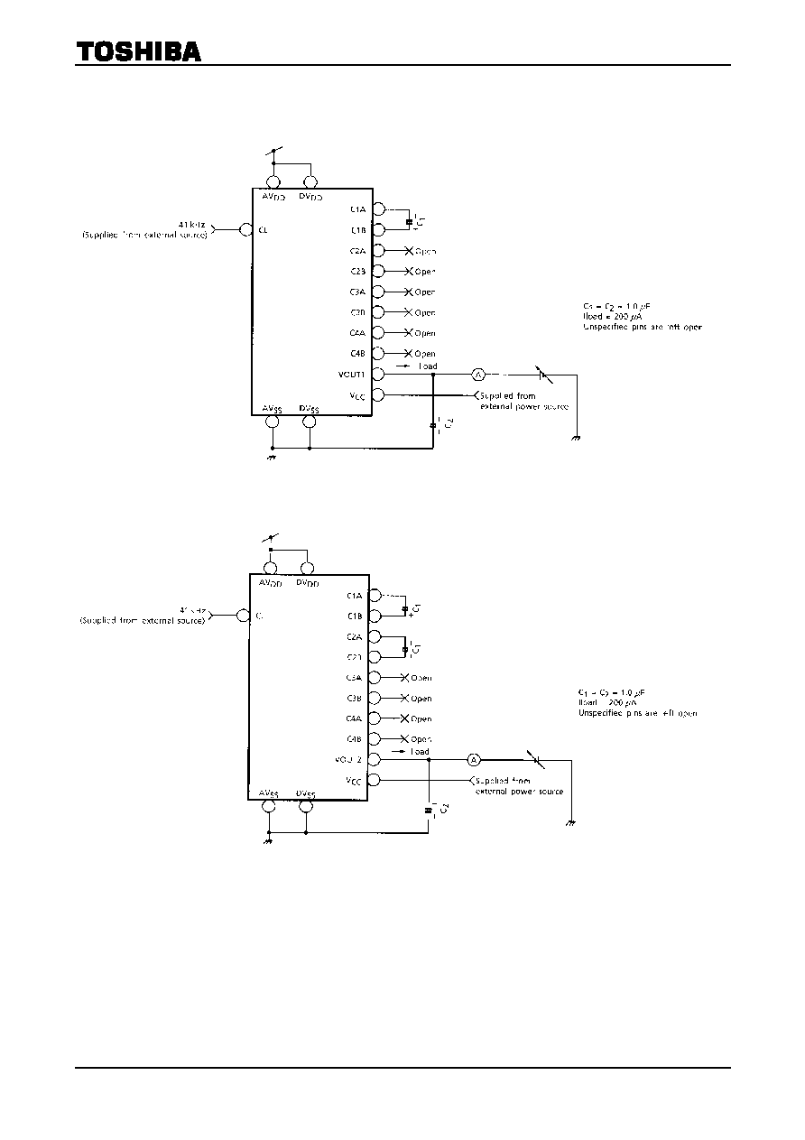
(1) Test circuit for cases when ◊2 step-up circuit is used
(2) Test circuit for cases when ◊3 step-up circuit is used

T6K11
2001-03-13 40/47
(3) Test circuit for cases when ◊4 step-up circuit is used
(4) Test circuit for cases when ◊5 step-up circuit is used

T6K11
2001-03-13 41/47
AC Characteristics
(1)
80-series parallel interface read / write characteristics
Test Condition
Referenced to V
SS
= 0 V, DV
DD
= AV
DD
= 2.4 to 2.7 V,
V
CC
= AV
DD
, Ta = -20 to 60∞C unless otherwise noted
Characteristics Symbol
Min
Max
Unit
Enable Cycle Time
t
cycE
1000
ns
Enable Pulse Width
PWEL
500
ns
Enable Rise / Fall Time
t
Er
, t
Ef
20 ns
Address Setup Time
t
AS
25
ns
Address Hold Time
t
AH
25
ns
Data Setup Time
t
DS
130
ns
Write Data Hold Time
t
DHW
70
ns
Data Delay Time
t
DD
400
ns
Read Data Hold Time
t
DHR
50
ns
T6K11
2001-03-13 42/47
Referenced
to
V
SS
= 0 V, DV
DD
= AV
DD
= 2.7 to 3.3 V,
V
CC
= AV
DD
, Ta = -20 to 60∞C unless otherwise noted
Characteristics Symbol
Min
Max
Unit
Enable Cycle Time
t
cycE
500
ns
Enable Pulse Width
PWEL
300
ns
Enable Rise/Fall Time
t
Er
, t
Ef
15 ns
Address Setup Time
t
AS
20
ns
Address Hold Time
t
AH
20
ns
Data Setup Time
t
DS
60
ns
Write Data Hold Time
t
DHW
50
ns
Data Delay Time
t
DD
200
ns
Read Data Hold Time
t
DHR
20
ns

T6K11
2001-03-13 43/47
AC Characteristics
(2)
68-series parallel interface read / write characteristics
Test Condition
Referenced to V
SS
= 0 V, DV
DD
= AV
DD
= 2.4 to 2.7 V,
V
CC
= AV
DD
, Ta = -20 to 60∞C unless otherwise noted
Characteristics Symbol
Min
Max
Unit
Enable Cycle Time
t
cycE
1000
ns
Enable Pulse Width
PWEL
500
ns
Enable Rise / Fall Time
t
Er
, t
Ef
20 ns
Address Setup Time
t
AS
25
ns
Address Hold Time
t
AH
25
ns
Data Setup Time
t
DS
130
ns
Write Data Hold Time
t
DHW
70
ns
Data Delay Time
t
DD
400
ns
Read Data Hold Time
t
DHR
50
ns

T6K11
2001-03-13 44/47
Referenced to V
SS
= 0 V, V
DD
= 2.7 to 3.3 V, V
CC
= AV
DD
,
Ta
=
-20 to 60∞C unless otherwise noted
Characteristics Symbol
Min
Max
Unit
Enable Cycle Time
t
cycE
500
ns
Enable Pulse Width
PWEL
300
ns
Enable Rise/Fall Time
t
Er
, t
Ef
15 ns
Address Setup Time
t
AS
20
ns
Address Hold Time
t
AH
20
ns
Data Setup Time
t
DS
60
ns
Write Data Hold Time
t
DHW
50
ns
Data Delay Time
t
DD
200
ns
Read Data Hold Time
t
DHR
20
ns

T6K11
2001-03-13 45/47
AC Characteristics
(3)
Serial interface read / write characteristics
Test Condition
Referenced to V
SS
= 0 V, DV
DD
= AV
DD
= 2.4 to 2.7 V,
V
CC
= AV
DD
, Ta = -20 to 60∞C unless otherwise noted
Characteristics Symbol
Min
Max
Unit
Clock Cycle Time
t
cycC
1000
ns
Clock Pulse Width
PWCL, PWCH
500
ns
Clock Rise/Fall Time
t
Cr
, t
Cf
20 ns
CS Setup Time
t
CSS
300
ns
CS Hold Time
t
CSH
300
ns
Address Setup Time
t
AS
300
ns
Address Hold Time
t
AH
300
ns
Data Setup Time
t
DS
250
ns
Data Hold Time
t
DH
250
ns

T6K11
2001-03-13 46/47
Referenced to V
SS
= 0 V, DV
DD
= AV
DD
= 2.7 to 3.3 V,
V
CC
= AV
DD
, Ta = -20 to 60∞C unless otherwise noted
Characteristics Symbol
Min
Max
Unit
Clock Cycle Time
t
cycC
400
ns
Clock Pulse Width
PWCL, PWCH
150
ns
Clock Rise/Fall Time
t
Cr
, t
Cf
15 ns
CS Setup Time
t
CSS
250
ns
CS Hold Time
t
CSH
250
ns
Address Setup Time
t
AS
250
ns
Address Hold Time
t
AH
250
ns
Data Setup Time
t
DS
150
ns
Data Hold Time
t
DH
150
ns
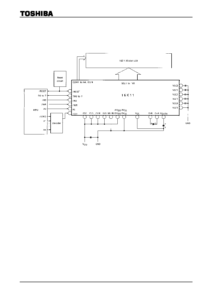
T6K11
2001-03-13 47/47
Example of Application Circuit
T6K11
Internal CR oscillator used
◊5
step-up circuit used
8-bit parallel MPU interface used