 | –≠–ª–µ–∫—Ç—Ä–æ–Ω–Ω—ã–π –∫–æ–º–ø–æ–Ω–µ–Ω—Ç: TA1218F | –°–∫–∞—á–∞—Ç—å:  PDF PDF  ZIP ZIP |

TA1218N/F
2000-09-11 1/40
TOSHIBA Bipolar Linear Integrated Circuit Silicon Monolithic
TA1218N, TA1218F
Audio/Video Switching IC for TVs
The TA1218N/F is an audio/video switching IC for TV sets.
Conforming to I
2
C bus standards, it allows you to perform
various switching operations through the bus lines by using a
microcomputer. Thanks to its 2-channel outputs, the TA1218N/F
can also be used for the PIP systems. Furthermore, since the
presence of a signal on its sync signal output pin can be
determined by a microcomputer, it is possible to check each
input/output channel (self-diagnosis).
This IC has the same pin assignments as the TA1219AN
(SDIP36), a 1-channel output version of the TA1218N/F, so
these chips are pin compatible on pins 3 to 20 and 23 to 40.
Features
∑ I
2
C bus control
∑ Video : 5-channel inputs and 2-channel outputs
(2 channels conforming to S system)
∑ Audio : 5-channel inputs and 3-channel outputs
∑ Self-diagnostic function
∑ ADC inputs based on European 21-pin standards
∑ Switchable subaddress
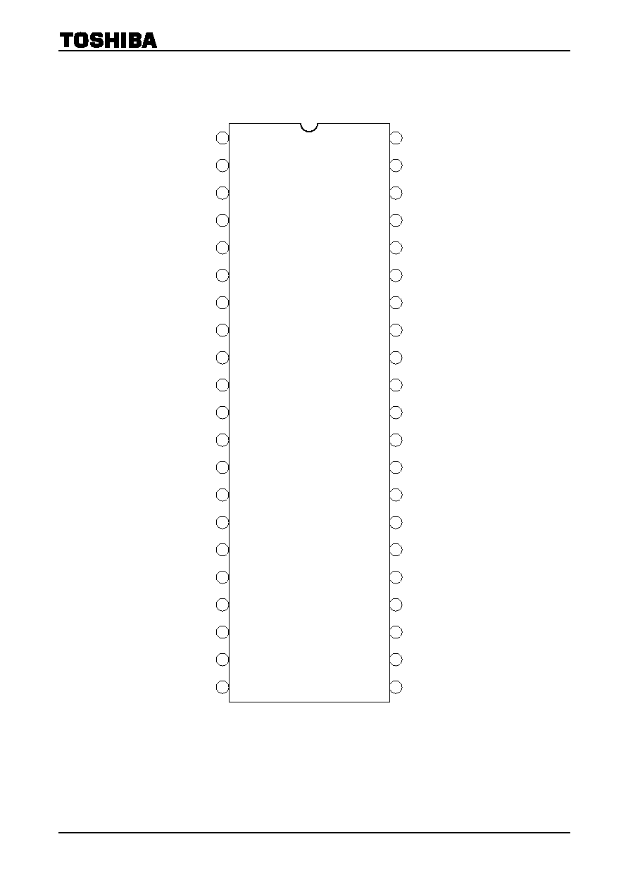
TA1218N
TA1218F
Weight
SDIP42-P-600-1.78 : 4.13 g (typ.)
QFP48-P-1014-0.80 : 0.83 g (typ.)
∑ TOSHIBA is continually working to improve the quality and reliability of its products. Nevertheless, semiconductor devices in general
can malfunction or fail due to their inherent electrical sensitivity and vulnerability to physical stress. It is the responsibility of the
buyer, when utilizing TOSHIBA products, to comply with the standards of safety in making a safe design for the entire system, and
to avoid situations in which a malfunction or failure of such TOSHIBA products could cause loss of human life, bodily injury or
damage to property.
In developing your designs, please ensure that TOSHIBA products are used within specified operating ranges as set forth in the
most recent TOSHIBA products specifications. Also, please keep in mind the precautions and conditions set forth in the "Handling
Guide for Semiconductor Devices," or "TOSHIBA Semiconductor Reliability Handbook" etc..
∑ The TOSHIBA products listed in this document are intended for usage in general electronics applications (computer, personal
equipment, office equipment, measuring equipment, industrial robotics, domestic appliances, etc.). These TOSHIBA products are
neither intended nor warranted for usage in equipment that requires extraordinarily high quality and/or reliability or a malfunction or
failure of which may cause loss of human life or bodily injury ("Unintended Usage"). Unintended Usage include atomic energy
control instruments, airplane or spaceship instruments, transportation instruments, traffic signal instruments, combustion control
instruments, medical instruments, all types of safety devices, etc.. Unintended Usage of TOSHIBA products listed in this document
shall be made at the customer's own risk.
∑ The products described in this document are subject to the foreign exchange and foreign trade laws.
∑ The information contained herein is presented only as a guide for the applications of our products. No responsibility is assumed by
TOSHIBA CORPORATION for any infringements of intellectual property or other rights of the third parties which may result from its
use. No license is granted by implication or otherwise under any intellectual property or other rights of TOSHIBA CORPORATION or
others.
∑ The information contained herein is subject to change without notice.
000707EBA1

TA1218N/F
2000-09-11 2/40
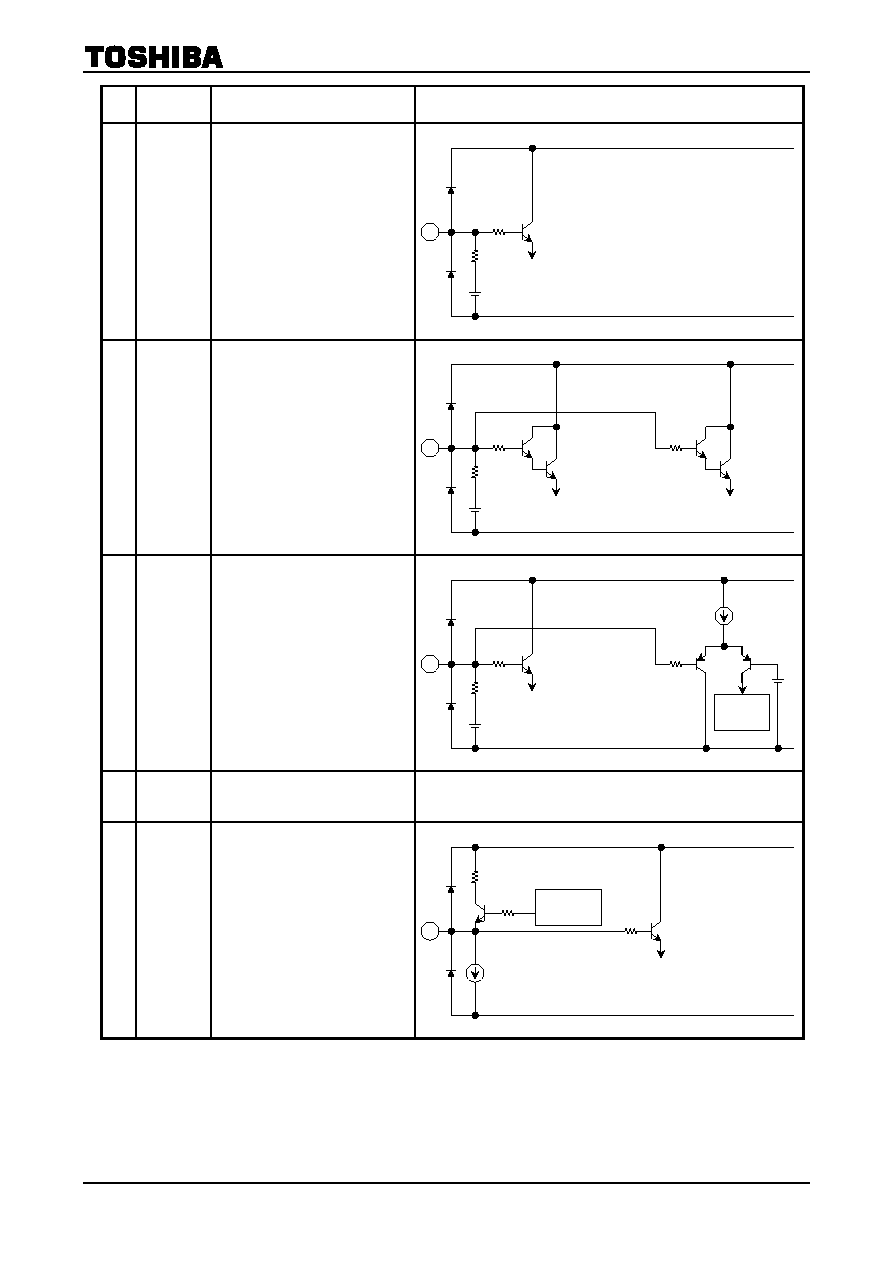
Block Diagram
Note1: ( ): The terminal number of TA1218F.
(6)
Det Select
Det in
V
in
V1
V
in
V2
V
in
TV
Y/V
in
S1
Y/V
in
S2
C
in
S1
C
in
S2
Sync out
L
in
S1
L
in
S2
L
in
V1
L
in
V2
L
in
TV
R
in
S1
R
in
S2
R
in
V1
R
in
V2
R
in
TV
V
CC
GND
V
CC
GND
V
out
1
V
out
2
Y
out
Y
in
C
out
C
in
SCL
SDA
Address
I/O1 (3 level)
I/O2 (3 level)
I/O3
O4
O5
L
out
TV
L
out
1
L
out
2
R
out
TV
R
out
1
R
out
2
4
3
33
23
-6dB
10
28
7
12
16
S
S
18
24
25
27
19
20
21
22
41
+
+
14
11
15
8
29
5
26
Pulse
conver-
ter
13
17
9
31
6
1
37
40
39
35
2
38
42
36
30
34
32
Sync
separator
(46)
(45)
(26)
(2)
(8)
(12)
(10)
(15)
(24)
(7)
(11)
(3)
(31)
(47)
(9)
(13)
(5)
(29)
(48)
(33)
(21)
(38)
(42)
(36)
(32)
(34)
(30)
(22)
(23)
(25)
(16)
(17)
(18)
(19)
(41)
(40)
(37)
(43)
(39)
(35)
(44)
24
I
2
L
Logic
I
2
C
bus
I/O
Mute
TA1218N/F
2000-09-11 3/40
Pin Assignment
TA1218N
L
ou
t
2
R
out
2
Det in
Det Select
L
in
TV
R
in
TV
V
in
TV
L
in
V1
R
in
V1
V
in
V1
L
in
S1
Y/V
in
S1
R
in
S1
C
in
S1
L
in
S2
Y/V
in
S2
R
in
S2
C
in
S2
I/O1
I/O2
I/O3
V
out
2
O5
L
out
TV
R
out
TV
V
out
1
L
out
1
Y
out
R
out
1
C
out
V
CC
C
in
R
in
V2
Y
in
L
in
V2
V
in
V2
Address
Sync out
SDA
SCL
GND
O4
4
1
2
3
5
9
6
7
8
10
14
11
12
13
15
20
17
18
19
21
16
39
42
41
40
38
34
37
36
35
33
29
32
31
30
28
23
26
25
24
22
27
11
TA1218N

TA1218N/F
2000-09-11 4/40
TA1218F
NC
V
in
TV
L
in
V1
NC
R
in
V1
V
in
V1
L
in
S1
Y/V
in
S1
R
in
S1
C
in
S1
L
in
S2
Y/V
in
S2
R
in
S2
NC
V
out
1
L
out
1
Y
out
R
out
1
C
out
V
CC
NC
NC
C
in
R
in
V2
Y
in
L
in
V2
V
in
V2
Address
4
1
2
3
5
9
6
7
8
10
14
11
12
13
15
20
17
18
19
21
16
23
24
22
38
34
37
36
35
33
29
32
31
30
28
26
25
27
C
in
S2
I/O
1
I/O
2
I/O
3
O4
NC
GND
SC
L
SD
A
S
y
nc
ou
t
39
42
41
40
43
46
45
44
48
47
R T
V
L T
V
Det
S
e
l
e
c
t
Det
i
n
R
out
2
L
out
2
V
out
2
O5
L
out
T
V
R
out
T
V
TA1218F

TA1218N/F
2000-09-11 5/40
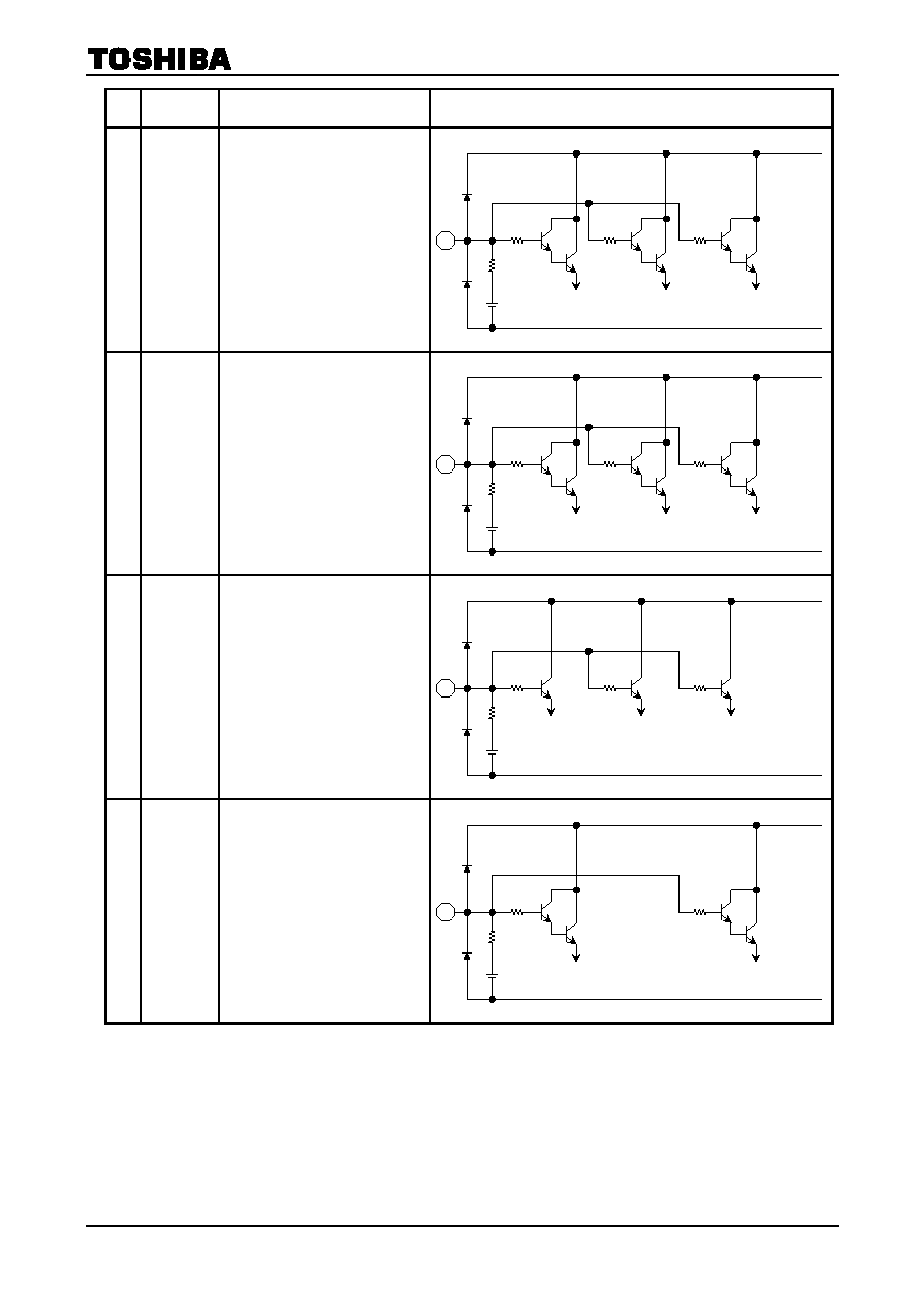
Pin Description (( ): the pin number of TA1218F)
Pin
No.
Name Function
Interface
1
(43)
L
out
2
This pin is for output a sub-channel
left audio signal. The signals fed into
the chip via L
in
V1, L
in
V2, L
in
S1,
L
in
S2, or L
in
TV is output from this
pin. The output resistance of this pin
is 45
.
Furthermore, the signal output from
this pin is pulse-converted for use in
self-diagnosis. The converted signal
is output from Sync Out.
This output can be muted in
combination with R
out
2 by bus
control.
2
(44)
R
out
2
This pin is for output a sub-channel
right audio signal. The signals fed
into the chip via R
in
V1, R
in
V2,
R
in
S1, R
in
S2, or R
in
TV is output
from this pin. The output resistance
of this pin is 45
.
Furthermore, the signal output from
this pin is pulse-converted for use in
self-diagnosis. The converted signal
is output from Sync Out.
This output can be muted in
combination with L
out
2 by bus
control.
3
(45)
Det in
This pin is for input a sync
separation signal. Input the signal
from Det Select to this pin with
capacitance coupling. The input
resistance of this pin is 18 k
.
The sync signal separated from Det
Select is outputted from Sync Out
for use in self-diagnosis.
4
(46)
Det Select
This pin is for output a sync
separation signal.
Signals V
in
V1, V
in
V2, V
in
TV,
Y/V
in
S1, V
out
1, V
out
2, Y
out
, or C
out
are outputted from this pin. The
output resistance of this pin is 35
.
Input the signal from this pin to Det
in with capacitance coupling.
70 k
20 k
1
1.
5 m
A
100
L
out
2
SW
(43)
70 k
20 k
2
1.
5 m
A
100
R
out
2
SW
(44)
<Sync out>
1 k
7
µ
A
/
1.
1
µ
A
1 k
3
7.
3 V
22.
5 k
(45)
4
100
Det Select
SW
200
(46)
TA1218N/F
2000-09-11 6/40
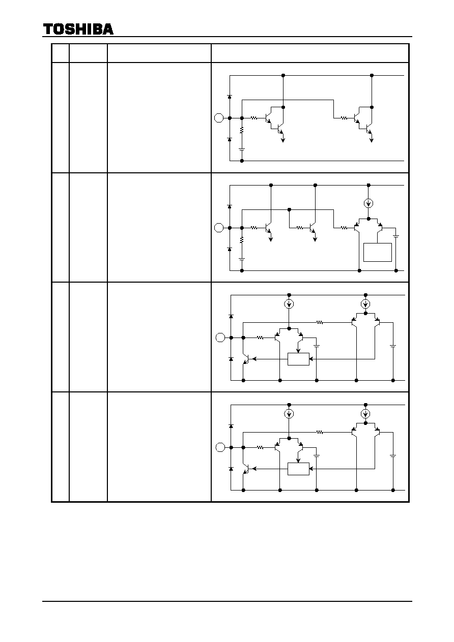
Pin
No.
Name Function
Interface
5
(47)
L
in
TV
This pin is for input a left audio
signal from the main demodulator in
the TV set. The signal fed into this
pin is presented to L
out
TV, L
out
1,
and L
out
2.
The input dynamic range of this pin
is 6.5 V
p-p
and the input resistance is
70 k
.
6
(48)
R
in
TV
This pin is for input a right audio
signal from the main demodulator in
the TV set. The signal fed into this
pin is presented to R
out
TV, R
out
1,
and R
out
2.
The input dynamic range of this pin
is 6.5 V
p-p
and the input resistance is
70 k
.
7
(2)
V
in
TV
This pin is for input a composite
audio signal from the main
demodulator in the TV set. The
signal fed into this pin is presented
to V
out
1, V
out
2, Y
out
, and C
out
. The
same signal is also output from Det
Select as a sync separation signal.
The input dynamic range of this pin
is 2.0 V
p-p
and the input resistance is
30 k
.
8
(3)
L
in
V1
This pin is for input a left audio
signal from an external source (V1
channel). This pin can also be used
for PIP signal input. The signal fed
into this pin is presented to L
out
1
and L
out
2.
The input dynamic range of this pin
is 6.5 V
p-p
and the input resistance is
70
.
<L
out
1>
70 k
1.5 k
5
5.
2 V
<L
out
2>
1.5 k
<L
out
TV>
1.5 k
(47)
<R
out
1>
70 k
1.5 k
6
5.
2 V
<R
out
2>
1.5 k
<R
out
TV>
1.5 k
(48)
<V
out
1>
<Y
out
>
<C
out
>
30 k
1.5 k
7
5.
2 V
<V
out
2>
1.5 k
<Det Select>
1.5 k
(2)
<L
out
1>
70 k
1.5 k
8
5.
2 V
<L
out
2>
1.5 k
(3)

TA1218N/F
2000-09-11 7/40
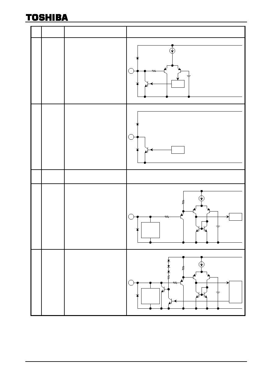
Pin
No.
Name Function
Interface
9
(5)
R
in
V1
This pin is for input a right audio
signal from an external source (V1
channel). This pin can also be used
for PIP signal input. The signal fed
into this pin is presented to R
out
1
and R
out
2.
The input dynamic range of this pin
is 6.5 V
p-p
and the input resistance is
70 k
.
10
(6)
V
in
V1
This pin is for input a composite
video signal from an external source
(V1 channel). This pin can also be
used for PIP signal input. The signal
fed into this pin is presented to
V
out
1, V
out
2, Y
out
, and C
out
. The
same signal is also output from Det
Select as a sync separation signal.
The input dynamic range of this pin
is 2.0 V
p-p
and the input resistance is
30 k
.
11
(7)
L
in
S1
This pin is for input a left audio
signal from an external source (S1
channel). The signal fed into this pin
is presented to L
out
1 and L
out
2.
The input dynamic range of this pin
is 6.5 V
p-p
and the input resistance is
70 k
.
12
(8)
Y/V
in
S1
This pin is for input a luminance
signal or composite video signal
from an external source (S1
channel). The signal fed into this pin
is presented to V
out
1, V
out
2, Y
out
,
and C
out
. The same signal is also
output from Det Select as a sync
separation signal.
The input dynamic range of this pin
is 2.0 V
p-p
and the input resistance is
30 k
.
<R
out
1>
70 k
1.5 k
9
5.
2 V
<R
out
2>
1.5 k
(5)
<V
out
1>
<Y
out
>
<C
out
>
30 k
1.5 k
10
5.
2 V
<V
out
2>
1.5 k
<Det Select>
1.5 k
(6)
<L
out
1>
70 k
1.5 k
11
5.
2 V
<L
out
2>
1.5 k
(7)
<V
out
1>
<Y
out
>
<C
out
>
30 k
1.5 k
12
5.
2 V
<V
out
2>
1.5 k
<Det Select>
1.5 k
(8)

TA1218N/F
2000-09-11 8/40
Pin
No.
Name Function
Interface
13
(9)
R
in
S1
This pin is for input a right audio
signal from an external source (S1
channel). The signal fed into this pin
is presented to R
out
1 and R
out
2.
The input dynamic range of this pin
is 6.5 V
p-p
and the input resistance is
70 k
.
14
(10)
C
in
S1
This pin is for input a chroma signal
from an external source (S1
channel). It also functions as an
S-mode select switch for the S1
channel. The S mode is selected
when the pin voltage is 2.25 V or
less. The signal fed into this pin is
presented to C
out
directly and to
V
out
1 and V
out
2 after being
combined with the Y
in
S1 signal.
The input dynamic range of this pin
is 2.0 V
p-p
and the input resistance is
30 k
.
15
(11)
L
in
S2
This pin is for input a left audio
signal from an external source (S2
channel). The signal fed into this pin
is presented to L
out
1 and L
out
2.
The input dynamic range of this pin
is 6.5 V
p-p
and the input resistance is
70 k
.
16
(12)
Y/V
in
S2
This pin is for input a luminance
signal or composite aoudio signal
from an external source (S2
channel). The signal fed into this pin
is presented to V
out
1, V
out
2, Y
out
,
and C
out
.
The input dynamic range of this pin
is 2.0 V
p-p
and the input resistance is
30 k
.
<R
out
1>
70 k
1.5 k
13
5.
2 V
<R
out
2>
1.5 k
(9)
<V
out
1>
<C
out
>
30 k
1.5 k
14
5.
2 V
<V
out
2>
1.5 k
S Mode
SW
2.
25 V
1.5 k
(10)
<L
out
1>
70 k
1.5 k
15
5.
2 V
<L
out
2>
1.5 k
(11)
<V
out
1>
<Y
out
>
<C
out
>
30 k
1.5 k
16
5.
2 V
<V
out
2>
1.5 k
(12)
TA1218N/F
2000-09-11 9/40
Pin
No.
Name Function
Interface
17
(13)
R
in
S2
This pin is for input a right audio
signal from an external source (S2
channel). The signal fed into this pin
is presented to R
out
1 and R
out
2.
The input dynamic range of this pin
is 6.5 V
p-p
and the input resistance is
70 k
.
18
(15)
C
in
S2
This pin is for input a chroma signal
from an external source (S2
channel). It also functions as an
S-mode select switch for the S2
channel. The S mode is selected
when the pin voltage is 2.25 V or
less. The signal fed into this pin is
presented to C
out
directly and to
V
out
1 and V
out
2 after being
combined with the Y
in
S2 signal.
The input dynamic range of this pin
is 2.0 V
p-p
and the input resistance is
30 k
.
19
(16)
I/O1
This is an ADC input/DAC output
pin.
The ADC is a 3-level detection type
(2 bits). The threshold levels are 7.0
V and 2.25 V.
The DAC (1 bit) is an open-collector
output. Make sure that the current
flowing into this pin is 2.0 mA or
less.
20
(17)
I/O2
This is an ADC input/DAC output
pin.
The ADC is a 3-level detection type
(2 bits). The threshold levels are 7.0
V and 2.25 V.
The DAC (1 bit) is an open-collector
output. Make sure that the current
flowing into this pin is 2.0 mA or
less.
19
7.
0 V
2.
25 V
Logic
(16)
20
7.
0 V
2.
25 V
Logic
(17)
<R
out
1>
70 k
1.5 k
17
5.
2 V
<R
out
2>
1.5 k
(13)
<V
out
1>
<C
out
>
30 k
1.5 k
18
5.
2 V
<V
out
2>
1.5 k
S Mode
SW
2.
25 V
1.5 k
(15)
TA1218N/F
2000-09-11 10/40
Pin
No.
Name Function
Interface
21
(18)
I/O3
This is an ADC input/DAC output
pin.
The ADC is a 2-level detection type
(1 bit). The threshold level is 2.25 V.
The DAC (1 bit) is an open-collector
output. Make sure that the current
flowing into this pin is 2.0 mA or
less.
22
(19)
O4
This pin is for a 1 bit DAC output.
This is an open-collector output.
Make sure that the current flowing
into this pin is 2.0 mA or less.
23
(21)
GND
This is the GND pin.
24
(22)
SCL
This pin is for input an I
2
C bus clock.
The input threshold level of this pin
is 2.25 V.
25
(23)
SDA
This is an I
2
C bus data input/output
pin. The input threshold level of this
pin is 2.25 V.
Make sure that the current flowing
into this pin is 3.0 mA or less.
21
2.
25 V
Logic
(18)
22
Logic
(19)
2.
25 V
24
Logic
Surge
protection
circuit
(22)
25
2.
25 V
Logic
Surge
protection
circuit
(25)

TA1218N/F
2000-09-11 11/40
Pin
No.
Name Function
Interface
26
(24)
Sync out
This pin is for output a
self-diagnostic sync signal. The
signal separated from V
in
TV V
in
V1,
V
in
V2, Y/V
in
S1, V
out
1, V
out
2, Y
out
,
or C
out
is outputted from this pin. In
addition, the signal derived from
L
out
1, R
out
1, L
out
2, or R
out
2 is also
output from this pin for use in audio
block diagnosis.
This is an open-collector output.
Make sure that the current flowing
into this pin is 2.0 mA or less.
27
(25)
Address
This is for an I
2
C bus slave address
select switch. The threshold level of
this pin is 2.25 V. The following lists
the addresses :
High : 92H (write), 93H (read)
Low : 90H (write), 91H (read)
28
(26)
V
in
V2
This pin is for input a composite
video signal from an external source
(V2 channel). This pin can also be
used for PIP signal input. The signal
fed into this pin is presented to
V
out
1, V
out
2, Y
out
, and C
out
. The
same signal is also output from Det
Select as a sync separation signal.
The input dynamic range of this pin
is 2.0 V
p-p
and the input resistance is
30 k
.
29
(27)
L
in
V2
This pin is for input a left audio
signal from an external source (V2
channel). This pin can also be used
for PIP signal input. The signal fed
into this pin is presented to L
out
1
and L
out
2.
The input dynamic range of this pin
is 6.5 V
p-p
and the input resistance is
70 k
.
26
1.
5 V
<Det in>
<Sound>
Output select
SW
(24)
30 k
60 k
27
Address
select SW
(25)
<V
out
1>
<Y
out
>
<C
out
>
30 k
1.5 k
28
5.
2 V
<V
out
2>
1.5 k
<Det Select>
1.5 k
(26)
<L
out
1>
70 k
1.5 k
29
5.
2 V
<L
out
2>
1.5 k
(27)
TA1218N/F
2000-09-11 12/40
Pin
No.
Name Function
Interface
30
(28)
Y
in
This pin is for input a luminance
signal from an external comb filter.
The signal fed into this pin is
presented to Y
out
.
The input dynamic range of this pin
is 5.5 V
p-p
and the input resistance is
60 k
.
31
(29)
R
in
V2
This pin is for input a right audio
signal from an external source (V2
channel). This pin can also be used
for PIP signal input. The signal fed
into this pin is presented to R
out
1
and R
out
2.
The input dynamic range of this pin
is 6.5 V
p-p
and the input resistance is
70 k
.
32
(30)
C
in
This pin is for input a chroma signal
from an external comb filter. The
signal fed into this pin is presented
to C
out
.
The input dynamic range of this pin
is 5.5 V
p-p
and the input resistance is
60 k
.
This pin also functions as a audio
mute switch. The entire audio output
can be muted by pulling the voltage
on this pin below 2.25 V.
33
(33)
V
CC
This is the power supply pin. Apply 9
V to this pin. The current
consumption of this pin is 47 mA.
34
(34)
C
out
This pin is for output a chroma
signal. The signal fed into C
in
,
C
in
S1, C
in
S2, V
in
V1, V
in
V2,
Y/V
in
S1, Y/V
in
S2, or V
in
TV is
outputted from this pin. The output
resistance of this pin is 25
.
The same signal is also outputted
from Det Select as a sync
separation signal.
<Y
out
>
60 k
1.5 k
30
5.
2 V
(28)
<R
out
1>
70 k
1.5 k
31
5.
2 V
<R
out
2>
1.5 k
(29)
<C
out
>
60 k
1.5 k
32
5.
2 V
1.5 k
Sound
Mute
2.
25 V
(30)
34
100
C
out
SW
<Det Select>
1.5 k
1.
8 m
A
(34)

TA1218N/F
2000-09-11 13/40
Pin
No.
Name Function
Interface
35
(35)
R
out
1
This pin is for output the main
channel right audio signal. The
signal fed into R
in
V1, R
in
V2, R
in
S1,
R
in
S2, or R
in
TV is outputted from
this pin. The output resistance of this
pin is 45
.
Furthermore, the signal outputted
from this pin is pulse-converted for
use in self-diagnosis. The converted
signal is outputted from Sync Out.
This outputted can be muted
independently of L
out
1 by bus
control.
36
(36)
Y
out
This pin is for output a luminance
signal. The signal fed into Y
in
,
Y/V
in
S1, Y/V
in
S2, V
in
V1, V
in
V2, or
V
in
TV is outputted from this pin. The
output resistance of this pin is 25
.
The same signal is also outputted
from Det Select as a sync
separation signal.
37
(37)
L
out
1
This pin is for output the main
channel left audio signal. The signal
fed into L
in
V1, L
in
V2, L
in
S1, L
in
S2,
or L
in
TV is outputted from this pin.
The output resistance of this pin is
45
.
Furthermore, the signal outputted
from this pin is pulse-converted for
use in self-diagnosis. The converted
signal is outputted from Sync Out.
This output can be muted
independently of R
out
1 by bus
control.
38
(38)
V
out
1
This pin is for output the main
channel composite video signal. The
signal fed into V
in
TV, V
in
V1, V
in
V2,
V
in
S1, V
in
S2, Y
in
S1
+ C
in
S1, or
Y
in
S2
+ C
in
S2 is outputted from this
pin. The output resistance of this pin
is 25
The same signal is also outputted
from Det Select as a sync
separation signal.
70 k
20 k
35
1.
5 m
A
100
R
out
1
SW
(35)
36
100
Y
out
SW
<Det Select>
1.5 k
1.
8 m
A
(36)
70 k
20 k
37
1.
5 m
A
100
L
out
1
SW
(37)
38
100
V
out
1
SW
<Det Select>
1.5 k
2.
0 m
A
(38)

TA1218N/F
2000-09-11 14/40
Pin
No.
Name Function
Interface
39
(39)
R
out
TV
This pin is for output only the signal
that is forwarded from R
in
TV. The
output resistance of this pin is 45
.
This output can be muted in
combination with L
out
TV by bus
control.
40
(40)
L
out
TV
This pin is for output only the signal
that is forwarded from L
in
TV. The
output resistance of this pin is 45
.
This output can be muted in
combination with R
out
TV by bus
control.
41
(41)
O5
This is a 1 bit DAC output pin. This
is an open-collector output. Make
sure that the current flowing into this
pin is 2.0 mA or less.
42
(42)
V
out
2
This pin is for output a sub-channel
composite video signal. The signal
fed into V
in
TV, V
in
V1, V
in
V2, V
in
S1,
V
in
S2, Y
in
S1
+ C
in
S1, or Y
in
S2
+
C
in
S2 is outputted from this pin. The
output resistance of this pin is 25
.
The same signal is also outputted
from Det Select as a sync
separation signal.
70 k
20 k
39
1.
5 m
A
100
R
out
TV
SW
(39)
(40)
70 k
20 k
40
1.
5 m
A
100
L
out
TV
SW
(41)
41
Logic
(42)
42
100
V
out
2
SW
<Det Select>
1.5 k
2.
0 m
A

TA1218N/F
2000-09-11 15/40
Bus Data Specifications
Data Structure
(1) Write
S
Slave address
(90H or 92H)
W
(0)
A Data
1 A Data
2 A Data
3 A
P
(2) Read
S
Slave address
(91H or 93H)
R
(1)
A Data
4 A
P
Note2: Slave address is switched by the voltage applied to pin 27 (address). Switched to 90H when low (GND);
switched to 92H when high (V
CC
) during write mode.
Contents of Data
Mode
Data No.
Contents of Data
B07 B06 B05 B04 B03 B02 B01 B00
Audio mute
YC output switching
Data 1
[F0H]
L
out
TV
R
out
TV
L
out
2
R
out
2
R
out
1 L
out
1
Forced TV
Audio
Y
out
C
out
B17 B16 B15 B14 B13 B12 B11 B10
Data 2
[1FH]
Sync
detection
sensitivity
switching
Sync
output
switching
Sync (diagnosis) detection switching
Input select (main)
B27 B26 B25 B24 B23 B22 B21 B20
DAC output switching
Write
Data 3
[07H]
O5 O4 I/O3
I/O2
I/O1
Input select (sub)
B37 B36 B35 B34 B33 B32 B31 B30
ADC input discrimination
S input discrimination
Read Data
4
I/O3
I/O2
Hi
I/O2
Low
I/O1
Hi
I/O1
Low
C
in
S1 C
in
S2
Power-on
reset
Note3: Shown in [ ] are reset data.
Note4: The data contents marked by a slash (/) are an unused bit (data free).
TA1218N/F
2000-09-11 16/40
Main Video Select: Terminal 38 (38) Output Signal
Bus Data
Mode Output
Signal
S Input
Discrimination
Input Select (main)
Input
S/V V
out
1
CS1 CS2 B12 B11 B10
V Y/V
in
S1 Low
S
Y/V
in
S1
+
C
in
S1
0
S1
FV Y/V
in
S1
Open
* 0 0
1
V Y/V
in
S2 Low
S
Y/V
in
S2
+
C
in
S2
0
S2
FV
(Note5)
Y/V
in
S2
*
Open
0 1
1
V1 V V
in
V1
*
* 1 0 1
V2 V V
in
V2
*
* 1 1 0
TV V V
in
TV
*
* 1 1 1
Do not use [100] for the input select data.
Note5: FV: Forced Video Mode.
Main L/R Select: Terminal 37 and 35 (37 and 35) Output Signal
Bus Data
Mode
Main L/R
Output Signal
Forced TV
Voice
Input Select (main)
Input L
out
1 R
out
1 B03
B12
B11
B10
S1 L
in
S1 R
in
S1 0
0
*
S2 L
in
S2 R
in
S2 0
1
*
V1 L
in
V1 R
in
V1 1
0
1
V2 L
in
V2 R
in
V2 1
1
0
TV L
in
TV R
in
TV
0
1 1 1
TV L
in
TV R
in
TV 1 *
*
*
Do not use [100] for the input select data.

TA1218N/F
2000-09-11 17/40
Sub (PIP) Video Select: Terminal 42 (42) Output Signal
Bus Data
Mode Output
Signal
S Input
Discrimination
Input Select (sub)
INPUT S/V
V
out2
B22
B21
B20
V Y/V
in
S1 Low
S
Y/V
in
S1
+
C
in
S1
0
S1
FV Y/VinS1
Open
* 0 0
1
V Y/V
in
S2 Low
S
Y/V
in
S2
+
C
in
S2
0
S2
FV Y/V
in
S2
*
Open
0 1
1
V1 V V
in
1
*
* 1 1 1
V2 V V
in
2
*
* 1 1 0
TV V V
in
TV
*
* 1 1 1
Do not use [100] for the input select data.
Sub L/R Select: Terminal 37 and 35 (37 and 35) Output Signal
Bus Data
Mode
SUB L/R
Output Signal
Forced TV
Voice
Input Select (sub)
Input L
out2
R
out2
B03
B22
B21
B20
S1 L
in
S1 R
in
S1 0
0
*
S2 L
in
S2 R
in
S2 0
1
*
V1 L
in
V1 R
in
V1 1
0
1
V2 L
in
V2 R
in
V2 1
1
0
TV L
in
TV R
in
TV
0
1 1 1
TV L
in
TV R
in
TV 1 *
*
*
Do not use [100] for the input select data.

TA1218N/F
2000-09-11 18/40
Y Output Select: Terminal 30 (32) Output Signal
Bus Data
Mode
Y Output
Signal
Y Output Switching
Input Through Y
out
Main V Select Mode
(see table 2-2.)
B01
Y
in
Y
in
0
V through
Y/V
in
S1
V or FV
1
S1
Y through
Y/V
in
S1
S1
S
*
Y
in
Y
in
0
V through
Y/V
in
S2
V or FV
1
S2
Y through
Y/V
in
S2
S2
S
*
Y
in
Y
in
0
V1
V through
V
in
V1
V1 V
1
Y
in
Y
in
0
V2
V through
V
in
V2
V2 V
1
Y
in
Y
in
0
TV
V through
V
in
TV
TV V
1
C Output Select: Terminal 34 (34) Output Signal
Bus Data
Mode
Y Output
Signal
C Output Switching
Input Through C
out
Main V Select Mode
(see table 2-2.)
B00
C
in
C
in
0
V through
Y/V
in
S1
V or FV
1
S1
C through
C
in
S1
S1
S
*
C
in
C
in
0
V through
Y/V
in
S2
V or FV
1
S2
C through
C
in
S2
S2
S
*
C
in
C
in
0
V1
V through
V
in
V1
V1 V
1
C
in
C
in
0
V2
V through
V
in
V2
V2 V
1
C
in
C
in
0
TV
V through
V
in
TV
TV V
1

TA1218N/F
2000-09-11 19/40
Sync Detection Select: Terminal 4 (46) Output Signal
Bus Data
Detection
Select
Sync Output
Sync Switching
Sync Detection Switching
Mode
Det Select
Sync Out
B16
B15
B14
B13
TV V
in
TV 1
1
V1 V
in
V1 0
1
V2 V
in
V2 1
0
Video Input
S1 Y/V
in
S1
Sync 0 0
0 0
V
out
1 V
out
1 1
1
V
out
2 V
out
2 0
1
Y
out
Y
out
1 0
Video Output
C
out
C
out
Sync 0 1
0 0
R
out
1
R
out
1 1
1
L
out
1
L
out
1 0
1
R
out
2
R
out
2 1
0
Audio Output
L
out
2
L
out
2
1
*
0 0
For Det Select marked by , the video input or video output corresponding to data B15, B14, and B13 is
selected.
Sync Detection Sensitivity Switching
Bus Data
Detection Sensitivity Switching
Mode
B17
High 1
Sensitivity
Low 0
TA1218N/F
2000-09-11 20/40
Audio Mute
Bus Data
Mode
Audio Mute
Output
Mute B07 B06 B05 B04
off 0
L
out
1
on
*
*
*
1
off 0
R
out
1
on
*
*
1
*
off 0
L
out
2
R
out
2
on
*
1
*
*
off 0
L
out
TV
R
out
TV
on 1
*
*
*
DAC Output Switching
Bus Data
Mode
DAC Output Switching
Output
State B27 B26 B25 B24 B23
Open 0
I/O1
Low
*
*
*
*
1
Open 0
I/O2
Low
*
*
*
1
*
Open 0
I/O3
Low
*
*
1
*
*
Open 0
O4
Low
*
1
*
*
*
Open 0
O5
Low 1
*
*
*
*
TA1218N/F
2000-09-11 21/40
Read Mode
Power-On Reset Discrimination
Bus Data
Power-On Reset
Mode
B30
on 1
Reset
off 0
S Input Discrimination
Bus Data
Mode
S Input Discrimination
Input Voltage B32 B31
High (open)
1
C
in
S2
Low
*
0
High (open)
1
C
in
S1
Low 0
*
ADC Input Discrimination
Bus Data
Mode
ADC Input Discrimination
Input
Voltage B37 B36 B35 B34 B33
High 0
Mid
0
I/O1
Low
*
*
*
1
1
High 0
Mid
0
I/O2
Low
*
1
1
*
*
High 0
I/O3
Low 1
*
*
*
*

TA1218N/F
2000-09-11 22/40
Outline of I
2
C Bus Control Format
The TA1218N/F's bus control format conforms to the Philips I
2
C bus control format.
(1) Start and stop conditions
(2) Bit
transfer
(3) Acknowledgement
Purchase of TOSHIBA I
2
C components conveys a license under the Philips I
2
C Patent Rights to use
these components in an I
2
C system, provided that the system conforms to the I
2
C Standard Specification
as defined by Philips.
SDA
SCL
S
Start condition
P
Stop condition
SDA from
Master
SDA from
Slave
SCL from
Master
High impedance
S
8
1
9
High impedance
SDA
SCL
SDA can be changed
SDA must not be
changed

TA1218N/F
2000-09-11 23/40
Maximum Ratings
Characteristics Symbol
Rating
Unit
Supply voltage
V
CC
14 V
N
1800
Power dissipation
F
(Note7)
P
DMAX
(Note6)
1388
mW
Operating temperature
T
opr
-20 to 65
∞C
Storage temperature
T
stg
-55 to 150
∞C
Note6: When using the device at temperatures above Ta
= 25∞C, reduce the rated power dissipation by 14.4 mW at
TA1218N or 11.1 mW TA1218F per degree of centigrade. (see the diagram below.)
Note7: This device is not proof enough against a strong E-M field by CRT which may cause function errors and/or
poor characteristics. Keeping the distance from CRT to the device longer than 20 cm, or if cannot, placing
shield metal over the device, is recommended in an application.
Ambient temperature Ta (∞C)
P
o
w
e
r
co
nsum
pti
on
P
D
(mW
)
Ambient temperature Ta (∞C)
P
o
w
e
r
co
nsum
pti
on
P
D
(mW
)
1388
0
150
11.1 mW/∞C
944
25 65
0
1800
0
150
14.4 mW/∞C
1224
25 65
0
TA1218N/F
2000-09-11 24/40
Recommended Operating Conditions, ( ): The Terminal Number of TA1218F
Characteristics Test
Condition
Min
Typ.
Max
Unit
Remark
Supply voltage
33 (33)
8.1
9.0
9.9
V
Composite signal input amplitude
7, 10, 12, 16, 28
(2, 6, 8, 12, 26)
1.0
V
p-p
100IRE
Y input amplitude
12, 16 (8, 8)
1.0
V
p-p
100IRE
Comb Y input amplitude
30 (32)
2.0
V
p-p
Chroma input amplitude
14, 18 (10, 15)
286 mV
p-p
Burst
Comb chroma input amplitude
32 (30)
572 mV
p-p
Burst
Audio input amplitude
5, 6, 8, 9, 11, 13, 15, 17, 29, 31
(3, 5, 7, 9, 11, 13, 29, 31, 47,
48)
6.0 V
p-p
Electrical Characteristics
(referenced to V
CC
=
=
=
= 9 V at Ta ==== 25∞C unless otherwise specified)
Current Consumption
Pin No.
N F
Pin Name
Symbol
Test
Circuit
Min Typ. Max Unit
33 33
V
CC
I
CC
30 47 64 mA

TA1218N/F
2000-09-11 25/40
Pin Voltage
Pin No.
N F
Pin Name
Symbol
Test
Circuit
Min Typ. Max Unit
1 43
L
out
2 V1
3.7 4.0 4.3 V
2 44
R
out
2 V2
3.7 4.0 4.3 V
3 45
Det
in
V3
6.3 6.6 6.9 V
4 46
Det
Select
V4
3.4 3.7 4.0 V
5 47
L
in
TV V5
5.0 5.2 5.4 V
6 48
R
in
TV V6
5.0 5.2 5.4 V
7 2
V
in
TV V7
5.0 5.2 5.4 V
8 3
L
in
V1 V8
5.0 5.2 5.4 V
9 5
R
in
V1 V9
5.0 5.2 5.4 V
10 6
V
in
V1 V10
5.0 5.2 5.4 V
11 7
L
in
S1 V11
5.0 5.2 5.4 V
12 8
Y/V
in
S1 V12
5.0 5.2 5.4 V
13 9
R
in
S1 V13
5.0 5.2 5.4 V
14 10
C
in
S1 V14
5.0 5.2 5.4 V
15 11
L
in
S2 V15
5.0 5.2 5.4 V
16 12
Y/V
in
S2 V16
5.0 5.2 5.4 V
17 13
R
in
S2 V17
5.0 5.2 5.4 V
18 15
C
in
S2 V18
5.0 5.2 5.4 V
23 21
GND
V23
0 V
28 26
V
in
V2 V28
5.0 5.2 5.4 V
29 27
L
in
V2 V29
5.0 5.2 5.4 V
30 28
Y
in
V30
5.0 5.2 5.4 V
31 29
R
in
V2 V31
5.0 5.2 5.4 V
32 30
C
in
V32
5.0 5.2 5.4 V
33 33
V
CC
V33
9.0 V
34 34
C
out
V34
3.5 3.8 4.1 V
35 35
R
out
1 V35
3.7 4.0 4.3 V
36 36
Y
out
V36
3.5 3.8 4.1 V
37 37
L
out
1 V37
3.7 4.0 4.3 V
38 38
V
out
1 V38
4.1 4.4 4.7 V
39 39
R
out
TV V39
3.7 4.0 4.3 V
40 40
L
out
TV V40
3.7 4.0 4.3 V
42 42
V
out
2 V42
4.1 4.4 4.7 V

TA1218N/F
2000-09-11 26/40
DC Characteristics
Characteristics Measured
Pin
Symbol
Test
Circuit
Min. Typ. Max. Unit
Remark
Det in
R3
10 18 30 k
V
in
TV R7
20 30 40 k
V
in
V1 R10
20 30 40 k
V
in
V2 R28
20 30 40 k
Y/V
in
S1 R12
20 30 40 k
Y/V
in
S2 R16
20 30 40 k
C
in
S1 R14
20 30 40 k
C
in
S2 R18
20 30 40 k
Y
in
R30
40 60 80 k
C
in
R32
40 60 80 k
L
in
TV R5
49 70 100 k
R
in
TV R6
49 70 100 k
L
in
V1 R8
49 70 100 k
R
in
V1 R9
49 70 100 k
L
in
V2 R29
49 70 100 k
R
in
V2 R31
49 70 100 k
L
in
S1 R11
49 70 100 k
R
in
S1 R13
49 70 100 k
L
in
S2 R15
49 70 100 k
Input pin
Input resistance
R
in
S2 R17
49 70 100 k
Measure a change
I
in the current flowing
into each pin when the
voltage is raised by
0.5V. Then calculate
the input resistance
value R.
R
= 0.5 V/I []
Det Select
R4
17 35 53
V
out
1 R38
13 25 50
V
out
2 R42
13 25 50
Y
out
R36
13 25 50
C
out
R34
13 25 50
L
out
TV R40
20 45 90
R
out
TV R39
20 45 90
L
out
1 R37
20 45 90
R
out
1 R35
20 45 90
L
out
2 R1
20 45 90
Output pin
Output resistance
R
out
2 R2
20 45 90
Measure a voltage
change
V on each
pin when a current of
100
µA flows into the
pin. Then calculate the
output resistance
value R.
R
= V/100 µA []
C
in
S1 VthC1
1.75 2.25 2.75 V
Voltage on pin 14 (10)
at which data B31
changes.
S mode discrimination voltage
C
in
S2 VthC2
1.75 2.25 2.75 V
Voltage on pin 18 (15)
at which data B32
changes.
External mute ON voltage
C
in
VthM
1.75 2.25 2.75 V
Voltage on pin 32 (30)
at which voice is
muted.
Address switching voltage
Address
VthA
1.75 2.25 2.75 V
Voltage on pin 27 (25)
at which the slave
address changes.

TA1218N/F
2000-09-11 27/40
Characteristics Measured
Pin
Symbol
Test
Circuit
Min. Typ. Max. Unit
Remark
I/O1 VthI1L
1.75 2.25 2.75 V
Mid-Low threshold
level of I/O1 input (pin
19 (16)).
I/O1 VthI1M
6.5 7.0 7.5 V
Hig-Mid threshold level
of I/O1 input (pin 19
(16)).
I/O2 VthI2L
1.75 2.25 2.75 V
Mid-Low threshold
level of I/O2 input (pin
20 (17)).
I/O2 VthI2M
6.5 7.0 7.5 V
Hig-Mid threshold level
of I/O2 input (pin 20
(17)).
ADC input discrimination
voltage
I/O3 VthI3
1.75 2.25 2.75 V
Hig-Low threshold
level of I/O1 input (pin
21).
TA1218N/F
2000-09-11 28/40
AC Characteristics
Characteristics Select
Mode
Symbol
Test
Circuit
Min. Typ. Max. Unit
Test
Method
V
in
TV VDR7V1
1.5 2.0
V
p-p
V
in
V1 VDR10V1
1.5 2.0
V
p-p
V
in
V2 VDR28V1
1.5 2.0
V
p-p
Y/V
in
S1 VDR12V1
1.5 2.0
V
p-p
C
in
S1 VDR14V1
1.5 2.0
V
p-p
Y/V
in
S2 VDR16V1
1.5 2.0
V
p-p
V
out
1
Input dynamic range
C
in
S2 VDR18V1
1.5 2.0
V
p-p
(1) Apply a 15 kHz
sine wave to each
input pin.
(2) In each select
mode, measure an
input amplitude at
which the output
waveform on pin
38 (38) begins to
be distorted.
V
in
TV G7V1
5.5 6.0 6.5 dB
V
in
V1 G10V1
5.5 6.0 6.5 dB
V
in
V2 G28V1
5.5 6.0 6.5 dB
Y/V
in
S1 G12V1
5.5 6.0 6.5 dB
C
in
S1 G14V1
5.5 6.0 6.5 dB
Y/V
in
S2 G16V1
5.5 6.0 6.5 dB
V
out
1
Gain
C
in
S2 G18V1
5.5 6.0 6.5 dB
(1) Apply a 15 kHz,
1.0 V
p-p
sine wave
to each input pin.
(2) In each select
mode, find the gain
between input and
output.
V
in
TV F7V1
10
MHz
V
in
V1 F10V1
10
MHz
V
in
V2 F28V1
10
MHz
Y/V
in
S1 F12V1
10
MHz
C
in
S1 F14V1
10
MHz
Y/V
in
S2 F16V1
10
MHz
V
out
1
Frequency response
C
in
S2 F18V1
10
MHz
(1) Apply a 1.0 V
p-p
sine wave to each
input pin.
(2) In each select
mode, measure a
frequency at which
the output
amplitude on pin
38 (38) is 3dB
down from the 15
kHz applied level.
V
in
TV CT7V1
55 60 dB
V
in
V1 CT10V1
55 60 dB
V
in
V2 CT28V1
55 60 dB
Y/V
in
S1 CT12V1
55 60 dB
C
in
S1 CT14V1
55 60 dB
Y/V
in
S2 CT16V1
55 60 dB
V
out
1
Crosstalk
C
in
S2 CT18V1
55 60 dB
(1) Apply a 3.58 MHz,
1.0 V
p-p
sine wave
to each input pin.
(2) In each select
mode, compare
signal output from
the selected pin
with leakage
components from
nonselected pins
to find a crosstalk.
V
in
TV VDR7V2
1.5 2.0
V
p-p
V
in
V1 VDR10V2
1.5 2.0
V
p-p
V
in
V2 VDR28V2
1.5 2.0
V
p-p
Y/V
in
S1 VDR12V2
1.5 2.0
V
p-p
C
in
S1 VDR14V2
1.5 2.0
V
p-p
Y/V
in
S2 VDR16V2
1.5 2.0
V
p-p
V
out
2
Input dynamic range
C
in
S2 VDR18V2
1.5 2.0
V
p-p
(1) Apply a 15 kHz
sine wave to each
input pin.
(2) In each select
mode, measure an
input amplitude at
which the output
waveform on pin
42 (42) begins to
be distorted.

TA1218N/F
2000-09-11 29/40
Characteristics Select
Mode
Symbol
Test
Circuit
Min. Typ. Max. Unit
Test
Method
V
in
TV G7V2
5.5 6.0 6.5 dB
V
in
V1 G10V2
5.5 6.0 6.5 dB
V
in
V2 G28V2
5.5 6.0 6.5 dB
Y/V
in
S1 G12V2
5.5 6.0 6.5 dB
C
in
S1 G14V2
5.5 6.0 6.5 dB
Y/V
in
S2 G16V2
5.5 6.0 6.5 dB
V
out
2
Gain
C
in
S2 G18V2
5.5 6.0 6.5 dB
(1) Apply a 15 kHz,
1.0 V
p-p
sine wave
to each input pin.
(2) In each select
mode, find the gain
between input and
output.
V
in
TV F7V2
10
MHz
V
in
V1 F10V2
10
MHz
V
in
V2 F28V2
10
MHz
Y/V
in
S1 F12V2
10
MHz
C
in
S1 F14V2
10
MHz
Y/V
in
S2 F16V2
10
MHz
V
out
2
Frequency response
C
in
S2 F18V2
10
MHz
(1) Apply a 1.0 V
p-p
sine wave to each
input pin.
(2) In each select
mode, measure a
frequency at which
the output
amplitude on pin
42 (42) is 3dB
down from the 15
kHz applied level.
V
in
TV CT7V2
55 60 dB
V
in
V1 CT10V2
55 60 dB
V
in
V2 CT28V2
55 60 dB
Y/V
in
S1 CT12V2
55 60 dB
C
in
S1 CT14V2
55 60 dB
Y/V
in
S2 CT16V2
55 60 dB
V
out
2
Crosstalk
C
in
S2 CT18V2
55 60 dB
(1) Apply a 3.58 MHz,
1.0 V
p-p
sine wave
to each input pin.
(2) In each select
mode, compare
signal output from
the selected pin
with leakage
components from
nonselected pins
to find a crosstalk.
V
in
TV VDR7Y
1.5 2.0
V
p-p
V
in
V1 VDR10Y
1.5 2.0
V
p-p
V
in
V2 VDR28Y
1.5 2.0
V
p-p
Y/V
in
S1 VDR12Y
1.5 2.0
V
p-p
Y/V
in
S2 VDR16Y
1.5 2.0
V
p-p
Y
out
Input dynamic range
Y
in
VDR30Y
5.0 5.5
V
p-p
(1) Apply a 15 kHz
sine wave to each
input pin.
(2) In each select
mode, measure an
input amplitude at
which the output
waveform on pin
36 (36) begins to
be distorted.
V
in
TV G7Y
5.5 6.0 6.5 dB
V
in
V1 G10Y
5.5 6.0 6.5 dB
V
in
V2 G28Y
5.5 6.0 6.5 dB
Y/V
in
S1 G12Y
5.5 6.0 6.5 dB
Y/V
in
S2 G16Y
5.5 6.0 6.5 dB
Y
out
Gain
Y
in
G30Y
-0.5 0 0.5 dB
(1) Apply a 15 kHz,
1.0 V
p-p
sine wave
to each input pin.
(2) In each select
mode, find the gain
between input and
output.
TA1218N/F
2000-09-11 30/40
Characteristics Select
Mode
Symbol
Test
Circuit
Min. Typ. Max. Unit
Test
Method
V
in
TV F7Y
10
MHz
V
in
V1 F10Y
10
MHz
V
in
V2 F28Y
10
MHz
Y/V
in
S1 F12Y
10
MHz
Y/V
in
S2 F16Y
10
MHz
Y
out
Frequency response
Y
in
F30Y
10
MHz
(1) Apply a 1.0 V
p-p
sine wave to each
input pin.
(2) In each select
mode, measure a
frequency at which
the output
amplitude on pin
36 (36) is 3dB
down from the 15
kHz applied level.
V
in
TV CT7Y
55 60 dB
V
in
V1 CT10Y
55 60 dB
V
in
V2 CT28Y
55 60 dB
Y/V
in
S1 CT12Y
55 60 dB
Y/V
in
S2 CT16Y
55 60 dB
Y
out
Crosstalk
Y
in
CT30Y
55 60 dB
(1) Apply a 3.58 MHz,
1.0 V
p-p
sine wave
to each input pin.
(2) In each select
mode, compare
signal output from
the selected pin
with leakage
components from
nonselected pins
to find a crosstalk.
V
in
TV VDR7C
1.5 2.0
V
p-p
V
in
V1 VDR10C
1.5 2.0
V
p-p
V
in
V2 VDR28C
1.5 2.0
V
p-p
Y/V
in
S1 VDR12C
1.5 2.0
V
p-p
C
in
S1 VDR14C
1.5 2.0
V
p-p
Y/V
in
S2 VDR16C
1.5 2.0
V
p-p
C
in
S2 VDR18C
1.5 2.0
V
p-p
C
out
Input dynamic range
C
in
VDR32C
5.0 5.5
V
p-p
(1) Apply a 15 kHz
sine wave to each
input pin.
(2) In each select
mode, measure an
input amplitude at
which the output
waveform on pin
34 (34) begins to
be distorted.
V
in
TV G7C
5.5 6.0 6.5 dB
V
in
V1 G10C
5.5 6.0 6.5 dB
V
in
V2 G28C
5.5 6.0 6.5 dB
Y/V
in
S1 G12C
5.5 6.0 6.5 dB
C
in
S1 G14C
5.5 6.0 6.5 dB
Y/V
in
S2 G16C
5.5 6.0 6.5 dB
C
in
S2 G18C
5.5 6.0 6.5 dB
C
out
Gain
C
in
G32C
-0.5 0 0.5 dB
(1) Apply a 15 kHz,
1.0 V
p-p
sine wave
to each input pin.
(2) In each select
mode, find the gain
between input and
output.

TA1218N/F
2000-09-11 31/40
Characteristics Select
Mode
Symbol
Test
Circuit
Min. Typ. Max. Unit
Test
Method
V
in
TV F7C
10
MHz
V
in
V1 F10C
10
MHz
V
in
V2 F28C
10
MHz
Y/V
in
S1 F12C
10
MHz
C
in
S1 F14C
10
MHz
Y/V
in
S2 F16C
10
MHz
C
in
S2 F18C
10
MHz
C
out
Frequency response
C
in
F32C
10
MHz
(1) Apply a 1.0 V
p-p
sine wave to each
input pin.
(2) In each select
mode, measure a
frequency at which
the output
amplitude on pin
34 is 3dB down
from the 15 kHz
applied level.
V
in
TV CT7C
55 60 dB
V
in
V1 CT10C
55 60 dB
V
in
V2 CT28C
55 60 dB
Y/V
in
S1 CT12C
55 60 dB
C
in
S1 CT14C
55 60 dB
Y/V
in
S2 CT16C
55 60 dB
C
in
S2 CT18C
55 60 dB
C
out
Crosstalk
C
in
CT32C
55 60 dB
(1) Apply a 3.58 MHz,
1.0 V
p-p
sine wave
to each input pin.
(2) In each select
mode, compare
signal output from
the selected pin
with leakage
components from
nonselected pins
to find a crosstalk.
V
in
TV VDR7D
5.0 5.5 V
V
in
V1 VDR10D
5.0 5.5 V
V
in
V2 VDR28D
5.0 5.5 V
Y/V
in
S1 VDR12D
5.0 5.5 V
V
out1
VDR38D
1.5 2.0 V
V
out2
VDR42D
1.5 2.0 V
Y
out
VDR36D
1.2 1.8 V
Det select
Input dynamic range
C
out
VDR34D
1.2 1.8 V
(1) Apply a 15 kHz
sine wave to each
input pin.
(2) In each select
mode, measure an
input amplitude at
which the output
waveform on pin 4
(46) begins to be
distorted.
V
in
TV G7D
-0.5 0 0.5 dB
V
in
V1 G10D
-0.5 0 0.5 dB
V
in
V2 G28D
-0.5 0 0.5 dB
Y/V
in
S1 G12D
-0.5 0 0.5 dB
V
out1
G38D
-0.1 0 0.1 dB
V
out2
G42D
-0.1 0 0.1 dB
Y
out
G36D
-0.1 0 0.1 dB
Det select
Gain
C
out
G34D
-0.1 0 0.1 dB
(1) Apply a 15 kHz,
1.0 V
p-p
sine wave
to each input pin.
(2) In each select
mode, find the gain
between input and
output.

TA1218N/F
2000-09-11 32/40
Characteristics Select
Mode
Symbol
Test
Circuit
Min. Typ. Max. Unit
Test
Method
L
in
TV VDR5L1
6.0 6.5
V
p-p
L
in
V1 VDR8L1
6.0 6.5
V
p-p
L
in
V2 VDR29L1
6.0 6.5
V
p-p
L
in
S1 VDR11L1
6.0 6.5
V
p-p
L
out
1
Input dynamic range
L
in
S2 VDR15L1
6.0 6.5
V
p-p
(1) Apply a 1 kHz sine
wave to each input
pin.
(2) In each select
mode, measure an
input amplitude at
which the output
waveform on pin
37 (37) begins to
be distorted.
L
in
TV G5L1
-0.5 0 0.5 dB
L
in
V1 G8L1
-0.5 0 0.5 dB
L
in
V2 G29L1
-0.5 0 0.5 dB
L
in
S1 G11L1
-0.5 0 0.5 dB
L
out
1
Gain
L
in
S2 G15L1
-0.5 0 0.5 dB
(1) Apply a 1 kHz,
1.0 V
p-p
sine wave
to each input pin.
(2) In each select
mode, find the gain
between input and
output.
L
in
TV F5L1
0.1 2.0 MHz
L
in
V1 F8L1
0.1 2.0 MHz
L
in
V2 F29L1
0.1 2.0 MHz
L
in
S1 F11L1
0.1 2.0 MHz
L
out
1
Frequency response
L
in
S2 F15L1
0.1 2.0 MHz
(1) Apply a 1.0 V
p-p
sine wave to each
input pin.
(2) In each select
mode, measure a
frequency at which
the output
amplitude on pin
37 is 3dB down
from the 1 kHz
applied level.
L
in
TV CT5L1
70 100 dB
L
in
V1 CT8L1
70 100 dB
L
in
V2 CT29L1
70 100 dB
L
in
S1 CT11L1
70 100 dB
L
out
1
Crosstalk
L
in
S2 CT15L1
70 100 dB
(1) Apply a 1 kHz,
1.0 V
p-p
sine wave
to each input pin.
(2) In each select
mode, compare
signal output from
the selected pin
with leakage
components from
nonselected pins
to find a crosstalk.
L
in
TV M5L1
70 100 dB
L
in
V1 M8L1
70 100 dB
L
in
V2 M29L1
70 100 dB
L
in
S1 M11L1
70 100 dB
L
out
1
Mute attenuation
L
in
S2 M15L1
70 100 dB
(1) Apply a 1 kHz,
1.0 V
p-p
sine wave
to each input pin.
(2) In each select
mode, compare
the output
amplitudes on pin
37 (37) when mute
is turned on and
turned off to find
mute attenuation.

TA1218N/F
2000-09-11 33/40
Characteristics Select
Mode
Symbol
Test
Circuit
Min. Typ. Max. Unit
Test
Method
R
in
TV VDR6R1
6.0 6.5
V
p-p
R
in
V1 VDR9R1
6.0 6.5
V
p-p
R
in
V2 VDR31R1
6.0 6.5
V
p-p
R
in
S1 VDR13R1
6.0 6.5
V
p-p
R
out
1
Input dynamic range
R
in
S2 VDR17R1
6.0 6.5
V
p-p
(1) Apply a 1 kHz sine
wave to each input
pin.
(2) In each select
mode, measure an
input amplitude at
which the output
waveform on pin
35 (35) begins to
be distorted.
R
in
TV G6R1
-0.5 0 0.5 dB
R
in
V1 G9R1
-0.5 0 0.5 dB
R
in
V2 G31R1
-0.5 0 0.5 dB
R
in
S1 G13R1
-0.5 0 0.5 dB
R
out
1
Gain
R
in
S2 G17R1
-0.5 0 0.5 dB
(1) Apply a 1 kHz,
1.0 V
p-p
sine wave
to each input pin.
(2) In each select
mode, find the gain
between input and
output.
R
in
TV F6R1
0.1 2.0 MHz
R
in
V1 F9R1
0.1 2.0 MHz
R
in
V2 F31R1
0.1 2.0 MHz
R
in
S1 F13R1
0.1 2.0 MHz
R
out
1
Frequency response
R
in
S2 F17R1
0.1 2.0 MHz
(1) Apply a 1.0 V
p-p
sine wave to each
input pin.
(2) In each select
mode, measure a
frequency at which
the output
amplitude on pin
35 (35) is 3dB
down from the
1 kHz applied
level.
R
in
TV CT6R1
70 100 dB
R
in
V1 CT9R1
70 100 dB
R
in
V2 CT31R1
70 100 dB
R
in
S1 CT13R1
70 100 dB
R
out
1
Crosstalk
R
in
S2 CT17R1
70 100 dB
(1) Apply a 1 kHz,
1.0 V
p-p
sine wave
to each input pin.
(2) In each select
mode, compare
signal output from
the selected pin
with leakage
components from
nonselected pins
to find a crosstalk.
R
in
TV M6R1
70 100 dB
R
in
V1 M9R1
70 100 dB
R
in
V2 M31R1
70 100 dB
R
in
S1 M13R1
70 100 dB
R
out
1
Mute attenuation
R
in
S2 M17R1
70 100 dB
(1) Apply a 1 kHz,
1.0 V
p-p
sine wave
to each input pin.
(2) In each select
mode, compare
the output
amplitudes on pin
35 (35) when mute
is turned on and
turned off to find
mute attenuation.

TA1218N/F
2000-09-11 34/40
Characteristics Select
Mode
Symbol
Test
Circuit
Min. Typ. Max. Unit
Test
Method
L
in
TV VDR5L2
6.0 6.5
V
p-p
L
in
V1 VDR8L2
6.0 6.5
V
p-p
L
in
V2 VDR29L2
6.0 6.5
V
p-p
L
in
S1 VDR11L2
6.0 6.5
V
p-p
L
out
2
Input dynamic range
L
in
S2 VDR15L2
6.0 6.5
V
p-p
(1) Apply a 1 kHz sine
wave to each input
pin.
(2) In each select
mode, measure an
input amplitude at
which the output
waveform on pin 1
begins to be
distorted.
L
in
TV G5L2
-0.5 0 0.5 dB
L
in
V1 G8L2
-0.5 0 0.5 dB
L
in
V2 G29L2
-0.5 0 0.5 dB
L
in
S1 G11L2
-0.5 0 0.5 dB
L
out
2
Gain
L
in
S2 G15L2
-0.5 0 0.5 dB
(1) Apply a 1 kHz,
1.0 V
p-p
sine wave
to each input pin.
(2) In each select
mode, find the gain
between input and
output.
L
in
TV F5L2
0.1 2.0 MHz
L
in
V1 F8L2
0.1 2.0 MHz
L
in
V2 F29L2
0.1 2.0 MHz
L
in
S1 F11L2
0.1 2.0 MHz
L
out
2
Frequency response
L
in
S2 F15L2
0.1 2.0 MHz
(1) Apply a 1.0 V
p-p
sine wave to each
input pin.
(2) In each select
mode, measure a
frequency at which
the output
amplitude on pin 1
is 3dB down from
the 1 kHz applied
level.
L
in
TV CT5L2
70 100 dB
L
in
V1 CT8L2
70 100 dB
L
in
V2 CT29L2
70 100 dB
L
in
S1 CT11L2
70 100 dB
L
out
2
Crosstalk
L
in
S2 CT15L2
70 100 dB
(1) Apply a 1 kHz,
1.0 V
p-p
sine wave
to each input pin.
(2) In each select
mode, compare
signal output from
the selected pin
with leakage
components from
nonselected pins
to find a crosstalk.
L
in
TV M5L2
70 100 dB
L
in
V1 M8L2
70 100 dB
L
in
V2 M29L2
70 100 dB
L
in
S1 M11L2
70 100 dB
L
out
2
Mute attenuation
L
in
S2 M15L2
70 100 dB
(1) Apply a 1 kHz,
1.0 V
p-p
sine wave
to each input pin.
(2) In each select
mode, compare
the output
amplitudes on pin
1 (43) when mute
is turned on and
turned off to find
mute attenuation.

TA1218N/F
2000-09-11 35/40
Characteristics Select
Mode
Symbol
Test
Circuit
Min. Typ. Max. Unit
Test
Method
R
in
TV VDR6R2
6.0 6.5
V
p-p
R
in
V1 VDR9R2
6.0 6.5
V
p-p
R
in
V2 VDR31R2
6.0 6.5
V
p-p
R
in
S1 VDR13R2
6.0 6.5
V
p-p
R
out
2
Input dynamic range
R
in
S2 VDR17R2
6.0 6.5
V
p-p
(1) Apply a 1 kHz sine
wave to each input
pin.
(2) In each select
mode, measure an
input amplitude at
which the output
waveform on pin 2
(44) begins to be
distorted.
R
in
TV G6R2
-0.5 0 0.5 dB
R
in
V1 G9R2
-0.5 0 0.5 dB
R
in
V2 G31R2
-0.5 0 0.5 dB
R
in
S1 G13R2
-0.5 0 0.5 dB
R
out
2
Gain
R
in
S2 G17R2
-0.5 0 0.5 dB
(1) Apply a 1 kHz,
1.0 V
p-p
sine wave
to each input pin.
(2) In each select
mode, find the gain
between input and
output.
R
in
TV F6R2
0.1 2.0 MHz
R
in
V1 F9R2
0.1 2.0 MHz
R
in
V2 F31R2
0.1 2.0 MHz
R
in
S1 F13R2
0.1 2.0 MHz
R
out
2
Frequency response
R
in
S2 F17R2
0.1 2.0 MHz
(1) Apply a 1.0 V
p-p
sine wave to each
input pin.
(2) In each select
mode, measure a
frequency at which
the output
amplitude on pin 2
(44) is 3dB down
from the 1 kHz
applied level.
R
in
TV CT6R2
70 100 dB
R
in
V1 CT9R2
70 100 dB
R
in
V2 CT31R2
70 100 dB
R
in
S1 CT13R2
70 100 dB
R
out
2
Crosstalk
R
in
S2 CT17R2
70 100 dB
(1) Apply a 1 kHz,
1.0 V
p-p
sine wave
to each input pin.
(2) In each select
mode, compare
signal output from
the selected pin
with leakage
components from
nonselected pins
to find a crosstalk.
R
in
TV M6R2
70 100 dB
R
in
V1 M9R2
70 100 dB
R
in
V2 M31R2
70 100 dB
R
in
S1 M13R2
70 100 dB
R
out
2
Mute attenuation
R
in
S2 M17R2
70 100 dB
(1) Apply a 1 kHz,
1.0 V
p-p
sine wave
to each input pin.
(2) In each select
mode, compare
the output
amplitudes on pin
2 (44) when mute
is turned on and
turned off to find
mute attenuation.
L
out
TV
Input dynamic range
L
in
TV VDR5LTV
6.0 6.5
V
p-p
While applying a 1 kHz
sine wave to pin 5
(47), measure an input
amplitude at which the
output waveform on
pin 40 (40) begins to
be distorted.

TA1218N/F
2000-09-11 36/40
Characteristics Select
Mode
Symbol
Test
Circuit
Min. Typ. Max. Unit
Test
Method
L
out
TV
Gain
L
in
TV G5LTV
-0.5 0 0.5 dB
While applying a
1 kHz, 1.0 V
p-p
sine
wave to pin 5 (47), find
the gain between pins
5 (47) and 40 (40).
L
out
TV
Frequency response
L
in
TV F5LTV
0.1 2.0 MHz
While applying a
1.0 V
p-p
sine wave to
pin 5, measure a
frequency at which the
output waveform on
pin 40 (40) is 3dB
down from the 1 kHz
applied level.
L
in
TV CT5LTV
70 100 dB
L
in
V1 CT8LTV
70 100 dB
L
in
V2 CT29LTV
70 100 dB
L
in
S1 CT11LTV
70 100 dB
L
out
TV
Crosstalk
L
in
S2 CT15LTV
70 100 dB
(1) Apply a 1 kHz,
1.0 V
p-p
sine wave
to each input pin.
(2) Compare the
output amplitude
when L
in
TV is
selected with
leakage
components from
nonselected pins
to find a crosstalk.
L
out
TV
Mute attenuation
L
in
TV M5LTV
70 100 dB
While applying a
1 kHz, 1.0 V
p-p
sine
wave to pin 5,
compare the output
amplitudes on pin 40
(40) when mute is
turned on and turned
off to find mute
attenuation.
R
out
TV
Input dynamic range
R
in
TV VDR6RTV
6.0 6.5
V
p-p
While applying a 1 kHz
sine wave to pin 6
(48), measure an input
amplitude at which the
output waveform on
pin 39 (39) begins to
be distorted.
R
out
TV
Gain
R
in
TV G6RTV
-0.5 0 0.5 dB
While applying a
1 kHz, 1.0 V
p-p
sine
wave to pin 6 (48), find
the gain between pins
6 (48) and 39 (39).
R
out
TV
Frequency response
R
in
TV F6RTV
0.1 2.0 MHz
While applying a
1.0 V
p-p
sine wave to
pin 6, measure a
frequency at which the
output waveform on
pin 39 (39) is 3dB
down from the 1 kHz
applied level.

TA1218N/F
2000-09-11 37/40
Characteristics Select
Mode
Symbol
Test
Circuit
Min. Typ. Max. Unit
Test
Method
R
in
TV CT6RTV
70 100 dB
R
in
V1 CT9RTV
70 100 dB
R
in
V2 CT31RTV
70 100 dB
R
in
S1 CT13RTV
70 100 dB
R
out
TV
Crosstalk
R
in
S2 CT17RTV
70 100 dB
(1) Apply a 1 kHz,
1.0 V
p-p
sine wave
to each input pin.
(2) Compare the
output amplitude
when R
in
TV is
selected with
leakage
components from
nonselected pins
R
out
TV
Mute attenuation
R
in
TV M6RTV
70 100 dB
While applying a
1 kHz, 1.0 V
p-p
sine
wave to pin 6 (48),
compare the output
amplitudes on pin 39
(39) when mute is
turned on and turned
off to find mute
attenuation.
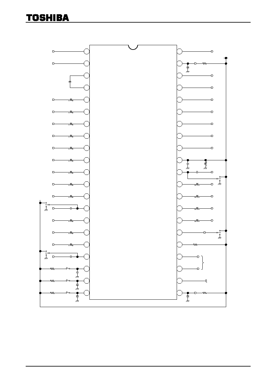
TA1218N/F
2000-09-11 38/40
Application Circuit
Note8: ( ): The terminal of TA1218F.
4
1
2
3
5
9
6
7
8
10
14
11
12
13
15
20
17
18
19
21
16
39
42
41
40
38
34
37
36
35
33
29
32
31
30
28
23
26
25
24
22
27
V
CC
=
9 V
0.
01
µ
F
2.2
µF
4.7 k
(43)
(44)
(45)
(46)
(47)
(48)
(2)
(3)
(5)
(6)
(7)
(8)
(9)
(10)
(11)
(12)
(13)
(15)
(16)
(17)
(18)
(42)
(41)
(40)
(39)
(38)
(37)
(36)
(35)
(34)
(33)
(30)
(29)
(28)
(27)
(26)
(25)
(24)
(23)
(22)
(21)
(19)
2.2
µF
47
µF
2.2
µF
2.2
µF
47
µF
2.2
µF
47
µF
2.2
µF
2.2
µF
47
µF
0.01
µF
2.2
µF
2.2
µF
47
µF
47
µF
2.2
µF
To
micro-
computer
0.01
µF
4.7 k
4.7 k
TA1218N/F
L
ou
t
2
R
out
2
Det in
Det Select
L
in
TV
R
in
TV
V
in
TV
L
in
V1
R
in
V1
V
in
V1
L
in
S1
Y/V
in
S1
R
in
S1
C
in
S1
L
in
S2
Y/V
in
S2
R
in
S2
C
in
S2
I/O1
I/O2
I/O3
V
out
2
O5
L
out
TV
R
out
TV
V
out
1
L
out
1
Y
out
R
out
1
C
out
V
CC
C
in
R
in
V2
Y
in
L
in
V2
V
in
V2
Address
Sync out
SDA
SCL
GND
O4
0.
01
µ
F
4.7 k
0.
01
µ
F
0.
01
µ
F
0.
01
µ
F
0.
01
µ
F
4.7 k
10 k
0.01
µF
0.
01
µ
F
100
µ
F

TA1218N/F
2000-09-11 39/40
Package Dimensions
Weight: 4.13 g (typ.)

TA1218N/F
2000-09-11 40/40
Package Dimensions
Weight: 0.83 g (typ.)