 | –≠–ª–µ–∫—Ç—Ä–æ–Ω–Ω—ã–π –∫–æ–º–ø–æ–Ω–µ–Ω—Ç: TA1276AFG | –°–∫–∞—á–∞—Ç—å:  PDF PDF  ZIP ZIP |
TA1276AFG
2002-04-01
1
TOSHIBA Bipolar Linear Integrated Circuit Silicon Monolithic
TA1276AFG
PAL
/
NTSC Video Chroma And Deflection IC For CTV
(normal scan/double scan mode)
TA1276AFG provides Video, Chroma and Deflection (sync, when double scan mode) circuit for a PAL/NTSC Color
TV, and suitable for a high picture quality, large screen size, wide
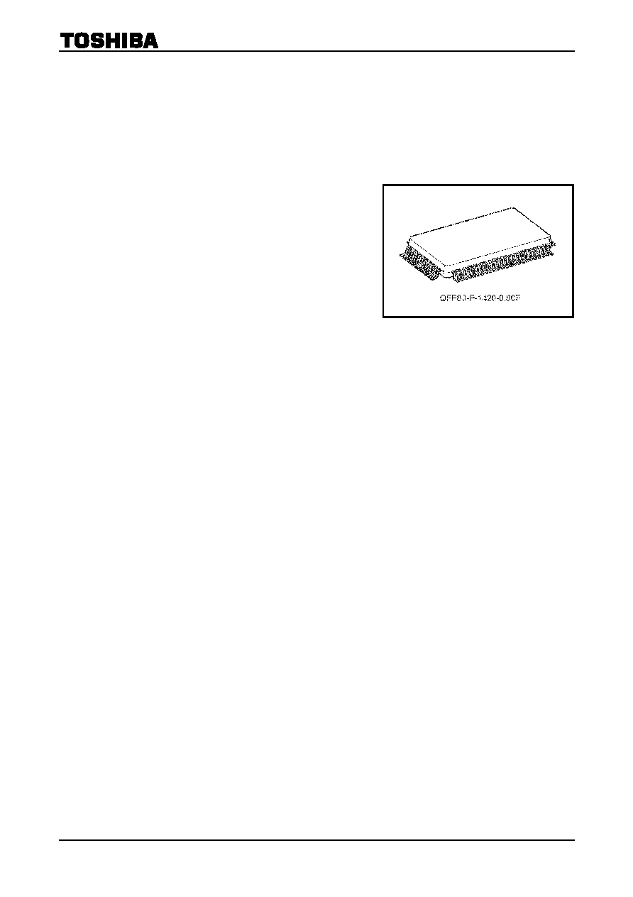
and/or double scanning TV. These functions are integrated in a 80
pin QPF plastic package.
TA1276AFG provides a high-performance video processor in
which a YUV double scanning signal can be applied in Video,
PAL/NTSC auto-detection circuit in Chroma and 50/60 Hz
auto-detection circuit in Sync. PAL demodulation circuit includes
Baseband signal processing system. And this demodulation
circuit does not required any adjustment.
TA1276AFG includes I
2
C bus interface, so you can adjust
various functions and controls via the bus.
Features
∑ Video/chroma section
∑ Y delay line
∑ Chroma trap
∑ IQ demodulation for NTSC, UV demodulation for PAL
∑ BEP (back end processor) section
∑ Enable to process a YUV signal independently
∑ Double scanning signal processing capability
(Y processing section)
∑ Black stretcher (controlled by I
2
C bus)
∑ DC restoration circuit (controlled by I
2
C bus)
∑ Highbright-color circuit
∑ D.L. aperture sharpness circuit + super real transcend circuit (LTI)
∑ correction (enable to control binary line, gain/start point)
∑ Y noise reduction circuit
∑ Velocity scan modulation output (the first order differential output and phase/amplitude adjustment)
(color difference section)
∑ Color detail enhancer
∑ Selectable relative phase and amplitude
∑ Flesh-color restoration
∑ Color circuit
∑ Baseband tint color
(text section)
∑ RGB primary color output
∑ On screen display interface
∑ Linear RGB interface
∑ Fast blanking
∑ Drive control
∑ AKB (only black level) or cut-off bus control
∑ Deflection section
∑ High performance sync. separation circuit
∑ Adjustment free H and V oscillation circuit by countdown system
∑ Horizontal and vertical position adjustment
∑ Sync separation, HD output
∑ Horizontal and vertical pulse output in normal mode.
Weight: 1.6 g (typ.)
TA1276AFG
2002-04-01
2
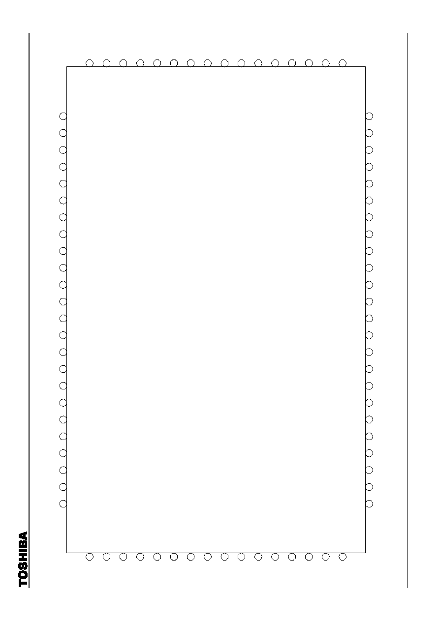
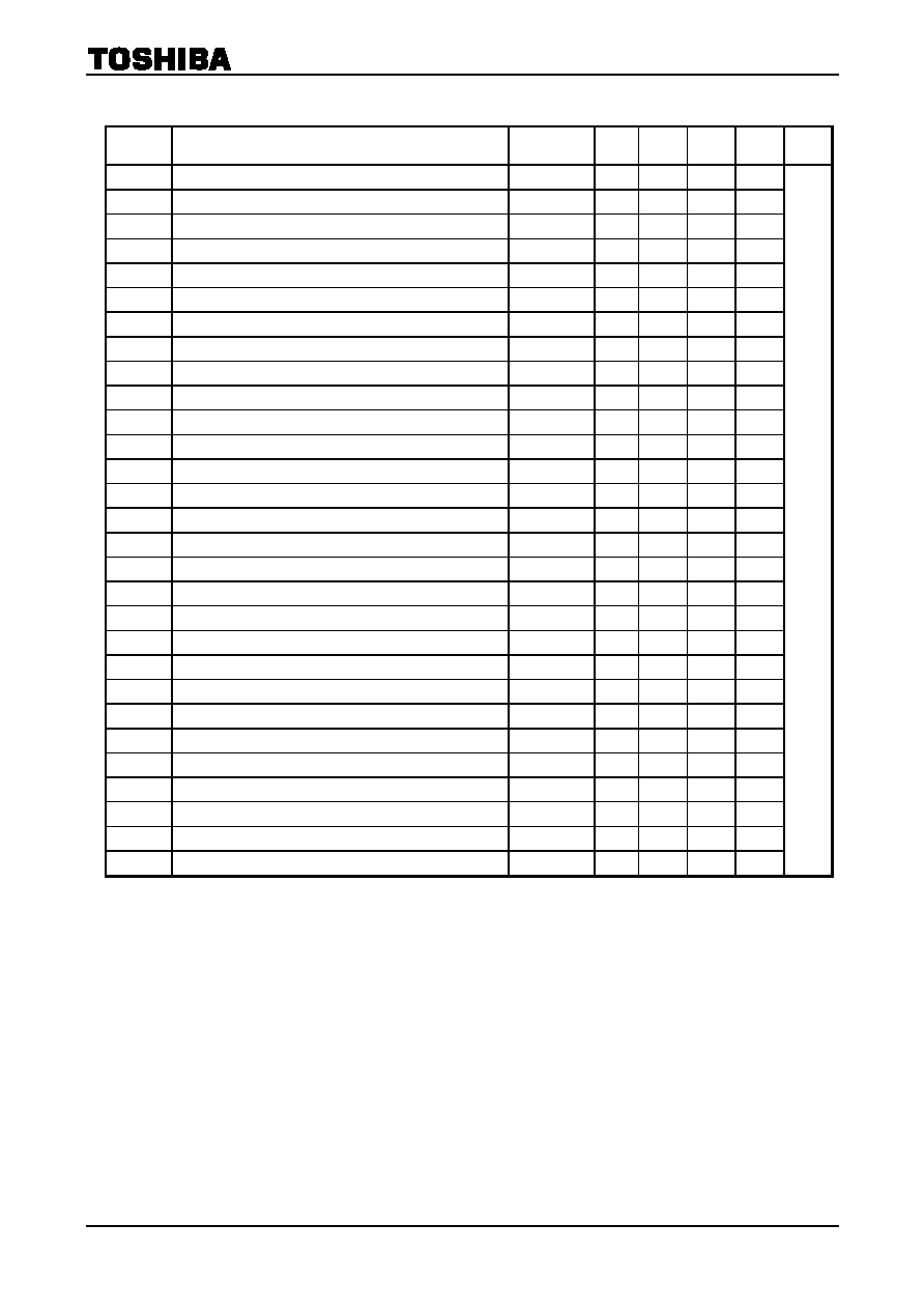
Pin Assignment
TA1276AFG
49
64
63
61
60
58
56
54
53
51
50
48
46
45
44
43
42
DE
F
V
CC
(9
V
)
32f
H
VC
O
NC
AFC
F
ilte
r
DE
F
GND
NC
HD Ou
t
V
.
S
ep.
NC
Chrom
a GND
Chrom
a
I
n
NC
APC
Fil
te
r
NC
M P
A
L
X
'
t
a
l
1H DL Con
t
V/I
O
u
t
41
Hori
zont
al
Out
p
ut
(
SW
)
62
4.
43 M
H
z X
'
t
a
l
59
3.
58 M
H
z X
'
t
a
l
57
V
CC1
(5 V
)
55
NC
52
Y
1
Sy
n
c
In
47
Sy
n
c
O
u
t
65
66
67
68
69
70
71
73
74
75
77
78
79
80 U/Q In
NC
Y2 In
NC
NC
R S/H
Sence In
NC
SCP Out
SECAM Conto
NC
Y
1
Out
NC
U/Q Out
72 f
sc
Out
76 Color Limiter
40
39
38
36
35
34
31
30
28
27
26
25
Analog B In
NC
Ys2 (analog RGB)
NC
NC
G S/H
SCL
SDA
NC
FBP In (BLK in)
NC
Curve odj.
(ext CP in)
29
VP Out
32
B S/H
33
NC
37
Digital GND
16
1
2
3
4
6
8
10
12
14
15
17
18
19
20
22
24
A
nal
og G
I
n
A
nal
og R
I
n
A
nal
og O
S
D B
I
n
A
nal
og O
S
D G
I
n
A
nal
og O
S
D R
I
n
V
CC2
(9 V
)
NC
B O
u
t
NC
NC
T
E
X
T
GND 1
ABC
L
In
YM
In
NC
APL
D
e
t.
Bla
c
k
Pe
a
k
H
o
ld
V/I
In
5
VSM
O
u
t
7
V
CC3
(9 V
)
9
T
E
X
T
GND 2
11
R Out
13
G Out
21
Y
s
1
(anal
og OS
D)
23
NC
TA1276AFG
2002-04-01
3
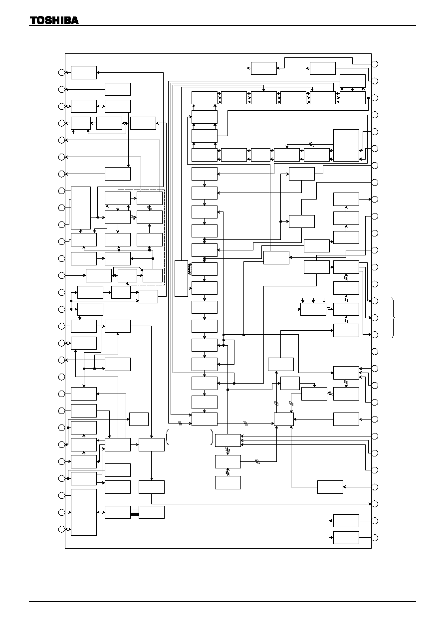
Block Diagram
∑ Pin 41 connect to V
CC
: Double Scan mode
Note 1: [ ]: for Double Scan mode only (external clamping pulse input mode)
Registor
D/A
Convert
H parabola
Phase Det
<AFC-2>
HD out/
BPP in
(Ext. VBLK)
H BLK
Delay Line
Sub Color
H Phase
Shift
32f
H
VCO
V Sep
H.V.
Sync Sep.
V Count
Down
Mode
SW
f
sc
Trap
SW
ACC Amp
TOF
SW
ACC Det
P/N
Ident Det
Filter Auto
Adj.
Chroma
Demond.
Delay Line
Color Sys
Ident
H Count
Down
Delay Line
TOF
LPF f
sc
Trap
CW
Matrix
Sharpness
Control
Correction
DC Restore
Black Level
Cor
Y Clamp
Black
Stretch
Tint
Uni-color
Half Tone
Uni-color
Clamp
Sub Cont
Y NR Amp
Chroma BLK
4.43 MHz
X'tal
Chroma GND
f
sc
Out
SCP Out
SECAM
Control
Y
1
Out
U/Q Out
V/I Out
1H DL
Control
M PAL X'tal
3.58 MHz
X'tal
APC Filter
V
CC1
(5 V)
Chroma In
Y
1
/Sync In
V-Sep.
HD Out
Sync. Out
DEF GND
AFC Filter
32f
H
VCO
DEF
V
CC
(9 V)
H. Out
[SW]
Curve Adjust
[Ext CP/
BPP In]
FBP In
[H/V BLK In]
Digital GND
SDA
SCL
Sharpness
Delay Line
SRT
R Out
G Out
B Out
100 IRE
=
2.3 V
p-p
I
2
C Bus
Decoder
H Drive
Phase Det
<AFC-1>
SECAM
Control
SW
f
sc
out
Chroma
VCO
APC Det
1 H DL
Control
SCP out
Sync out
Color
Axis G-Y
Matrix
Clamp
Half Tone
Color
Delay Line
SW
IQ
UV
Convert
Flesh Color
IQ/UV
Clamp
Black Peak
Det
APL Det
VSM
Mute
VSM Amp
HPF
DL SW
BLK
Clamp
Drive
RGB out
Y
M
SW
IK
R. G. B. S/H
OSD Amp
Ys SW
RGB
SW
SW
Clamp
ACL
ABCL Amp
RGB
Matrix
WPS
Internal Clamp Mode
or
External Clamp Mode
Contrast
Clamp
RGB
Bright
V Sync Sep
VP out
Ys SW
Cutoff
Cutoff
G S/H
B S/H
Hi Bright
Color
CDE
IK
Cutoff
Cutoff
R S/H
Sense In
R S/H
Color Limiter
Y
2
In
U/Q In
V/I In
Black Peak Hold
APL Det.
VSM Out
Y
M
In
ABCL In
Text GND 2
Text GND 1
V
CC2
(9 V)
Analog OSD
R In
Analog R In
Analog G In
Analog B In
VP Out
G S/H
B S/H
V
CC3
(9 V)
Analog OSD
G In
Analog OSD
B In
Ys1
(analog OSD)
Ys2
(analog OSD)
Color Peak
Det
Cutoff
72
38
40
41
34
35
37
46
47
49
42
43
45
54
57
58
50
52
53
63
64
65
59
61
62
67
69
70
73
25
24
22
31
29
27
18
17
15
21
20
19
9
8
7
13
11
10
2
1
80
6
5
3
78
76
74
32

TA1276AFG
2002-04-01
4
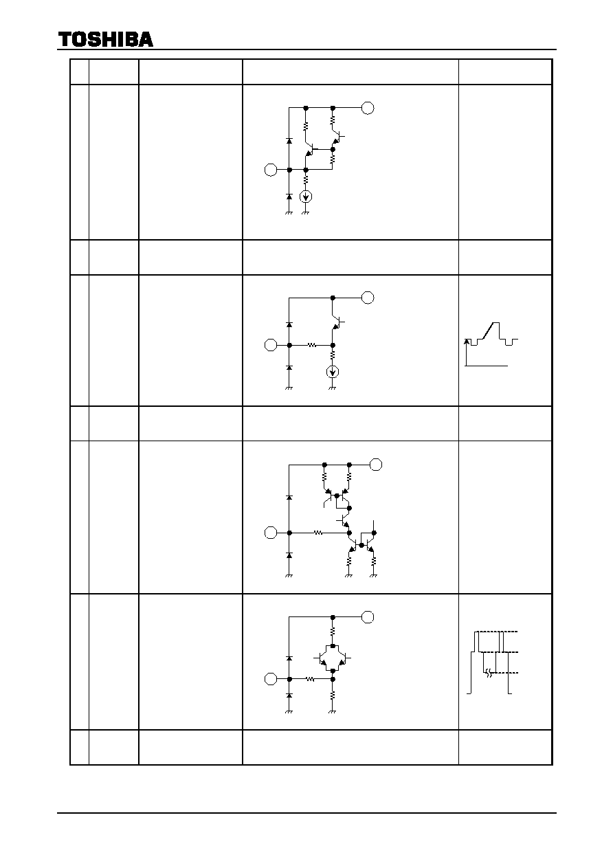
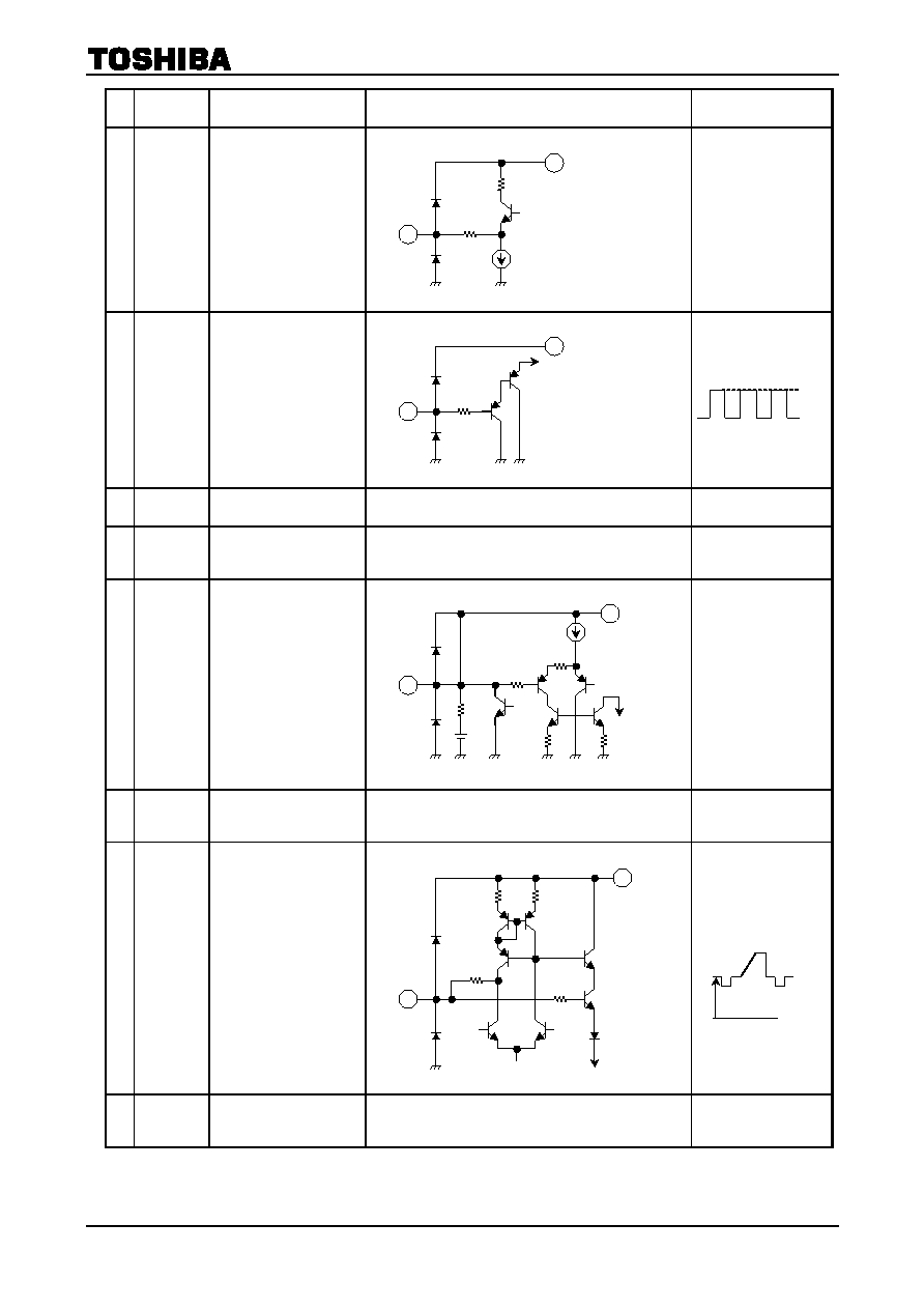
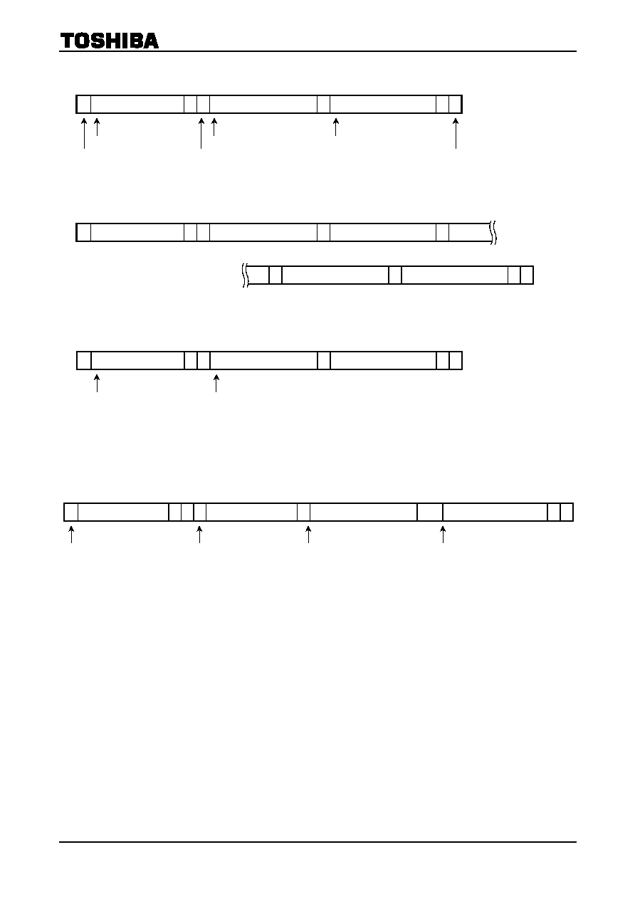
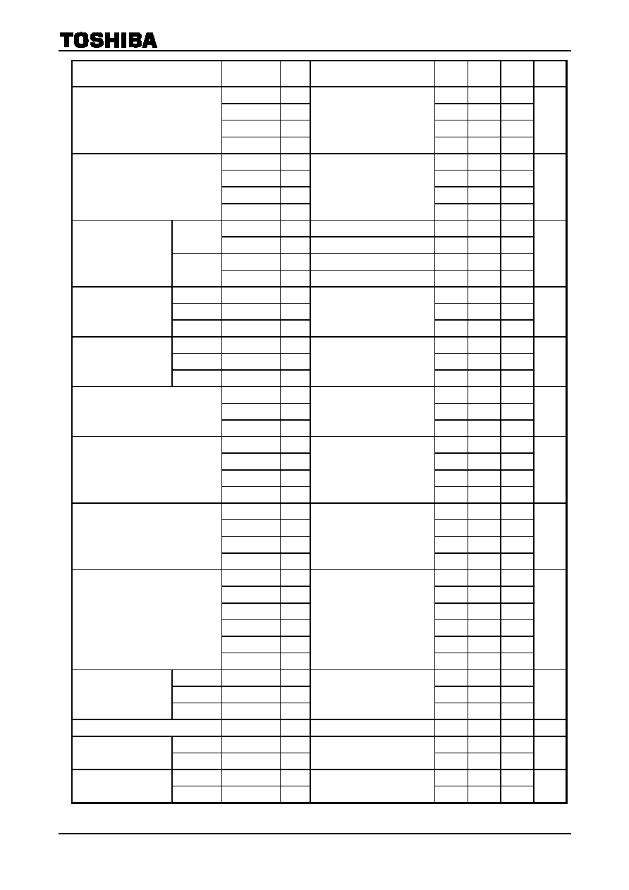
Terminal Functions
Pin
No.
Pin Name
Function
Interface Circuit
Input/Output
Signal
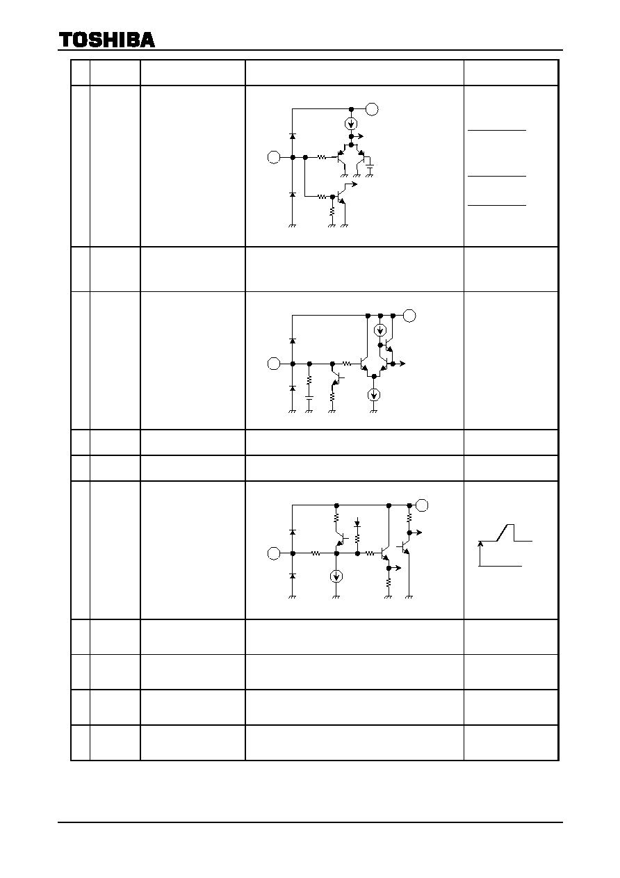
1
80
V/I input
U/Q input
The pin through which R-Y
(V)/I and B-Y (U)/Q
signals are input. Input via
clamp capacitor.
When Burst: Chroma
=
1:1
360
mV
p-p
DC:
5.0
V
2
Black peak
hold
Connect the filter
controlling the black
stretching gain of the
black stretching circuit.
The black stretching gain
varies depending on the
voltage at this pin.
DC
3 APL
detection
Connect the filter
correcting DC restoration
ratio.
Opening this pin can
monitor the Y-signal that
was subjected to black
stretching.
DC
4 NC
None connect PIN.
These pins connect to
GND.
5 VSM
output
Outputs the Y-signal that
routed HPF after it had
been subjected to DC
restoration.
The output is muted with
the switches of pins 32
and 36.
DC
3.5 V
7
1
80
7
2
200
1 k
4 k
1 k
1 k
5 V
4.
25 V
1 k
7
3
1 k
20 k
5 k
20 k
7
5
200
200
1 k
35 k
200
TA1276AFG
2002-04-01
5
Pin
No.
Pin Name
Function
Interface Circuit
Input/Output
Signal
6 YM
input
The half-tone switch for
internal RGB signal.
When the voltage at this
pin is set to 7.0 V or more,
the RGB output voltage.
7 V
CC3
(9 V)
The V
CC
pin of picture
quality and color
difference blocks.
Connect 9 V (typ.).
8 ABCL
input
Used to control the
external uni-color,
brightness, and dynamic
ABL.
Use this pin when using
ABL or ACL.
The sensitivity and starting
point of the ABL and
dynamic ABL can be set
by using bus.
ABCL OFF:
6 V or more
9 TEXT GND
2
The GND pin of TEXT
block.
10 TEXT GND
1
The GND pin of TEXT
block.
11
13
15
R output
G output
B output
Outputs RGB.
12 NC
None connect PIN.
These pins connect to
GND.
14 NC
None connect PIN.
These pins connect to
GND.
16 NC
None connect PIN.
These pins connect to
GND.
17 V
CC2
(9 V)
The V
CC
pin of the text
block.
Connect 9 V (typ.).
17
6
300
5 k
15 k
7.0 V
Soft AKB
0.75 V
Half Tone
GND
TV
17
8
5 k
30 k
30 k
17
200
100
11
13
15
1 k
10 k
100 k
100 k
100 IRE: 2.3 V
p-p
2.5 V
GND
At Cont max
BRT Cent.

TA1276AFG
2002-04-01
6
Pin
No.
Pin Name
Function
Interface Circuit
Input/Output
Signal
18
19
20
Analog
OSD R
input
Analog
OSD G
input
Analog
OSD
B input
The pin through which the
OSD signal or analog
RGB is input.
(1) When inputting an
OSD signal, input the
ODS signal with a
voltage of 0 to 5 V
(4.1 V or more).
(2) When inputting an
analog RGB, input the
RGB signal via clamp
capacitor.
ACL works on this
input signal only when
the entire screen is
YS1-HI (the entire
screen: OSD).
21 YS1
Switches between the
internal RGB signal and
OSD/analog RGB (pin 18,
19, 20). When this switch
is on, the VSM output is
muted.
22
24
25
Analog R
input
Analog G
input
Analog B
input
The pin through which the
analog RGB is input. Input
the RGB signal via clamp
capacitor.
23 NC
None connect PIN.
These pins connect to
GND.
26 NC
None connect PIN.
These pins connect to
GND.
27 YS2
Switches between the
internal RGB signal and
analog RGB (pin 33, 34,
35) signal.
When this switch is on, the
VSM output is muted.
28 NC
None connect PIN.
These pins connect to
GND.
17
1 k
1 k
18
19
20
100 IRE: 0.5 V
p-p
DC: 3.6 V
5 V
0 V
(1)
(2)
17
21
1.3 k
50 k
2.25 V
OSD
0.75 V
VSM Mute
GND
TV
100 IRE: 0.5 V
p-p
3.5 V GND
17
1 k
1 k
22
24
25
17
27
1.3 k
50 k
0.75 V
GND
TV
A. BGB

TA1276AFG
2002-04-01
7
Pin
No.
Pin Name
Function
Interface Circuit
Input/Output
Signal
29 VP
output
Outputs the vertical pulse.
This pin also serves as the
external blanking input.
When current stronger
than
350
µ
A flows, blanking
takes place due to the
internal blanking and OR
logic circuit.
30 NC
None connect PIN.
These pins connect to
GND.
31
32
G S/H
B S/H
These pins are to be
connected with a capacitor
for sampling and holding a
bais voltage in the AKB
operation, of for clamping
to set DC voltage of RGB
outputs in the no-AKB
mode.
DC
33 NC
None connect PIN.
These pins connect to
GND.
34 SCL
The SCL pin of I
2
C bus.
35 SDA
The SDA pin of I
2
C bus.
36 NC
None connect PIN.
These pins connect to
GND.
42
29
200
5 k
1.
5 k
4.
25 V
5 k
200
µ
A
0 V
5 V
17
500
31
32
74
1 k
AKB
or
Clamp
200
5 k
5 k
5 k
1 k
R/G/B
200
200
50 k
Soft
AKB
(bus)
42
34
20 k
SDA
3 V
100
µ
F
42
35
50
20 k
SDA
ACK
3 V
TA1276AFG
2002-04-01
8
Pin
No.
Pin Name
Function
Interface Circuit
Input/Output
Signal
37 Digital GND The GND pin of I
2
L block.
38 FBP
input
The pin through which
FBP is input to generate
pulses for horizontal
AFC2, Y smoothing, and
horizontal blanking.
When double SCAM
mode, input H blanking
pulse (5 V or over).
39 NC
None connect PIN.
These pins connect to
GND.
40
Curve
correction
(ext.
CP/BPP
input)
(1) Used to correct
distortion of picture in
the case of
high-tension
fluctuation. Input the
AC component of
high-tension
fluctuation.
To disactivate the
distortion correction
feature, connect a
capacitor of 0.01
µ
F
between this pin and
GND.
(2) Double scan mode
This pin is to input
external CP (clamping
pulse) and BPP
(black peak detection
stopping pulse).
41
Horizontal
output
(mode SW)
Produces the horizontal
output.
Connecting the DEF V
CC
to this pin can swich
Double Scan mode. In this
case, the horizontal output
is not produced.
HIGH: 3.2 V
LOW: 0.2 V
42
DEF V
CC
(9 V)
The V
CC
of DEF block.
Connect 9 V (typ.) to this
pin.
42
38
200
8.
25 V
2.
25 V
1.
0 V
FBP
3.
5 V
3.
5 V
1.0 V
(H BLK)
3.5 V
(AFC-2)
9 V
42
40
45 k
2.
5 V
45 k
45 k
45 k
AFC-2
0 V
5 V
1.5
µ
s
Ext BPP
Ext BPP TH: 1.0 V
Ext. Clamp Pulse
Ext. CP
TH: 3.6 V
(1) DC
4.5
V
(2)
42
41
5 k
50 k
15 k
30 k
30 k
1.
5 V
7.
5 V
TA1276AFG
2002-04-01
9
Pin
No.
Pin Name
Function
Interface Circuit
Input/Output
Signal
43 32f
H
VCO
Connect the ceramic
oscillator for horizontal
oscillation.
The oscillator to be used
is CSBLA503KECZF30,
made by Murata
electronics.
44 NC
None connect PIN.
These pins connect to
GND.
45 AFC
filter
Connect the filter for
horizontal AFC.
The frequency of the
horizontal output varies
depending on the voltage
at this pin.
DC
46 DEF
GND The GND pin of DEF
block.
47 SYNC.
output
Output the synchronizing
signal that was separated
in the synchronous
separation circuit.
This pin is of the open
collector system. Connect
the pull-up resistor.
48 NC
None connect PIN.
These pins connect to
GND.
49 HD
output
(1) When BUS HD-OUT
=
0
Output the HD pulse
(pulse duration: 1
µ
s)
together with AFC.
This pin also serves
as the external input
pin that accepts BPP
(black peak detection
stopping pulse)
signal.
(2) When BUS HD-OUT
=
1
When AKB mode is
ON, the pulse which
covers AKB reference
period is output.
42
43
1 k
47 k
10 k
10 k
3 k
1 k
130 mV
p-p
DC: 5.9 V
42
45
300
30 k
7.
5 V
42
47
200
5 V
GND
42
49
200
1 k
HD
5 k
6.
5 V
Ext. BPP
0 V
5 V
1
µ
s
Ext BPP
BPP TH: 1.0 V
HD
0 V
5 V
(2)
(1)
TA1276AFG
2002-04-01
10
Pin
No.
Pin Name
Function
Interface Circuit
Input/Output
Signal
50 V-Sep.
Connect the filter
separating the vertical
synchronization.
DC6.4 V
51 NC
None connect PIN.
These pins connect to
GND.
52 Y
1
/SYNC
input
The pin through which the
composite video signal or
Y signal is input. Input via
clamp capacitor.
53 Chroma
GND
The GND pin of the
chroma processing block.
54
Chroma
input
The pin through which the
chroma is input. Input the
chroma signal that was
subjected to Y/C
separation.
55 NC
None connect PIN.
These pins connect to
GND.
56 NC
None connect PIN.
These pins connect to
GND.
57 V
CC1
(5 V)
The V
CC
of the chroma
and I
2
C Bus blocks.
Connect 5 V (typ.)
42
50
500
57
52
1 k
1 k
30 k
18 k
6 k
1 V
p-p
2.5 V
GND
57
54
1 k
10 k
10 k
2.
5 V
Burst level:
300 mV
p-p
2.5 V
GND
TA1276AFG
2002-04-01
11
Pin
No.
Pin Name
Function
Interface Circuit
Input/Output
Signal
58 APC
filter
Connect APC filter
demodulating the chroma.
The oscillation frequency
of VCXO varies depending
on the voltage at this pin.
DC
60 NC
None connect PIN.
These pins connect to
GND.
62
61
59
4.43 MHz
X'tal
M PAL X'tal
3.58 MHz
X'tal
Connect X'tal. In the case
of series capacity, the
oscillation frequency (f
0
)
can be changed. In the
case of parallel capacity,
the changeable range of
frequency can be
changed.
DC
4.0 V
90 mV
p-p
63 1H DL
control
Outputs the result of
whether the signal is PAL,
SECAM or NTSC.
Connect the output to the
1H DL IC.
In the case of
discrimination between
white or black, the voltage
just before that is retained.
The voltage immediately
after turning-on is not
fixed.
8.4 V: PAL
4.3 V: SECAM
0 V: NTSC
64 V/I
output
Outputs R-Y (V) or Q
signal. It includes LPF that
can remove carrier.
The chroma signal that
routed ACC and TOF
circuits (before demo
input) can be monitored by
pulling up this pin at 10
k
.
DC
2.5 V
Rainbow
color bar
: 360 mV
p-p
57
58
2 k
3 k
1 k
600
57
3 k
R
500
62
61
59
R
Pin 62 1.5 k
Pin 61 2.5 k
Pin 59 2.5 k
42
63
500
5 k
89 k
57
64
400
µ
F
1 k
30 k
1 k
TA1276AFG
2002-04-01
12
Pin
No.
Pin Name
Function
Interface Circuit
Input/Output
Signal
65 U/Q
output
Outputs B-Y (U) or I
signal.
It includes LPF that can
remove carrier.
DC
2.5 V
Rainbow
color bar
: 360 mV
p-p
66 NC
None connect PIN.
These pins connect to
GND.
67 Y
1
output
Outputs the Y signal that
routed the f
sc
TRAP
(TRAP can be turned on
or off with bus.) and the Y
delay line circuit.
68 NC
None connect PIN.
These pins connect to
GND.
69
SECAM
control
The input/output pin that is
used to control the
SECAM demodulation IC.
When current stronger
than 250
µ
A flows from
this pin, that is recognized
as SECAM.
When
PAL/NTSC
4.0 V
When SECAM
0.75 V
70 SCP
output
Outputs SCP (sand castle
pulse).
The output signal consists
of clamp pulse, horizontal
blanking pulse, and
vertical blanking.
The minimum load
resistance is 3 k
.
71 NC
None connect PIN.
These pins connect to
GND.
57
65
400
µ
F
1 k
30 k
1 k
57
67
300
1 m
A
1 V
p-p
2 V
GND
42
69
500
2 k
10 k
42
70
200
8 k
200
8.3 V
4.8 V
2.5 V
GND
TA1276AFG
2002-04-01
13
Pin
No.
Pin Name
Function
Interface Circuit
Input/Output
Signal
72 f
sc
output
Outputs oscillation
waveform of VCXO.
When 3.58 NTSC killer-off
this pin voltage sets 3.2 V.
When B/W or other
systems killer-off, this pin
voltage sets 1.4 V.
DC
3.58
NTSC
: 3.2 V
B/W or Others system
: 1.4 V
AC
0.6 V
p-p
73 SENSE
input
This pin is to sense IK
voltage feed-back from a
CRT Drive circuit.
74 R
S/H
The same as pin 31 and
32.
The same as pin 31 and 32.
DC
75 NC
None connect PIN.
These pins connect to
GND.
76
Color
limiter
Color the filter detecting
the color limit.
DC
77 NC
None connect PIN.
These pins connect to
GND.
78 Y
2
input
The pin through which B-Y
(V)/I and R-Y (U)/Q
signals are input. Input via
clamp capacitor.
79 NC
None connect PIN.
These pins connect to
GND.
57
72
200
200
1 m
A
17
73
500
SENSE
1.5 V
R G B
7
76
5 k
30 k
5 V
10 k
2 k
7
78
1 k
1 k
5 k
5 k
1 V
p-p
(both signals)
6.3 V
GND

TA1276AFG
2002-04-01
14
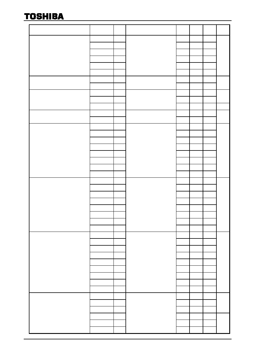
Bus Control Map
Write Mode
Slave Address: 88H (10001000)
Preset
Sub
Address
D
7
MSB
D
6
D
5
D
4
D
3
D
2
D
1
D
0
LSB
MSB LSB
00 P-MUTE
UNI-COLOR
1000 0000
01 BRIGHTNESS
1000
0000
02 COLOR
Y-MUTE
1000
0000
03 TINT
YM-SW
1000
0000
04 SHARPNESS
YNR
1000
0000
05 RGB
BRIGHTNESS
WPS
L
1000
0000
06 HI
BRT
RGB
CONTRAST
1000 0000
07 SUB
COLOR COLOR
CLT
1000
0000
08 SUB
CONTRAST Y-
CURVE
FLESH
1000
0000
09 G
(R)
DRIVE
DR-SW
1000
0000
0A B
DRIVE
CDE
1000
0000
0B HORIZONTAL
POSITION
HV-SepL
V-OFF
H-BLK
1000
0000
0C R
CUT
OFF
1000
0000
0D
G CUT OFF
1000
0000
0E B
CUT
OFF
1000
0000
0F
R-Y PHASE
R/B GAIN
G/B GAIN
G-Y PHASE
0000
0000
10
COLOR SYSTEM
P/N-ID
BB SW
OSD-SL
OS-ACL
TX-ACL
0000
0000
11
VSM PHASE
VSM GAIN
APACON PEAK f
0
VSM-PB
0000
0000
12
DC RESTORATION POINT
DC RESTORATION RATE
DC REST. LIMIT
0000
0000
13
BLACK STRETCH POINT
APL VS BSP
Y-
PNT
VSM-H.PB FREQ
0000
0000
14 SHR-TRACKING
TEST
RGB-
B.L.C. B.S.G. B.D.L. BS-ARE 0000 0000
15
DYNAMIC ABL POINT
DYNAMIC ABL GAIN
AKB MODE
0000
0000
16
ABL POINT
ABL GAIN
RGB OUT MODE
0000
0000
17
HD-OUT
V-BLK
VERTICAL FREQUENCY
VERTICAL POSITION
0000
0000
18 Y-DL
C-TRAP
TOF
f
0
TOF-Q
0000
0000
Read Mode
Slave Address: 89H (10001001)
D
7
D
6
D
5
D
4
D
3
D
2
D
1
D
0
0
PORSET COLOR
SYSTEM
X'tal
V-FREQ V-STD H-LOCK
1 N-DET
RGBOUT
Y
1
-IN IQ-IN Y
2
-IN H-OUT
VP-OUT IK-IN

TA1276AFG
2002-04-01
15
Bus Control Feature
Write Mode
Item Explain
Preset
P-MUTE
Picture mute SW; (0): OFF, (1): ON
ON
UNI-COLOR Uni-color
adjustment;
-
18dB to 0dB
Center
BRIGHTNESS
Brightness adjustment (including sub adjustment);
-
40 IRE to
+
40 IRE
Center
COLOR Color
adjustment;
-
20dB (color mute) to
+
4dB 0dB
Y-MUTE
Y mute SW; (0): ON, (1): OFF
ON
TINT Hue
adjustment;
-
32∞ to
+
32∞ 0∞
TM-SW
Half-tone SW (YUV input); (0): OFF, (1): ON
OFF
SHARPNESS Sharpness
adjustment;
-
20dB to
+
14dB
+
8dB
YNR
Y Noise Reduction SW; (0): OFF, (1): ON
OFF
RGB BRIGHTNESS
RGB Brightness Adjustment;
-
20 IRE to
+
20 IRE
0 IRE
WPS L
White Peak Suppression Level; (0): 130 IRE, (1): 110 IRE
130 IRE
HI BRT
High-bright color; (0): OFF, (1): ON
OFF
RGB CONTRAST
RGB Contrast;
-
18dB to 0dB
-
18dB
SUB COLOR
Sub-color;
-
4dB to 0dB to
+
3dB 0dB
COLOR
Color
correction point;
(00): OFF, (01): 0.2 V
p-p
, (10): 0.4 V
p-p
, (11): 0.6 V
p-p
OFF
CLT
Color Limiter Level; (0): 1.8 V
p-p
, (11): 2.2 V
p-p
1.8
V
p-p
SUB CONTRAST
Sub-contrast adjustment;
-
3dB to
+
3dB 0dB
Y-
CURVE
Y-
curve switching;
(00): OFF, (01):
-
2.5dB, (10):
-
5.6dB, (11):
-
7dB
OFF
FLESH
Flesh color; (0): OFF, (1): ON
OFF
G (R)/B DRIVE
R (G)/B drive gain adjustment;
-
5dB to 0dB to
+
3dB 0dB
(40h)
DG-SW
Drive gain base axis switching; (0): G, (1): R
G
CDE
Color Detail Enhancer;
(0): ON (foced OFF when sharpness go through), (1): OFF
ON
HORIZONTAL POSITION
Horizontal position adjustment;
-
3
µ
s to
+
3
µ
s 0
µ
s
HV-SepL
Sync separation level; (from SYNC TIP) (0): 35%, (1): 40%
35%
V-OFF
Vertical output SW; (0): ON, (1): OFF
ON
H-BLK
Horizontal blanking SW; (0): ON, (1): OFF
ON
R/G/B CUTOFF
R/G/B cut-off adjustment;
∑
When AKB-OFF: RGB output 2 V to 2.5 V to 3 V
∑
When AKB-ON: SENS input
1
V
p-p
to 1.5 V
p-p
to 2 V
p-p
(
±
5 IRE)
Center
(80h)
R-Y PHASE
R-Y relative phase switching;
(00): 90∞, (01): 92∞, (10): 94∞, (11): 112∞
90∞
R/B GAIN
R/B relative amplitude switching;
(00): 0.56, (01): 0.68, (10): 0.79, (11): 0.86
0.56
G/B GAIN
G/B relative amplitude switching;
(00): 0.3, (01): 0.34, (10): 0.4, (11): 0.45
0.3
G-Y PHASE
G-Y relative phase switching;
(00): 236∞, (01): 240∞, (10): 244∞, (11): 253∞
236∞

TA1276AFG
2002-04-01
16
Item Explain
Preset
COLOR SYSTEM
Color system;
System X'tal Color Color TINI
difference
difference
control
mute
input
(000): NTSC
3.58
Forced
OFF
I/Q
Enable
(001): NTSC
3.58
Forced
OFF
U/V
Enable
(010): NTSC
4.43
Forced
OFF
U/V
Enable
(011): PAL
4.43
(N) Forced
OFF
U/V
Enable
(100): PAL
M
Forced
OFF
U/V
Enable
(101): SECAM
4.43
Forced OFF
U/V
Enable
(110): MULTI
3.58/4.43 Forced OFF
U/V
Enable
(111): Trinorma
3.58/M/N Forced OFF
U/V
Enable
NTSC
(000)
P/N ID
PAL/NTSC ident sensitivity switching;
(0): LOW (when digital comb filter used), (1): Normal
LOW
BB SW
Blue Back SW; (0): OFF, (1): ON
OFF
OSD-SL
OSD peak suppressing level switching; (0): 96 IRE, (1): 76 IRE
96 IRE
OS-ACL
OSD ACL SW; (0): ON, (1): OFF
ON
TX-ACL
RGB ACL SW; (0): Gain 1/2, (1): Normal
Gain1/2
VSM PHASE
VSM output phase switching;
(00):
-
40 ns, (01):
-
20 ns, (10): 0 ns, (11)
+
20 ns
-
40 ns
VSM GAIN
VSM output gain switching;
(00): 0dB, (01):
-
6dB, (10):
-
9dB, (11): OFF
0dB
APACON PEAK f
0
Apacon peak frequency switching;
(000): Through (apacon off), (001): 4.0 MHz,
(010): 3.3 MHz, (011): 2.5 MHz,
(100): Through (apacon off), (101): 13 MHz,
(110): 10 MHz, (111): 8 MHz
(000)
Through
VSM PB
VSM output horizontal parabolic modulation SW;
(0): Parabolic modulation OFF,
(1): ON (nearby sharpness
-
3dB)
Parabolic
modulation
OFF
DC RESTORATION POINT
DC restoration start point; (000): 0% to (111): 42%
0%
DC RESTORATION RATE
DC restoration rate; (000): 100% to (111): 130%
100%
DC REST. LIMIT
DC restoration limit point; (APL)
(00): 100%, (01): 87%, (10): 73%, (11): 60%
100%
BLACK STRETCH POINT (BSP) Black stretcher start point; When APL 0%
(000): 22 IRE to (111): 56 IRE
22 IRE
APL VS BSP (AVS)
APL level vs. black stretcher start point;
(00): 0dB to (11): 1.5dB, BSP
+
APL
◊
BSP
◊
AVS
0dB
Y-
PNT
Y-
point switching; (0): 100 IRE, (1): 95 IRE
100 IRE
VSM-H. PB FREQ
VSM output horizontal parabolic frequency;
(00): 15.7 kHz, (01): 24.8 kHz, (10): 31.5 kHz, (11): 33.75 kHz
SHR-TRACKING
Sharpness tracking; (00): HIGH, (11): LOW
HIGH
TEST
Test mode; (0): NORMAL
(1): Test mode (for factory test)
Switched by sub-address 17H
<
during gate-pulse
>
D
2
(0): during V-BLK, (1): NORMAL
Y/RGB smoothing OFF, Monitor of DAC at HD output
NORMAL
RGB-
RGB-
SW; (0): OFF, (1): ON
OFF
B.L.C.
Block level automatic correction (priority over black stretcher);
max 7.5 IRE (0): OFF, (1): ON
OFF
B.S.G.
Black stretcher gain SW; (0) ON, (1): OFF
ON
B.D.L.
Black detection SW; (0): 3 IRE, (1): 0 IRE
3 IRE
BS-ARE
Black area reinforcement SW;
For wide TV (when using time axis compression IC)
(0): ON, (1): OFF
ON
DYNAMIC ABL POINT
Dynamic ABL detection voltage; (000): min to (111): max
min

TA1276AFG
2002-04-01
17
Item Explain
Preset
DYNAMIC ABL GAIN
Dynamic ABL sensitivity; (000): min to (111): max
min
AKB MODE
AKB MODE; Only black level
(00): AKB OFF
+
S/H LOW, (01): AKB OFF
+
Cutoff BUS
(10): AKB ON
+
I-DET NORMAL, (11): AKB ON
+
I-DET
◊
3
(00)
AKB OFF
+
S/H LOW
ABL POINT
ABL detect voltage; (000): min to (111): max
min
ABL GAIN
ABL GAIN; (000): min to (111): max
min
RGB OUT MODE
RGB output mode SW;
(00): NORMAL, (01): Only R, (10): Only G, (11): Only B
NORMAL
HD-OUT
HD output SW; (0): HD output, (1): AKB period pulse
HD output
V-BLK
Vertical Blanking SW; (0): ON, (1): OFF
ON
VERTICAL FREQUENCY
Vertical Frequency;
(000): AUTO (50, 60 Hz),
(001): AUTO (50, 60 Hz/V MASK OFF),
(010): 60 Hz,
(011): 60 Hz (V MASK OFF),
(100): Forced 262.5H,
(101): Forced 263H,
(110): Forced 312.5H,
(111): Forced 313H,
When (100), (101), (110), (111): AFC Free-run
(000)
AUTO
VERTICAL POSITION
Vertical position; (000): 0H to (111): 7H (1H STEP)
0H
Y-DL
Y-DL SW; (0) OFF, (1): ON (
+
80 ns)
OFF
C-TRAP
Chroma Trap SW; (0): OFF, (1): ON
OFF
TOF-f
0
Selectable TOF Peak Frequency;
(000): 0.8f
sc
+
TOF OFF to (111): 1.5f
sc
TOF OFF
TOF-Q
Selectable TOF Q; (000): 0.6 to (111): 1.2
0.6
TA1276AFG
2002-04-01
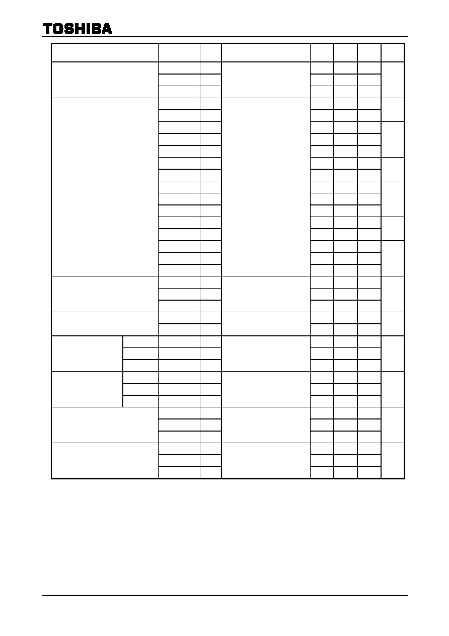
18
Delay Time From Y
1
Input (PIN 52) to Y
1
Output (PIN 67)
Color Trap
Y-DL
Delay
Time
B/W
OFF
ON
295 ns
375 ns
OFF
OFF
OFF
ON
ON
295 ns (4.43)
295 ns (3.58/M/N)
375 ns (4.43)
375 ns (3.58/M/N)
PAL/NTSC
ON
OFF
OFF
ON
ON
295 ns (4.43)
310 ns (3.58/M/N)
375 ns (4.43)
390 ns (3.58/M/N)
SECAM
OFF
ON
495 ns
575 ns
Read Mode
Characteristic Explain
PORSET
Power On Reset; (0): RESISTER PRESET, (1): NORMAL
COLOR SYSTEM
Color system; Receiving system (judgement of ID ON/OFF)
(00): B/W, (01): SECAM, (10): PAL, (11): NTSC
X'tal X'tal
Mode;
(00):
, (01): 4.43 (N), (10): M, (11): 3.58
V-FREQ
Vertical frequency; (0): 50 Hz, (1): 60 Hz
V-STD
Vertical Standard ident; (0) NON-STANDARD, (1): STANDARD
H-LOCK
Horizontal Lock ident; (0): LOCK, (1): UN-LOCK
N-DET
Noise ident result; (0): FEW, (1): MANY
RGBOUT, Y
1
-IN, IQ-IN, Y
2
-IN,
H-OUT, VP-OUT
Self-ident result; (0): NG, (1): OK
IK IN
IK input ident result; (0): NG, (1): OK
TA1276AFG
2002-04-01
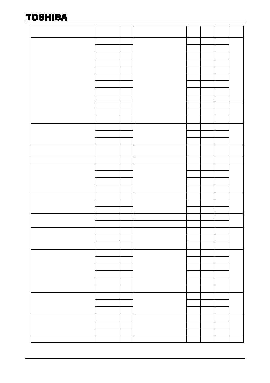
19
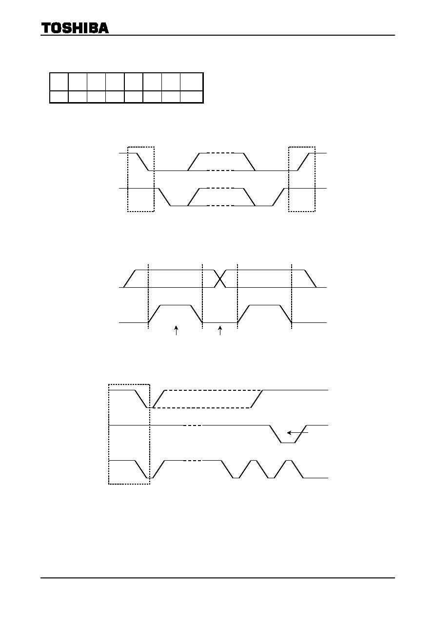
I
2
C Bus Transmission/Receiving
Slave Address: 88H
A
6
A
5
A
4
A
3
A
2
A
1
A
0
W/R
1 0 0 0 1 0 0 0/1
Start/Stop Condition
Bit Transmission
Confirmation Response
SDA
SCL
S
Start condition
P
Stop condition
SDA
SCL
SDA is not allowed to changed.
SDA is not allowed to changed.
SDA from
Transmitter
S 9
8
1
High impedance at 9
th
bit
Low impedance only at 9
th
bit
SDA from
Receiver
SCL from
Master
High impedance
TA1276AFG
2002-04-01
20
Data Transmit Format 1
Data Transmit Format 2
Data Receive Format
At the moment of the first acknowledge, the master transmitter becomes a master receiver and the slave
receiver becomes a slave transmitter. This acknowledge is still generated by the slave.
The STOP condition is generated by the master.
Optional Data Transmit Format: Automatic Increment Mode
In this transmission method, data is set on automatically incremented sub-address from the specified
sub-address.
Purchase of TOSHIBA I
2
C components conveys a license under the Phillips I
2
C Patent Rights to use
these components in an I
2
C system, provided that the system conforms to the I
2
C standard Specification as
defined by Phillips.
S
Slave address
0 A
Sub address
A
Transmit data 1
A
------
------ A
Sub address
A
Transmit data n
A P
7 bit
8 bit
MSB
MSB
S
Slave address
1 A
Receive data 01
A
Transmit data 02
A P
MSB
7 bit
7 bit
8 bit
MSB
MSB
MSB
S
Slave address
0 A 1
Sub address
A
Transmit data 1
------
Transmit data n
A P
8 bit
7 bit
8 bit
8 bit
S: Start condition
MSB
A: Acknowledge
MSB
P: Stop condition
MSB
S
Slave address
0 A
Sub address
A
Transmit data
A P
TA1276AFG
2002-04-01
21
Pin 41 H-out (mode SW)
You can select the Double Scan Mode (external CP (clamping pulse) input mode), by connecting Pin 41 to
DEF V
CC
. (the threshold of pin 23: 8.7 V = DEF V
CC
- 0.3 V)
When Double Scan Mode, function of Pin 38 and 40 are changed.
∑ Normal Scan (internal CP) Mode: Pin 41 H-out
The function of Pin 40 is curve correction input, that of Pin 38 is FBP (flay back pulse) input.
The input signals of Y
2
, U/I and V/I inputs (pin 1, 2 and 3), Analog OSD inputs (pin 18, 19 and 20),
Analog RGB inputs (pin 22, 24 and 25) are clamped of the internal CP based on the Y
1
/Sync input (pin
52).
∑ Double Scan (external CP input) Mode: Pin 41 H-out
The function of Pin 40 is EXT/BPP (Note 2) input, that of Pin 38 is H/V BLK (blanking) input.
The input signals of Y
2
, U/I and V/I inputs (pin 1, 78 and 80), Analog OSD inputs (pin 18, 19 and 20),
Analog RGB inputs (pin 22, 24 and 25) are clamped of the external CP based on Pin 40.
In case of Double Scan Mode, bus "V-BLK" should be set (1); OFF.
Terminal Functions
Mode
Pin No.
Normal Scan Mode
(internal CP)
Double Scan Mode
(external CP input)
Pin 41
H-out
DEF V
CC
(9 V)
Pin 40
Curve correction signal input
EXT CP/BPP input
Pin 38
FBP input (for AFC-2 detection, H BKL)
H/V BLK input (for RGB H/V BLK, AKB)
Pin 1, 78, 80
Pin 18, 19, 20
Pin 22, 24, 25
Clamping by internal CP
(based on pin 52)
Clamping by external CP
(based on pin 40)
Pin 52
Normal scan; Y/Sync signal input
Pin 49
Normal scan; HD pulse output (based on pin 52)
Pin 29
Normal scan; VP output (based on pin 52)
Note 2: BPP: Black Peak detection stopping Pulse
TA1276AFG
2002-04-01
22
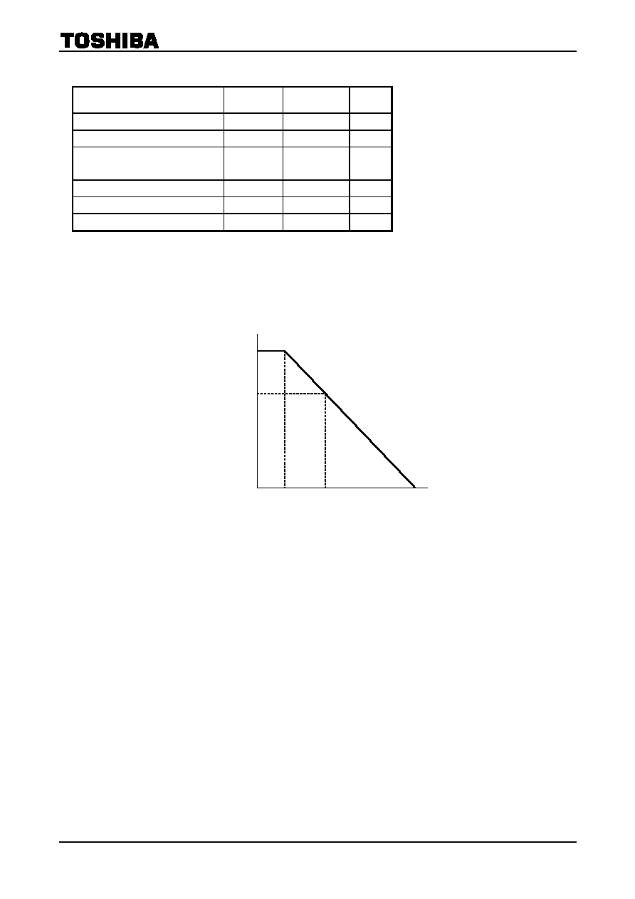
Maximum Ratings
(Ta
=
=
=
= 25∞C)
Characteristics Symbol
Rating
Unit
Supply voltage
V
CCmax
12 V
Input terminal voltage
e
inmax
9 V
p-p
Power dissipation
P
D
(Note 3)
2500 mW
Power dissipation reduction rate
1/
ja 20.0
mW/∞C
Operating temperature
T
opr
-
20 to 70
∞C
Storage temperature
T
stg
-
55 to 150
∞C
Note 3: Refer to the figure below. (with device mounted on a PCB whose dimensions are 114.3 mm
76.2 mm
◊
1.6 mm and whose surface is 20% copper.
mount the device on a PCB of at least these dimensions and whose surface is at
least 20% copper.)
Note 4: Short pins 9 and 10 together on the PCB.
Figure 1 Power Dissipation Reduction Against Higher Temperature
2500
150
25 70
1600
P
o
wer
dissi
pati
on P
D
(mW
)
Ambient temperature Ta (∞C)
TA1276AFG
2002-04-01
23
Recommended Condition In Use
Characteristic Description
Min
Typ.
Max
Unit
Pin
65
4.3 5.0 5.3
Supply Voltage
Pin 42, Pin 17, Pin 7
8.7
9.0
9.3
V
Y
1
/Sync, Y
2
Input Signal Level
White: 100%, including,
synchronization
(synchronization: minus)
0.9 1.0 1.1 V
p-p
When TOF OFF (burst level)
200
300
400
Chroma Input Signal Level
When TOF ON (burst level)
100
200
300
mV
p-p
I/Q, U/V Input Level
B:C
=
1:1
300
mV
p-p
When OSD input (DC coupling)
4.2
5.0 V
OSD/Analog RGB Input Level
When analog RGB input (AC coupling)
0.4
0.5
0.6
Analog RGB Input Level
0.4 0.5 0.6
V
p-p
FBP Width
11 12 13
µ
s
FBP Input Current
1.5
RGB Output Current
1.0 2.0
H. OUT Output Current
3.0 10.0
Pin 47 Input Current
0.5 1.0
mA
Electrical Characteristics
(V
CC1
=
=
=
= 5 V, V
CC2
/V
CC3
/DEF V
CC
=
=
=
= 9 V, Ta ==== 25∞C, unless otherwise specified)
Supply Current
Pin Name
Symbol
Test
Circuit
Min Typ. Max Unit
V
CC1
I
CC1
34.0 40.5 50.0
V
CC2
I
CC2
33.0 40.0 49.0
V
CC3
I
CC3
32.0 39.5 48.0
DEF V
CC
I
CC4
9.5 12.8 18.0
mA
TA1276AFG
2002-04-01
24
Terminal Voltage
Pin No.
Pin Name
Symbol
Test
Circuit
Min Typ. Max Unit
1 V/I
INPUT
V
1
4.8 5.0 5.2
2
BLACK PEAK HOLD
V
2
4.2 4.4 4.6
3 APL
DET
V
3
4.8 5.0 5.2
5 VM
OUTPUT
V
5
3.2 3.5 3.8
8 ABCL
INPUT
V
8
5.85 6.10 6.35
18 OSD/ANALOG
R
INPUT
V
18
3.3 3.6 3.9
19 OSD/ANALOG
G
INPUT
V
19
3.3 3.6 3.9
20
OSD/ANALOG B INPUT
V
20
3.3 3.6 3.9
21 Ys1
V
21
0 0.1 0.3
22 ANALOG
R
INPUT
V
22
3.5 3.8 4.1
24 ANALOG
G
INPUT
V
24
3.5 3.8 4.1
25
ANALOG B INPUT
V
25
3.5 3.8 4.1
27 Ys2
V
27
0 0.1 0.3
40 CURVE
CORRECTION
V
40
4.3 4.5 4.7
43 32f
H
VCO
V
43
5.4 5.7 6.0
49 SYNC.
IN
V
49
2.60 2.85 3.10
50 V
SEP.
V
50
5.7 6.1 6.5
52 Y
1
INPUT
V
52
2.7 3.0 3.3
54 CHROMA
INPUT
V
54
2.2 2.5 2.8
59
3.58 MHz X'tal
V
59
3.7 4.0 4.3
61 M
PAL
X'tal
V
61
3.7 4.0 4.3
62
4.43 MHz X'tal
V
62
3.7 4.0 4.3
64 V/I
OUTPUT
V
64
2.2 2.5 2.8
65 U/Q
OUTPUT
V
65
2.2 2.5 2.8
67 Y
1
OUTPUT
V
67
1.7 2.0 2.3
69 SECAM
CONT.
V
69
3.7 4.0 4.3
76 COLOR
LIMITER
V
76
6.6 6.9 7.2
78 Y
2
INPUT
V
78
6.1 6.3 6.5
80 U/Q
INPUT
V
80
4.8 5.0 5.2
V
TA1276AFG
2002-04-01
25
AC Characteristic
Video Section
Characteristics Symbol
Test
Circuit
Test Condition
Min
Typ.
Max
Unit
Y
2
input dynamic range
DR
53
0.7 1.0 1.5 V
p-p
V
B
-
5 0 5
Black level shift
V
B3
(Note V
1
)
35 42 49
mV
Black stretching amplifier maximum
gain
G
BS
(Note
V
2
)
1.30 1.40 1.50 times
P
BST1
17 22 27
Black stretching start point (1)
P
BST2
(Note V
3
)
51 56 61
IRE
P
BS1
0 4
Black stretching start point (2)
P
BS2
(Note V
4
)
14 20 26
IRE
V
001
30 50 70
V
010
90
110
130
D.ABL detection voltage
V
100
(Note V
5
)
220 240 260
mV
S
DAMIN
0 0.04
D.ABL sensitivity
S
DAMAX
(Note V
6
)
0.280 0.295 0.310
V/V
Black level correction
B
LC
(Note
V
7
)
6.5 7.0 7.5 IRE
P
0
95
100
105
Y
correction point
P
100
2 5 8
IRE
G
01
-
3.5
-
2.5
-
1.5
G
10
-
5.8
-
4.8
-
3.8
Y
correction gain
G
11
-
7.5
-
6.5
-
5.5
dB
Black peak detection level
V
BP
(Note
V
8
)
-
15 0 15 mV
ADT100
0.9 1.0 1.1
DC restoration gain
ADT130
(Note V
9
)
1.25 1.35 1.45
times
V
DT0
-
3 0 3
DC restoration start point
V
DT48
(Note V
10
)
42 47 51
%
P
DTL60
59 63 67
P
DTL73
71 75 79
P
DTL87
83 87 91
DC restoration limit point
P
DTL100
(Note V
11
)
95 99 103
%
F
APL01
3.3 4.2 5.1
F
APL10
2.6 3.3 4.0
F
APL11
2.0 2.5 3.0
F
APH01
11.2 14.5 17.4
F
APH10
9.5
11.9
14.3
Sharpness peak frequency
F
APH11
6.5 8.1 9.7
MHz
G
MAXL
11 14 17
G
MINL
-
11
-
8
-
5
G
MAXH
11 14 17
Sharpness control range
G
MINH
(Note V
12
)
-
9
-
6
-
3
dB
G
CENL
7
10
13
Sharpness control center gain
G
CENH
7 10 13
dB
TA1276AFG
2002-04-01
26
Characteristics Symbol
Test
Circuit
Test Condition
Min
Typ.
Max
Unit
G
YL
-
11
-
8
-
5
YNR characteristic
G
YH
(Note V
13
)
-
9
-
6
-
4
dB
T
SL1
100 120 140
T
SRTL
40 60 80
T
SH1
160 180 200
SRT response to 2T pulse input
T
SRTH
(Note V
14
)
20 30 45
ns
F
VL
When
normal
mode
7
9
11
VSM peak frequency
F
VH
When double scan mode
12.5
16
19.5
MHz
G
VL00
11 13 15
G
VL01
-
7.5
-
6
-
4.5
G
VL10
-
11
-
9
-
8
G
VL11
-
-
35
-
29
G
VH00
11 13 15
G
VH01
-
7.5
-
6
-
5
G
VH10
-
11
-
9
-
7
VSM gain
G
VH11
(Note V
15
)
-
-
32
-
26
dB
G
VRL
-
4
-
3
-
2
G
VLL
-
4
-
3
-
2
G
VRH
-
4
-
3
-
2
VSM parabolic modulating gain
G
VLH
(Note V
16
)
-
4
-
3
-
2
dB
Threshold voltage of VSM muting
V
SR36
Pin 21, Pin 27
0.65
0.75
0.85
V
T
VML1
0
50
100
T
VML2
0
50
100
T
VML3
0
50
100
T
VML4
0
50
100
T
VMH1
0
50
100
T
VMH2
0
50
100
T
VMH3
0
50
100
Response time for VSM high speed
muting
T
VMH4
(Note V
17
)
0 50 100
ns
T
Y2RD
When
through
26 36 46
T
Y2RL
When
normal
mode
200 220 240
Between Y
2
input and R output delay
time
T
Y2RH
When double scan mode
85
100
115
ns
TA1276AFG
2002-04-01
27
Chroma Section
Characteristics Symbol
Test
Circuit
Test Condition
Min
Typ.
Max
Unit
F
600
0.300
0.355
0.410
F
300
0.300
0.355
0.410
F
30
0.290
0.343
0.400
F
10
0.090
0.113
0.135
V
p-p
ACC characteristic
A
(Note C
1
)
0.90 0.97 1.05 times
es
+
2.0
3.0
4.0
Sub color control characteristic
es
-
-
6.0
-
4.3
-
2.0
dB
3
0.70
1.20
1.70
4
0.70
1.20
1.70
APC frequency control sensitivity
M
(Note C
2
)
0.70 1.20 1.70
Hz/mV
f3
PH
250
500
2000
f3
HH
250
500
2000
f3
PL
-
2000
-
500
-
250
f3
HL
-
2000
-
500
-
250
f4
PH
250
500
2000
f4
HH
250
500
2000
f4
PL
-
2000
-
500
-
250
f4
HL
-
2000
-
500
-
250
fM
PH
250
500
2000
fM
HH
250
500
2000
fM
PL
-
2000
-
500
-
250
APC pull-in/hold range
fM
HL
(Note C
3
)
-
2000
-
500
-
250
Hz
f
03
f
0
=
3.579545 MHz
-
200 0 200
f
04
f
0
=
4.433619 MHz
-
200 0 200
3.58 MHz/4.43 MHz free run
frequency
f
0M
f
0
=
3.575611 MHz
-
200 0 200
Hz
f
3c
When
3.58
NTSC 0.54
0.78
0.96
f
4c
When
4.43
PAL
0.52 0.72 0.90
f
sc
output amplitude
f
Mc
When
M-PAL
0.54 0.78 0.96
V
p-p
V
1a
When
3.58
NTSC
2.80 3.20 3.50
f
sc
output DC level
V
1b
Except for 3.58 NTSC
1.15
1.55
1.75
V
Q Axis
v
BN
290
355
415
IQ color difference signal
output level
I Axis
v
RN
When B:C
=
1:1 signal
290 355 415
mV
p-p
IQ signal demodulation ratio
v
RN
/v
BN
R-Y/B-Y
0.94 1.00 1.15
Q Axis
BN
29.0
33.0
37.0
IQ demodulation angle
I Axis
RN
118.0 123.0 126.0
∞
IQ demodulation angle
Relative
BRN
I-Q
87.0 90.0 93.0 ∞
B-Y v
BP
290
355
415
UV color difference
signal output level
R-Y v
RP
When B:C
=
1:1 signal
290 355 415
mV
p-p
UV signal demodulation ratio
v
RP
/v
BP
R-Y/B-Y
0.94 1.00 1.10
B-Y
BP
-
5.0 0.0 3.0
UV demodulation angle
R-Y
RP
85.0 90.0 93.0
∞
UV demodulation angle
Relative
BRP
87.0
90.0
93.0
∞
TA1276AFG
2002-04-01
28
Characteristics Symbol
Test
Circuit
Test Condition
Min
Typ.
Max
Unit
v
BNe
1.90 4.00
v
RNe
1.90 4.00
v
BPe
1.90 4.00
Residual carrier level
v
RPe
f
sc
level
1.90 4.00
mV
p-p
v
BHNe
1.90 4.00
v
RHNe
1.90 4.00
v
BHPe
1.90 4.00
Residual higher harmonics level
v
RHPe
f
sc
◊
2 level
1.90 4.00
mV
p-p
V
BN
B-Y
output
1.80 2.15 2.50
3.58 NTSC
V
RN
R-Y
output
1.90 2.24 2.60
V
BP
B-Y
output
1.80 2.15 2.50
Color difference output
DC voltage
4.43 NTSC
V
RP
R-Y
output
1.90 2.25 2.60
V
PAL V
DLP
8.00
8.30
8.60
NTSC V
DLS
4.00
4.30
4.60
1HDL output DC level
SECAM V
DLN
Output from pin
0.01 0.50 0.20
V
CP SCH
7.50
7.80
8.10
HD SCM
3.95
4.20
4.45
Sand castle pulse height
VD SCL
2.25 2.50 2.75
V
SEN
3.70
4.00
4.30
SEP
3.70
4.00
4.30
SECAM output DC level
SES
(Note C
4
)
0.40 0.70 1.00
V
vN
CL
3.80
5.83
7.87
vN
CH
2.52
3.88
5.24
vN
BL
3.73
5.74
7.75
NTSC ident sensitivity
vN
BH
(Note C
5
)
2.44 3.75 5.06
mV
p-p
vP
CL
4.80
6.83
8.87
vP
CH
3.52
4.88
6.24
vP
BL
4.73
6.74
8.75
PAL ident sensitivity
vP
BH
(Note C
6
)
3.44 4.75 6.06
mV
p-p
GF
H3
20.7
22.7
24.7
GF
C3
20.2
22.2
24.2
GF
L3
18.2
20.2
22.2
GF
H4
19.1
21.1
23.1
GF
C4
19.4
21.4
23.4
TOF characteristic
GF
L4
(Note C
7
)
18.8 20.8 22.8
dB
Through GYs
-
1.21 0.00 1.06
Normal GYd
-
1.21 0.00 1.06
Y
1
in to Y
1
out AC gain
Double GYt
20 og
(output level/input level)
-
1.21 0.00 1.06
dB
Y
1
in to Y
1
out frequency bandwidth
Gf
Y1
-
4.0
-
1.0 0.0 dB
3.58 GT
C3
-
25
-
20
Trap filter gain
4.43 GT
C4
-
25
-
20
dB
3.58 NTSC
VD3
1.30
1.60
Y
1
input dynamic range
4.43 PAL
VD4
1.30 1.60
V
p-p

TA1276AFG
2002-04-01
29
Text Section
Characteristics Symbol
Test
Circuit
Test Condition
Min
Typ.
Max
Unit
G
R
2.95 3.30 3.70
G
G
2.95 3.30 3.70
AC gain
G
B
(Note T
1
)
2.95 3.30 3.70
times
G
G/R
0.94 1.00 1.06
AC gain axial difference
G
B/R
0.94 1.00 1.06
R G
fR
25
30
G G
fG
25
30
Output bandwidth
B G
fB
at
-
3dB point
25 30
MHz
v
u
MAX
0.59 0.66 0.74
v
u
CNT
0.34 0.39 0.44
v
u
MIN
0.09 0.11 0.13
V
p-p
Uni-color control characteristic
v
u
(Note T
2
)
14 15 16 dB
VbrMAX
4.1 4.4 4.7
VbrCNT
3.25 3.55 3.85
Brightness control characteristic
VbrMIN
(Note T
3
)
2.4 2.7 3.0
V
Brightness control sensitivity
Gbr
(Note
T
4
)
5.7 6.6 7.5 mV
Vwps1
2.75 2.95 3.15
White peak slice level
Vwps2
(Note T
5
)
2.30 2.50 2.70
V
p-p
Black peak slice level
V
BPS
(Note
T
6
)
2.10 2.26 2.42 V
R N
41
-
58
-
49
G N
42
-
58
-
49
Signal-to-noise ratio of
RGB output
B N
43
-
58
-
49
dB
G
HT1
0.45 0.50 0.55
Half-tone gain
G
HT2
(Note T
7
)
0.45 0.50 0.55
times
Half-tone ON voltage
V
HT
Pin
6
0.65 0.85 1.05 V
R VVR
0.3 0.8 1.3
G VVG
0.3 0.8 1.3
V-BLK pulse output level
B VVB
0.3 0.8 1.3
V
R VHR
0.3 0.8 1.3
G VHG
0.3 0.8 1.3
H-BLK pulse output level
B VHB
0.3 0.8 1.3
V
t
dON
0.1 0.3
Blanking pulse delay time
t
dOFF
(Note T
8
)
0.15 0.3
µ
s
V
SU
+
2.0 2.5 3.0
Sub-contrast control range
V
SU
-
-
3.8
-
3.3
-
2.8
dB
V
#41
2.25 2.50 2.75
V
#42
2.25 2.50 2.75
RGB output voltage
V
#43
(Note T
9
)
2.25 2.50 2.75
V
RGB output voltage triaxial difference
V
out
0 150
mV
CUT
+
0.45 0.50 0.55
Cut-off voltage control range
CUT
-
(Note T
10
)
0.45 0.50 0.55
V
TA1276AFG
2002-04-01
30
Characteristics Symbol
Test
Circuit
Test Condition
Min
Typ.
Max
Unit
DRG
+
2.35 2.85 3.35
DRG
-
-
5.75
-
5.00
-
4.25
DRB
+
2.35 2.85 3.35
DRB
-
-
5.75
-
5.00
-
4.25
DRR
+
2.35 2.85 3.35
Drive adjustment control range
DRR
-
(Note T
11
)
-
5.75
-
5.00
-
4.25
dB
MURD
2.1
2.26
2.42
Output voltage of muting
MUGD
(Note T
12
)
2.1 2.26 2.42
V
BB
R
2.1
2.26
2.42
BB
G
2.1
2.26
2.42
V
Output voltage of blue back
BB
B
(Note T
13
)
1.15 1.30 1.45 V
p-p
ACL1
-
5
-
3
-
1
ACL characteristic
ACL2
(Note T
14
)
-
14.5
-
13
-
11.5
dB
ABL
P1
0.12 0.17 0.22
ABL
P2
0.04 0.09 0.14
ABL
P3
-
0.05 0.00 0.05
ABL
P4
-
0.15
-
0.10
-
0.05
ABL
P5
-
0.24
-
0.19
-
0.14
ABL
P6
-
0.34
-
0.29
-
0.24
ABL
P7
-
0.43
-
0.38
-
0.33
ABL point
ABL
P8
(Note T
15
)
-
0.50
-
0.45
-
0.40
V
ABL
G1
-
0.04 0.00 0.00
ABL
G2
-
0.09
-
0.04 0.00
ABL
G3
-
0.24
-
0.19
-
0.14
ABL
G4
-
0.40
-
0.35
-
0.30
ABL
G5
-
0.56
-
0.51
-
0.46
ABL
G6
-
0.73
-
0.68
-
0.63
ABL
G7
-
0.90
-
0.85
-
0.80
ABL gain
ABL
G8
(Note T
16
)
-
0.10
-
0.92
-
0.87
V
V43
R
2.25
2.5
2.75
V42
R
0.3 0.8 1.3
V41
R
0.3 0.8 1.3
V43
G
0.3 0.8 1.3
V42
G
2.25
2.5
2.75
V41
G
0.3 0.8 1.3
V43
B
0.3 0.8 1.3
V42
B
0.3 0.8 1.3
RGB output mode
V41
B
(Note T
17
)
2.25 2.5 2.75
V
ACBR
1
ACBG
2
ACBB
3
H
V
ACBR
0.1
0.125
0.15
V
ACBG
0.1
0.125
0.15
ACB pulse phase/amplitude
V
ACBB
(Note T
18
)
0.1 0.125 0.15
V
p-p
TA1276AFG
2002-04-01
31
Characteristics Symbol
Test
Circuit
Test Condition
Min
Typ.
Max
Unit
IKR
1.45 1.65 1.85
IKG
1.45 1.65 1.85
IK input level
IKB
Pin 73 input level
1.45 1.65 1.85
V
1R
40 50 60
2R
60 70 80
IRE
1R
0.75 1.50 2.25
2R
-
0.75 0.00 0.75
3R
-
4.05
-
3.30
-
2.55
dB
1G
40 50 60
2G
60 70 80
IRE
1G
0.75 1.50 2.25
2G
-
0.75 0.00 0.75
3G
-
4.05
-
3.30
-
2.55
dB
1B
40 50 60
2B
60 70 80
IRE
1B
0.75 1.50 2.25
2B
-
0.75 0.00 0.75
RGB
correction characteristic
3B
(Note T
19
)
-
4.05
-
3.30
-
2.55
dB
G
TXR
4.0 4.5 5.0
G
TXG
4.0 4.5 5.0
Analog RGB gain
G
TXB
(Note T
20
)
4.0 4.5 5.0
times
G
TXG/R
0.94 1.00 1.06
Analog RGB gain triaxial difference
G
TXB/R
0.94 1.00 1.06
R Gf
TXR
25
30
G Gf
TXG
25
30
Analog RGB bandwidth
B Gf
TXB
at
-
3dB point
25 30
dB
R DR35
0.6 1.0 1.5
G DR34
0.6 1.0 1.5
Analog RGB input
dynamic range
B DR33
0.6 1.0 1.5
V
p-p
VTXWPSR
2.30 2.55 2.80
VTXWPSG
2.30 2.55 2.80
Analog RGB white peak slice level
VTXWPSB
(Note T
21
)
2.30 2.55 2.80
V
p-p
V
BPSR
2.10 2.26 2.42
V
BPSG
2.10 2.26 2.42
Analog RGB black peak limiter level
V
BPSB
(Note T
22
)
2.10 2.26 2.42
V
TA1276AFG
2002-04-01
32
Characteristics Symbol
Test
Circuit
Test Condition
Min
Typ.
Max
Unit
vuTXR
MAX
0.8 0.9 1.0
vuTXG
MAX
0.8 0.9 1.0
vuTXB
MAX
0.8 0.9 1.0
vuTXR
CNT
0.45 0.52 0.59
vuTXG
CNT
0.45 0.52 0.59
vuTXB
CNT
0.45 0.52 0.59
vuTXR
MIN
0.10 0.12 0.14
vuTXG
MIN
0.10 0.12 0.14
vuTXB
MIN
0.10 0.12 0.14
V
p-p
vuTXR
15.5 17.0 18.5
vuTXG
15.5 17.0 18.5
RGB contrast control characteristic
vuTXB
(Note T
23
)
15.5 17.0 18.5
dB
Vbr
TXMAX
3.3 3.5 3.7
Vbr
TXCNT
2.85 3.05 3.25
Analog RGB brightness control
characteristic
Vbr
TXMIN
(Note T
24
)
2.45 2.65 2.85
V
Analog RGB brightness control
sensitivity
GbrTX
(Note
T
25
)
6.0 6.8 7.6 mV
Analog RGB mode ON voltage
VTXON
Pin
27
0.65 0.85 1.05 V
TXACL1
-
2
-
1
-
0.05
TXACL2
-
6.5
-
4.5
-
2.5
TXACL3
-
6.5
-
4.5
-
2.5
Text ACL characteristic
TXACL4
(Note T
26
)
-
16.5
-
15.0
-
13.5
dB
GOSD
R
4.1 4.8 5.4
GOSD
G
4.1 4.8 5.4
Analog OSD gain
GOSD
B
(Note T
27
)
4.1 4.8 5.4
times
GOSD
G/R
G/R
0.94 1.00 1.06
Analog OSD gain triaxial difference
GOSD
B/R
B/R
0.94 1.00 1.06
GfOSD
R
25
30
GfOSD
G
25
30
Analog OSD band width
GfOSD
B
at
-
3dB point
25 30
dB
V
OSD1R
1.80 2.00 2.20
V
OSD1G
1.80 2.00 2.20
V
OSD1B
1.80 2.00 2.20
V
OSD2R
1.45 1.65 1.85
V
OSD2G
1.45 1.65 1.85
Analog OSD white peak slice level
V
OSD2B
(Note T
28
)
1.45 1.65 1.85
V
p-p
V
OSD3R
2.10 2.26 2.42
V
OSD3G
2.10 2.26 2.42
Analog OSD black peak limiter level
V
OSD3B
(Note T
29
)
2.10 2.26 2.42
V
V
OSDDCR
2.3 2.5 2.7
V
OSDDCG
2.3 2.5 2.7
Analog OSD output DC voltage
V
OSDDCB
(Note T
30
)
2.3 2.5 2.7
V
Analog OSD mode ON voltage
V
OSDON
Pin
21
2.05 2.30 2.55 V
TA1276AFG
2002-04-01
33
Characteristics Symbol
Test
Circuit
Test Condition
Min
Typ.
Max
Unit
OSDACL1
0
OSDACL2
0
OSDACL3
-
6.5
-
4.5
-
2.5
OSD ACL characteristic
OSDACL4
(Note T
31
)
-
16.5
-
15
-
13.5
dB
Crosstalk of RGB inputs
GCT
-
50
-
45 dB
Color Difference Section
Characteristics Symbol
Test
Circuit
Test Condition
Min
Typ.
Max
Unit
vuCY
MAX
1.5
1.8
2.13
vuCY
CNT
0.85
1.0
1.2
vuCY
MIN
0.24
0.29
0.355
V
p-p
Color difference signal contrast
control characteristic
vuCY
(Note A
1
)
14.0 15.5 17.0 dB
vuCY
MAX
1.18
1.4
1.68
vuCY
CNT
0.73 0.86 1.04
vuCY
MIN
0.076 0.090 0.108
V
p-p
vuCY
+
3 4 5
Color control characteristic
vuCY
-
(Note A
2
)
-
20
-
18
-
16
dB
00
R
90
88 90 92
01
R
93
90 92 94
10
R
96
92 94 96
R-Y relative phase
11
112
109 111 113
∞
00 vR
56/vB
0.55 0.58 0.61
01 vR
68/vB
0.67
0.7
0.73
10 vR
76/vB
0.78 0.81 0.84
R-Y relative amplitude
11 vR
84/vB
0.85 0.88 0.91
times
00
G
236
234 237 240
01
G
240
238 241 244
10
G
244
242 245 248
G-Y relative phase
11
G
253
251 254 257
∞
00 vG
30/vB
0.275 0.300 0.325
01 vG
325/vB
0.300 0.325 0.350
10 vG
35/vB
0.325 0.350 0.375
G-Y relative amplitude
11 Gv
375/vB
0.350 0.375 0.400
times
R GHT
RY
0.47 0.50 0.53
G GHT
GY
0.47 0.50 0.53
Color difference
half-tone gain
B GHT
BY
(Note A
3
)
0.47 0.50 0.53
times
V
1
0.09 0.23 0.37
V
2
0.23 0.37 0.51
V
3
0.38 0.52 0.66
V
p-p
Color
characteristic
(Note A
4
)
0.65 0.75 0.85
CLT0
1.45 1.65 1.85
Color limiter characteristic
CLT1
(Note A
5
)
1.8 2.0 2.2
V
p-p
High bright color gain
HBC1
(Note
A
6
)
0.02 0.04 0.06 times
TA1276AFG
2002-04-01
34
Characteristics Symbol
Test
Circuit
Test Condition
Min
Typ.
Max
Unit
TR
MAX
R
29 33 37
Max
TB
MAX
B
29 33 37
TR
MIN
R
-
37
-
33
-
29
Base band tint control
characteristic
Min
TB
MIN
B
-
37
-
33
-
29
∞
Flesh color characteristic
Fa33
(Note
A
7
)
0.38 0.48 0.58
DR
R-Y
0.9 1.2 1.5
Color difference signal input dynamic
range
DR
B-Y
0.9 1.2 1.5
V
p-p
GCD0
15.0 18.0 21.0
Color detail emphasis characteristic
GCD1
(Note A
8
)
-
15.0 0.0
V
p-p
I
U
31 33 35
Phase shift at IQ
UV conversion
Q
V
31 33 35
∞
DEF Section
Characteristics Symbol
Test
Circuit
Test Condition
Min
Typ.
Max
Unit
32f
H
VCO oscillation start voltage
V
VCO
3.1 3.4 3.7 V
Horizontal output start voltage
VH
ON23
DEF V
CC
Voltage
4.7 5.0 5.3 V
Horizontal output duty cycle
T
23
Pin
41
38.5 40.5 42.5 %
f
H050
Vertical
freq.;
Auto
15475 15625 15775
Horizontal output free-run frequency
f
H060
Vertical freq.; 60 Hz
15585 15734 15885
Hz
f
HMIN
14700 15000 15300
Variable range of horizontal output
frequency
f
HMAX
Variable pin 45 voltage
16500 16700 16900
Hz
Horizontal output frequency control
sensitivity
H
(Note
D
1
)
180 230 280 Hz/
0.1 V
High level
V
H23
2.7 3.0 3.3
Horizontal output voltage
Low level
V
L23
Pin 40
0.15 0.30
V
SPH1
11.1 11.3 11.5
SPH2
0.35 0.45 0.55
Horizontal output phase
SPH3
(Note D
2
)
0.11 0.21 0.31
V
Curve correction characteristic
H
24
(Note
D
3
)
2.3 2.5 2.7 V
Variable range of horizontal picture
position
H
SFT
(Note
D
4
)
5.7 6.2 6.7 V
Clamp pulse start phase
CP
S
2.8 2.9 3.1 V
Clamp pulse width
CP
W
(Note D
5
)
1.0 1.2 1.4 V
Threshold of external clamp pulse
input
CP
V30
Pin
40
3.3 3.6 3.9 V
Threshold of external clamp mode
switching
CPM
V23
Pin
41
8.5 8.7 8.9 V
BPv17
Pin 49, at normal scan
0.9
1.1
1.3
Threshold of external black peak hold
stopping pulse
BPv24
Pin 40, at doble scan
0.9
1.1
1.3
SPC gate pulse start phase
GP
S
1.9 2.1 2.3
µ
s
SPC gate pulse width
GP
W
(Note D
6
)
1.9 2.1 2.3
µ
s
TA1276AFG
2002-04-01
35
Characteristics Symbol
Test
Circuit
Test Condition
Min
Typ.
Max
Unit
SPC horizontal blanking pulse start
phase
HP
S
4.6 4.8 5.0
µ
s
HP
W50
9.9
10.4
10.9
SPC horizontal blanking pulse pulse
width
HP
W60
(Note D
7
)
10.5 11.0 11.5
µ
s
HD output start phase
HD
S
0.7 0.9 1.1
µ
s
HD output pulse width
HD
W
0.7 0.9 1.1
µ
s
HD output voltage
VH
D
(Note D
8
)
4.5 4.8 5.1 V
Threshold of AFC-2 detection
V
HBLK1
Pin 38, at
normal scan
3.2 3.5 3.8 V
Threshold of horizontal timing
V
HBLK2
Pin 38, at
doble scan
3.2 3.5 3.8 V
Threshold of blanking pulse
V
HBLK3
Pin 38,
H/V blanking
0.8 1.1 1.4 V
Vertical blanking pulse start phase
VP
50S1
46 48 50
µ
s
Vertical blanking pulse stop phase
VP
50S2
(Note D
9
)
23
H
Vertical blanking pulse start phase
VP
60S1
46 48 50
µ
s
Vertical blanking pulse stop phase
VP
60S2
(Note D
10
)
21
H
External blanking threshold current
ABLK
Pin 30 input current
150
300
400
µ
A
Vertical output start voltage
V
ON
DEF
V
CC
voltage
4.7 5.0 5.3 V
f
V050
Vertical
freq.;
Auto
40 45 50
Vertical output
Free-run frequency
f
V060
Vertical freq.; 60 Hz
48
53
58
Hz
V
VH
4.7 5.0 5.3
Vertical output voltage
V
VL
Pin 29
0.0 0.3
V
f
PL1
224.5
Vertical pull-in range (1)
f
PH1
353
H
f
PL2
224.5
Vertical pull-in range (2)
f
PH2
297
H
Vertical pull-in range (3)
f
50P
288.5
H
Vertical pull-in range (4)
f
60P
(Note D
11
)
288
H
VR
50S1
44 46 48
VG
50S1
44 46 48
RGB vertical blanking pulse start
phase (1)
VB
50S1
44 46 48
µ
s
VR
50S2
19
VG
50S2
19
RGB vertical blanking pulse stop
phase (1)
VB
50S2
(Note D
12
)
19
H
VR
60S1
44 46 48
VG
60S1
44 46 48
RGB vertical blanking pulse start
phase (2)
VB
60S1
44 46 48
µ
s
VR
60S2
17
VG
60S2
17
RGB vertical blanking pulse stop
phase (2)
VB
60S2
(Note D
13
)
17
H
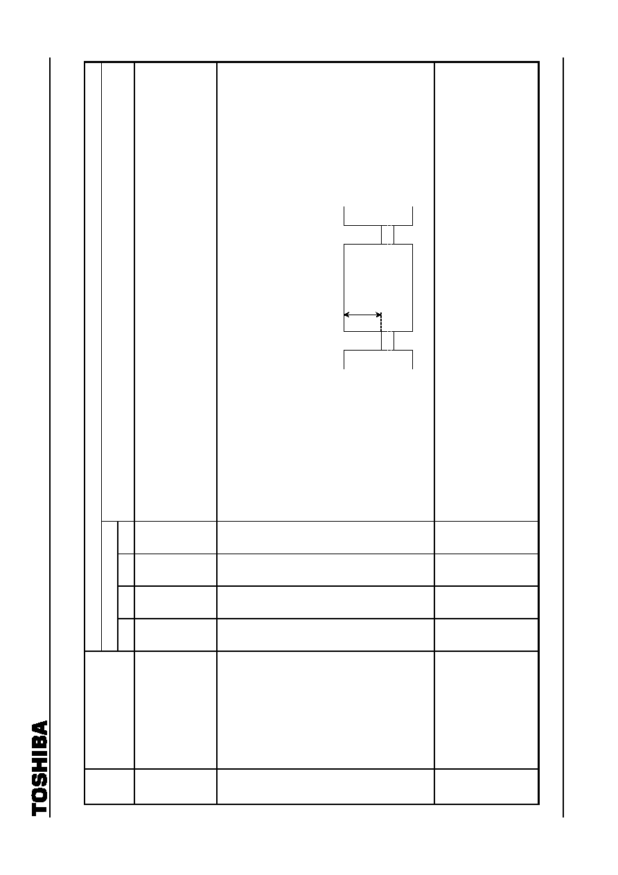
TA1276AFG
2002-04-01
36
Test Conditions
Test Conditions (unless otherwise stated, V
CC1
=
5 V, V
CC2
/V
CC3
/DEF V
CC
=
9 V, Ta
=
25
±
3∞C)
Switching Mode
Note Parameter
SW
15
SW
49
SW
50
SW
53
Test Conditions
Video
Block
Video block common test conditions
1) SW
13
: A, SW
18
: ON, SW
20
: ON, SW
23
: ON, SW
33
: A, SW
34
: A, SW
35
: A, SW
37
: A, SW
38
: A, SW
39
: A, SW
46
: ON,
SW
51
: B, SW
52
: B
2) For testing, see the picture sharpness AC characteristics testing circuit diagram. After using the preset values to
transmit the BUS control data, set ACB operation switching to ACB off (01).
3) Ensure the composite signal is always input to pin 52 (Y
1
/sync input).
V
1
Black
Detect
Level
Shift
C OFF C
C
1) Set the BUS control data to the preset value.
2) Connect pin 78 to an external power supply (PS) and observe pin 2.
3) Turn the Y mute off (1), turn the black stretch gain off (1), and set the black detect level to 0 IRE (1).
4) Increase the PS voltage from 5 V and measure the DC differential VB of pin 3 where the picture period (high period) of
pin 2 goes low.
5) Set the black detect level to 3 IRE (0).
6) As in 4), measure the DC differential VB3 of pin 3.
V
2
Black Stretch Amp Maximum
Gain
A
A
1) Set the BUS control data to the preset value.
2) Set SW50 to A (maximum gain) and input a 500 kHz sine wave to TP78.
3) Use pin 78 to adjust the signal amplitude to 0.1 V
p-p
.
4) Turn the Y mute off (1), turn the black stretch gain off (1), and measure the amplitude VA of pin 3.
5) Turn the black stretch gain on (0) and measure the amplitude VB of pin 3.
6) Calculate
the
G
BS
using the following formula.
G
BS
=
VB
˜
VA
Pin 38
V
B
.V
B3
Pin 3
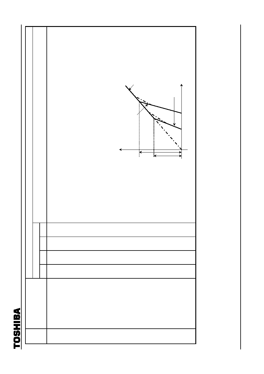
TA1276AFG
2002-04-01
37
Test Conditions (unless otherwise stated, V
CC1
=
5 V, V
CC2
/V
CC3
/DEF V
CC
=
9 V, Ta
=
25
±
3∞C)
Switching Mode
Note Parameter
SW
15
SW
49
SW
50
SW
53
Test Conditions
V
3
Black Stretch Start Point (1)
C
OFF
A
C
1) Set the BUS control data to the preset value.
2) Set
SW
50
to A (maximum gain), turn the Y mute off (1), and turn the black stretch gain off.
3) Connect pin 78 to an external power supply (PS), increase the voltage from V
53
, and plot the resulting change in
voltage S
1
of pin 3.
4) Next, turn the black stretch gain on (0), set the black stretch point 1 to the minimum (000), increase the PS voltage
from V
53
as in 3), and plot the resulting change in voltage S
2
of pin 3.
5) Set the black stretch point 1 to the maximum (111), increase the PS voltage from V
53
as in 3), and plot the change in
voltage S
3
of pin 3.
6) Use the diagram below to calculate the intersections V
BST1
and V
BST2
of S
1
, S
2
, and S
3
. Use the following formulas
to calculate P
BST1
and P
BST2
.
P
BST1
[(IRE)]
=
((V
BST1
[V]
-
V
49
[V]
˜
1.4 [V])
◊
100 [(IRE)]
P
BST2
[(IRE)]
=
((V
BST2
[V]
-
V
49
[V]
˜
1.4 [V])
◊
100 [(IRE)]
Pin
V
49
V
BST2
S
2
(asymptotic line)
S
1
V
BST1
Pin
S
3
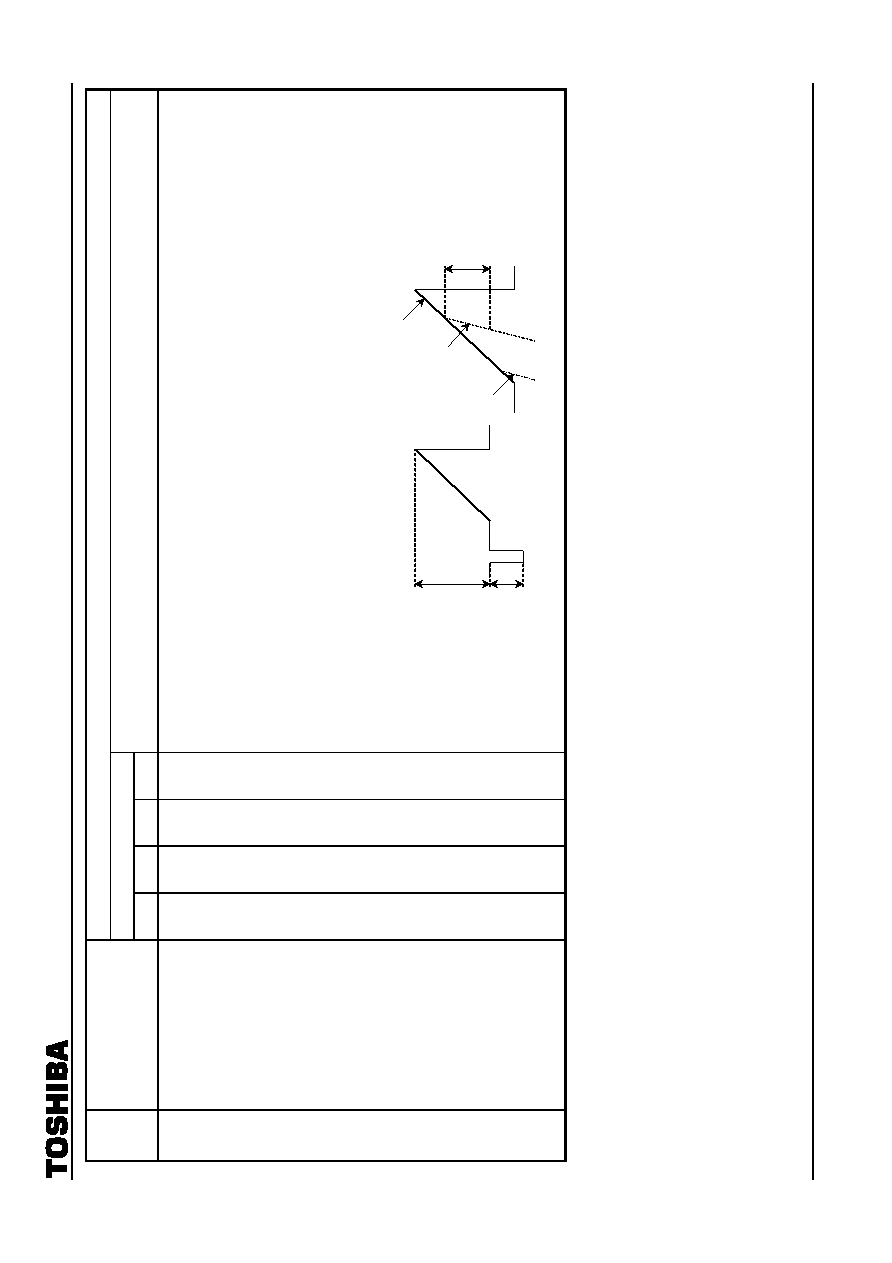
TA1276AFG
2002-04-01
38
Test Conditions (unless otherwise stated, V
CC1
=
5 V, V
CC2
/V
CC3
/DEF V
CC
=
9 V, Ta
=
25
±
3∞C)
Switching Mode
Note Parameter
SW
15
SW
49
SW
50
SW
53
Test Conditions
V
4
Black Stretch Start Point (2)
C
ON
A
A
1) Set the BUS control data to the preset value.
2) Turn the black stretch gain off (1), turn the Y mute off (1), and turn the video mute off (0).
Input the TG7 linearity to TP53, use pin 78 to adjust the amplitude as in the diagram, set unicolor to the center
(1000000), and measure the resulting amplitude (V
43
) of pin 11 (R OUT).
3) Turn the black stretch gain on (0), connect pin 3 to an external power supply (PS), and measure pin 11 (R OUT).
4) When the black stretch start point 2 data are at the minimum (000), calculate as in the diagram the black stretch start
point differential
V
000
for when P is V
49
(APL 0%) and for when P is V
49
+
1.0 [V] (APL 100%).
5) Next, when the black stretch start point 2 data are maximum (111), calculate differential
V
111
in the same way.
6) Calculate the following formulas.
P
BS1
=
(
V
000/
V
43
)
◊
100
P
BS2
=
(
V
111
/V
43
)
◊
100
V
***
0.7 V
p-p
0.3 V
p-p
Pin 78 waveform
Pin 11 (R
APL 0%
APL 100%
LINEARITY
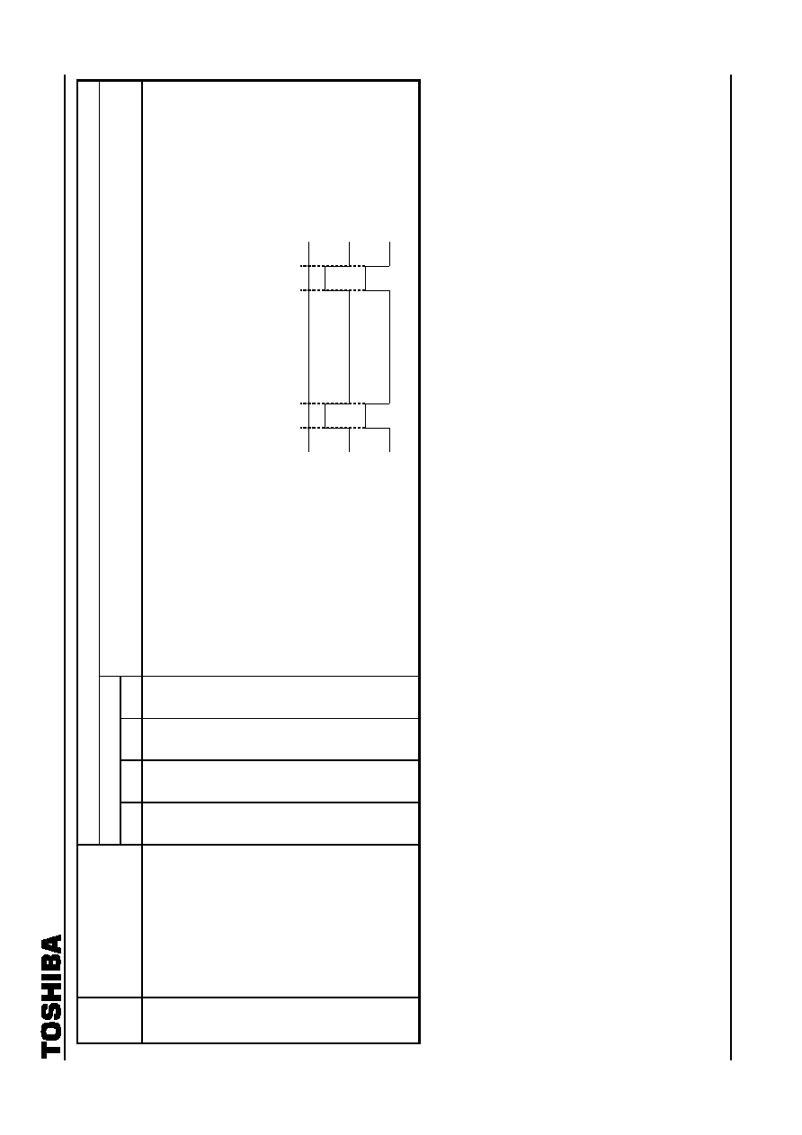
TA1276AFG
2002-04-01
39
Test Conditions (unless otherwise stated, V
CC1
=
5 V, V
CC2
/V
CC3
/DEF V
CC
=
9 V, Ta
=
25
±
3∞C)
Switching Mode
Note Parameter
SW
15
SW
49
SW
50
SW
53
Test Conditions
V
5
D.ABL Detect Voltage
C
OFF
A
C
1) Set the BUS control data to the preset value.
2) Turn the Y mute off (1), set the ABL sensitivity to the minimum (000), set the D.ABL sensitivity to the maximum (111),
and turn the black stretch gain off (1).
3) Connect pin 8 to an external power supply (PS) and decrease the voltage from 6.5 V.
4) Repeat 3) when the D.ABL detect voltage bus data are 000, 001, 010, and 100 respectively. Measure PS voltages
V
000
, V
001
, V
010
, and V
100
when the picture period of pin 3 changes to low. (enlarge the range before measuring.)
5) Next, calculate the
V
001
,
V
010
, and
V
100
voltage differentials from V
000
and V
001
, V
010
, and V
100
.
V
***
=
V
000
-
V
001
(V
010
, V
100
)
Pin 38
Pin 3 Detected
Pin 3 Undetected
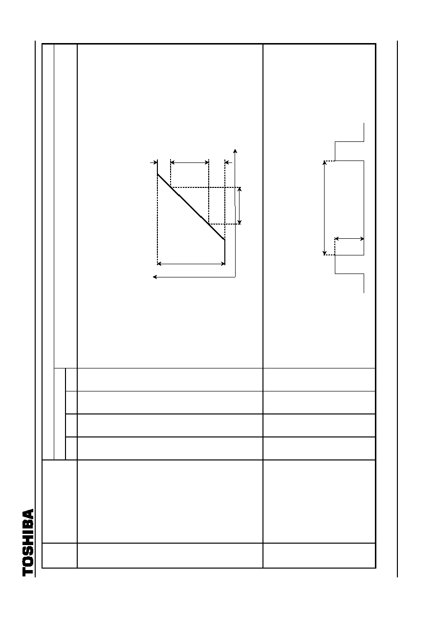
TA1276AFG
2002-04-01
40
Test Conditions (unless otherwise stated, V
CC1
=
5 V, V
CC2
/V
CC3
/DEF V
CC
=
9 V, Ta
=
25
±
3∞C)
Switching Mode
Note Parameter
SW
15
SW
49
SW
50
SW
53
Test Conditions
V
6
D.ABL
Sensitivity
C ON A C
1) Set the BUS control data to the preset value.
2) Turn the Y mute off (1), turn the black stretch gain off (1), and connect pin 8 to an external power supply.
3) With the D.ABL detect voltage at the minimum (000), plot the voltage characteristics of pin 3 in relation to the voltage
of pin 8 when D.ABL sensitivity is at the minimum (000) and the maximum (111).
4) From the diagram, calculate the S
DAMIN
and S
DAMAX
gradients.
S
DAMIN
, S
DAMAX
=
Y/
X
V
7
Black
Level
Compensation
OFF
1) Set the BUS control data to the preset value.
2) Turn the Y mute off (1), turn the black stretch gain off (1), and observe pin 3.
3) Turn the black level compensation on (1), measure
V
1
[mV], and calculate the following formula.
B
LC
=
(
V
1
/1.4
◊
10
3
)
◊
100 (IRE)
Pin 8
Pin 3
Y
10%
10%
100%
X
V
1
[mV]
Picture period
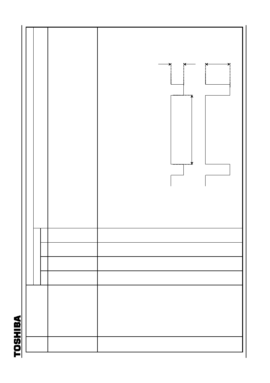
TA1276AFG
2002-04-01
41
Test Conditions (unless otherwise stated, V
CC1
=
5 V, V
CC2
/V
CC3
/DEF V
CC
=
9 V, Ta
=
25
±
3∞C)
Switching Mode
Note Parameter
SW
15
SW
49
SW
50
SW
53
Test Conditions
V
8
Black Peak Detect Level
C
ON
C
C
1) Set the BUS control data to the preset value.
2) Measure the DC voltage V
49
of pin 3.
3) Connect pin 78 to an external power supply (PS).
4) Turn the Y mute off (1), the black stretch gain off (1), and set the black detect level shift to 0 IRE (1).
5) Increase the PS from 0 V and measure the voltage V
BP
of pin 3 where the DC level of the picture period of pin 2 shifts
from high to low.
6) Calculate
V
BP
from the following formula.
V
BP
=
V
BP
-
V
49
V
9
DC Transmission Rate
Compensation Gain
B
1) Set the BUS control data to the preset value.
2) Turn the Y mute off (1), turn the video mute off (0), and connect pin 78 to an external power supply (PS).
3) Measure the amplitude V
43
of pin 11, set the PS to V
53
+
0.7 V, and adjust V
43
to 0.7 V
p-p
using unicolor.
4) With the DC transmission rate compensation gain at the minimum (000), measure
V
1
and
V
2
as in the diagram
below.
5) Next, with the DC transmission rate compensation gain at the maximum (111), measure
V
3
and
V
4
.
6) Calculate ADT100 and ADT130 from the following formula.
ADT100
=
(
V
2
[V]
-
V
1
[V])
˜
0.1 [V]
ADT130
=
(
V
4
[V]
-
V
3
[V])
˜
0.1 [V]
Picture period
V
1
(
V
3
)
V
53
+
0.1 [V]
V
2
(
V
4
)
Pin 11 waveform
V
53
+
0.2 [V]
TA1276AFG
2002-04-01
42
Test Conditions (unless otherwise stated, V
CC1
=
5 V, V
CC2
/V
CC3
/DEF V
CC
=
9 V, Ta
=
25
±
3∞C)
Switching Mode
Note Parameter
SW
15
SW
49
SW
50
SW
53
Test Conditions
V
10
DC Transmission
Compensation Start Point
C ON B C
1) Repeat steps 1) and 2) of V
21
.
2) Measure the amplitude V
43
of pin 11, set the PS to V
53
+
0.7 V, and adjust V
43
to around 1.0 V
p-p
using unicolor.
3) With the DC transmission compensation rate at the minimum (000), increase PS from V
53
and plot the relationship
between the voltages of pins 3 and 11.
4) Next, with the DC transmission compensation rate at the maximum (111), increase PS from V
53
and plot the
relationship between the voltages of pins 3 and 11.
5) With the DC transmission compensation rate at the maximum (111), increase the PS from V
53
when the DC
transmission compensation start point reaches the maximum (111) and plot the relationship between the voltages of
pins 3 and 11.
6) Calculate
V
DT0
and V
DT42
from the following formula.
V
DT0
=
((V
SP0
-
V
49
)/1 [V])
◊
100 [%]
V
DT42
=
((V
SP42
-
V
49
)/1 [V])
◊
100 [%]
Pin
V
PC
DC transmission compensation rate 000
VSP0
Pin
VSP42
DC transmission
compensation start point
DC transmission
compensation start point
TA1276AFG
2002-04-01
43
Test Conditions (unless otherwise stated, V
CC1
=
5 V, V
CC2
/V
CC3
/DEF V
CC
=
9 V, Ta
=
25
±
3∞C)
Switching Mode
Note Parameter
SW
15
SW
49
SW
50
SW
53
Test Conditions
V
11
DC Transmission
Compensation Limit Point
C ON B C
1) Set the BUS control data to the preset value.
2) Turn the Y mute off (1), turn the video mute off (0), and with the unicolor set at maximum (1111111), connect pin 3 to
an external power supply (PS).
3) Set the DC transmission compensation rate to the maximum (111).
4) Increase the PS from 5 V, observe pin 11, and plot the DC transmission compensation rate.
5) Repeat 4) above but change the DC transmission compensation limit point data. Calculate P
DTL60
, P
DTL73
, P
DTL87
,
and P
DTL100
from the measured data and the following formulas.
P
DTL60
=
((V
L60
-
V
49
)/1.0)
◊
100 [%]
P
DTL73
=
((V
L73
-
V
49
)/1.0)
◊
100 [%]
P
DTL87
=
((V
L87
-
V
49
)/1.0)
◊
100 [%]
P
DTL100
=
((V
L100
-
V
49
)/1.0)
◊
100 [%]
Pin
V
L100
Pin
100% (00)
V
L73
V
L87
V
L60
87% (01)
73% (10)
60% (11)
TA1276AFG
2002-04-01
44
Test Conditions (unless otherwise stated, V
CC1
=
5 V, V
CC2
/V
CC3
/DEF V
CC
=
9 V, Ta
=
25
±
3∞C)
Switching Mode
Note Parameter
SW
15
SW
49
SW
50
SW
53
Test Conditions
V
12
Picture Sharpness Control
Range
C OFF B A
1) Set the BUS control data to the preset value.
2) Input a sine wave to TP78.
3) Set the amplitude of pin 78 to 20 mV
p-p
.
4) Set the unicolor to the maximum (1111111), set SHR tracking to SRT-gain low (11), and set the aperture compensator
peak frequency to 4.2M (001).
5) Turn the Y mute off (1), the video mute off (0), connect TP11 and TP15b, and observe TP15a.
6) Set the picture sharpness to the maximum (1111111). When the frequencies are 100 kHz and F
APL01
, measure the
V
100
and V
L
amplitudes respectively and calculate G
MAXL
by the formula shown below.
7) Next, set the picture sharpness to the minimum (0000000). As in 6), when the frequencies are 100 kHz and 2.4 MHz,
measure the V
100
and V
L
amplitudes respectively and calculate G
MINL
by the formula shown below.
8) Set the aperture compensator peak frequency to 7.7M (111) and the picture sharpness to the maximum (1111111).
When the frequencies are 100 kHz and F
APH11
, measure the V
100
and V
H
amplitudes respectively and calculate
G
MAXH
by the formula shown below.
9) Next, set the picture sharpness to the minimum (0000000). When the frequencies are 100 kHz and 4 MHz, measure
the V
100
and V
H
amplitudes respectively and calculate G
MINH
by the following formula.
G
****
[dB]
=
20
◊
Log (V
L (H)
˜
V
100
)
V
13
YNR
Characteristics
1) Repeat steps 1) to 5) of V
12
.
2) With YNR on (1) and the picture sharpness at minimum (0000000), measure the TP15a amplitudes V
100
and V
L
when
the input signal frequencies are 100 kHz and 2.4 MHz respectively.
3) Next, set the aperture compensator peak frequency to 7.7M (111). When the input signal frequencies are 100 kHz and
4 MHz, measure the V
100
and V
H
amplitudes respectively and calculate G
YL
and G
YH
by the following formula.
G
YL (H)
[dB]
=
20
◊
Log (V
L (H)
˜
V
100
)
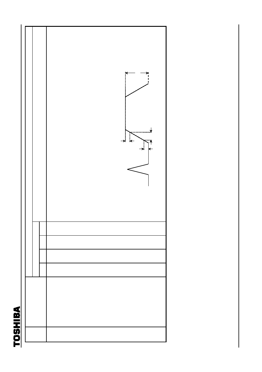
TA1276AFG
2002-04-01
45
Test Conditions (unless otherwise stated, V
CC1
=
5 V, V
CC2
/V
CC3
/DEF V
CC
=
9 V, Ta
=
25
±
3∞C)
Switching Mode
Note Parameter
SW
15
SW
49
SW
50
SW
53
Test Conditions
V
14
2T Pulse Response SRT
Control
C ON B A
1) Set the BUS control data to the preset value.
2) Input a 2T pulse (STD) signal to TP78, turn the Y mute off (1), turn the video mute off (0), set unicolor to maximum
(1111111), and set SHR tracking to SRT-gain low (11).
3) Set the sharpness control to the center (1000000), set the aperture compensator peak frequency to 4.2M (001),
connect TP11 and TP15b, and observe TP15a.
4) Measure
T
SL1
as in the diagram below.
5) Set SHR tracking to SRT-gain high (00) and measure T
SL2
.
6) Next, set the aperture compensator peak frequency to 7.7M (111) and measure T
SH1
and T
SH2
as above.
7) Calculate the following formula.
T
SRTL
=
T
SL1
-
T
SL2
T
SRTH
=
T
SH1
-
T
SH2
100%
10%
10%
T
S
**
TA1276AFG
2002-04-01
46
Test Conditions (unless otherwise stated, V
CC1
=
5 V, V
CC2
/V
CC3
/DEF V
CC
=
9 V, Ta
=
25
±
3∞C)
Switching Mode
Note Parameter
SW
15
SW
49
SW
50
SW
53
Test Conditions
V
15
VSM
Gain
C ON B A
1) Set the BUS control data to the preset value.
2) Input
the
frequency
F
VL
sine wave to TP78.
3) Turn the Y mute off (1), turn the video mute off (0), set the aperture compensator peak frequency to 4.2M (001), and
set the amplitude of pin 78 to 0.1 V
p-p
.
4) Measure the TP5 amplitudes V
L00
, V
L01
, V
L10
, and V
L11
in the following cases.
VSM gain
0dB
(00)
V
L (H) 00
-
6dB (01)
V
L (H) 01
-
9dB (10)
V
L (H) 10
OFF
(11)
V
L (H) 11
5) Input the sine wave of frequency F
VH
to TP78, set the aperture compensator peak frequency to 7.7M (111), and
measure the TP5 amplitudes V
H00
, V
H01
, V
H10
, and V
H11
as above.
6) Calculate the following formulas.
G
VL (H) 00
=
20
◊
Log (V
L (H) 00
/0.1) [dB]
G
VL (H) 01
=
20
◊
Log (V
L (H) 01
/0.1) [dB]
-
20
◊
Log (V
L (H) 00
/0.1) [dB]
G
VL (H) 10
=
20
◊
Log (V
L (H) 10
/0.1) [dB]
-
20
◊
Log (V
L (H) 00
/0.1) [dB]
G
VL (H) 11
=
20
◊
Log (V
L (H) 00
/0.1) [dB]
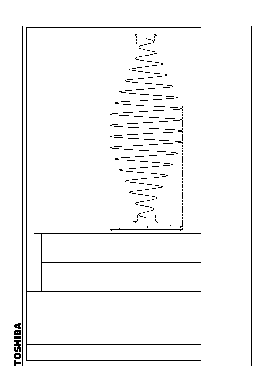
TA1276AFG
2002-04-01
47
Test Conditions (unless otherwise stated, V
CC1
=
5 V, V
CC2
/V
CC3
/DEF V
CC
=
9 V, Ta
=
25
±
3∞C)
Switching Mode
Note Parameter
SW
15
SW
49
SW
50
SW
53
Test Conditions
V
16
VSM Horizontal Parabola
Modulation Gain
C ON B A
1) Repeat steps 1) to 3) of V
15
.
2) Turn on the VSM output horizontal parabola modulation (1) and set the VSM gain to 0dB (00).
3) As in the diagram, measure the picture period amplitudes VCL, VRL, and VLL of TP5.
4) Next, input the sine wave of frequency F
VH
to TP78, set the aperture compensator peak frequency to 7.7M (111), set
the VSM horizontal parabola frequency to 31.5k (10), and measure the picture period amplitudes VCH, VRH, and VLH
of TP5 as above.
5) Calculate
G
VRL
, G
VLL
, G
VRH
, and G
VLH
from the following formulas.
G
VRL (H)
=
20
◊
Log (VRL (H)/VCL (H))
G
VLL (H)
=
20
◊
Log (VLL (H)/VCL (H))
6) In 3) and 4) above, turn the VSM output horizontal parabola modulation off (0) and check that no parabola modulation
is generated on the picture period signal. (VPOFL, VPOFH)
50%
VCL (H)
VLL (H)
VRL (H)

TA1276AFG
2002-04-01
48
Test Conditions (unless otherwise stated, V
CC1
=
5 V, V
CC2
/V
CC3
/DEF V
CC
=
9 V, Ta
=
25
±
3∞C)
Switching Mode
Note Parameter
SW
15
SW
49
SW
50
SW
53
Test Conditions
V
17
VSM High-Speed Mute
Response Time
C ON B A
1) Repeat steps 1) to 3) of V
15
, then observe pin 5.
2) Input a pulse like that shown below to pin 27 and measure the response time T
VML1
(2) at that input.
3) Similarly, input the pulse to pin 21 and measure the response time T
VML3
(4) at that input.
4) Input the sine wave of frequency F
VH
to TP78, set the aperture compensator peak frequency to 7.7M (111), and
measure the response time T
VMH1
(2) as in 2) above.
5) Similarly, input the pulse to pin 21 and measure the response time T
VMH3
(4) at the input.
Square wave (50 kHz, 2 V
p-p
)
Mute time
T
VML2
(4), T
VMH2
(4)
T
VML1
(3), T
VMH1
(3)
Pin 5 Waveform
2 [V]
0 [V]
V
SR36
[V]
Pin 27 (pin)
TA1276AFG
2002-04-01
49
Test Conditions (unless otherwise stated, V
CC1
=
5 V, V
CC2
/V
CC3
/DEF V
CC
=
9 V, Ta
=
25
±
3∞C)
Subaddress Switching
Mode
Note Parameter
07 10 17 18 SW
5
SW
6
SW
13
SW
15
Test Conditions
Chroma
Block
Chroma block common test conditions
SW
13
: B, SW
15
: C, SW
18
: ON, SW
20
: ON, SW
23
: ON, SW
24
: ON, SW
25
: ON,
SW
33
: A, SW
34
: A, SW
35
: A, SW
37
: A, SW
38
: A, SW
39
: A, SW
46
: ON
C
1
ACC
Characteristics
80 00 00 00 OPEN
OPEN B
A
1) Input 3.58-NTSC rainbow signal (C-4 signal) burst/chroma signals with the same
burst/chroma amplitude to the chroma input pin (TP54).
2) Measure the output amplitudes F
10
, F
30
, F
300
, and F
600
of the UQ output pin 65
when the chroma input amplitude levels are set to 10, 30, 300, and 600 mV
p-p
.
3) Calculate
A
=
F
30
/F
300
.
C
2
APC Frequency Control
Sensitivity
A
1) Connect
SW
13
to A.
2) Switch the color system mode (10) to 3.58 NTSC (00), 4.43 PAL (60), and M-PAL
(80) and measure the following for each of those cases.
3) Connect external voltage source (V
11
) to APC filter pin 58.
4) Vary the voltage of the external voltage source (V
11
) and observe the f
sc
output pin
72 using a frequency counter.
5) Measure
the
free-run
sensitivity
for the V
11
+
V
11
(100 mV) near the f
c
.
(3.5 NTSC
=
3
, 4.3; PAL
=
4
; M-PAL
=
M
)
C
3
APC Pull-In and Hold Range
1) Input 3.579545 MHz, 4.433619 MHz, and 3.575611 MHz continuous waves (200
mV
p-p
to the chroma input pin (TP54).
2) Switch the color system mode (10) to 3.58 NTSC (00), 4.43 PAL (60), and M-PAL
(80), and measure the following for each of those cases.
3) Vary the input signal frequency in 10 Hz-steps within a range of
±
3 kHz.
4) Clamp
B/W
color mode (f
*
P
*
). While holding color
B/W mode (f
*
H
*
),
measure the
±
deviations from the frequency at each continuous wave input.
C
4
SECAM Output DC Level
Change
C
0
00
or
30
or
60
1) Connect
SW
13
to A.
2) Measure the output DC level of the SECAM control pin 3 when the color system
mode (10) is switched to 3.58 NTSC (00), 4.43 PAL (30), and SECAM (60).
(3.58 NTSC mode: SEN)
(4.43 PAL mode: SEP)
(SECAM mode: SES)
TA1276AFG
2002-04-01
50
Test Conditions (unless otherwise stated, V
CC1
=
5 V, V
CC2
/V
CC3
/DEF V
CC
=
9 V, Ta
=
25
±
3∞C)
Subaddress Switching
Mode
Note Parameter
07 10 17 18 SW
5
SW
6
SW
13
SW
15
Test Conditions
C
5
NTSC
Ident
Sensitivity
80
C
0
or
D
0
00 00
OPEN
OPEN
B A
1) Input a 3.58-NTSC rainbow (C-4 signal) burst/chroma signal with the same
burst/chroma amplitudes to the chroma input pin (TP54).
2) Observe the BUS READ mode (5
th
and 6
th
bits of the 1
st
byte).
3) Switch the Indent sensitivity (set the subaddress (10) data low (C
0
) and high (D
0
))
and perform the following measurements.
4) Increase the input signal amplitude from 0 and measure the input signal amplitude
at the switch to 3.58 NTSC mode.
(LOW (C
0
): vN
CL
, High (D
0
): vN
CH
)
5) Lower the input signal amplitude from 100 mV
p-p
and measure the input signal
amplitude at the deviation from 3.58 NTSC mode.
(LOW (C
0
): vN
BL
, High (D
0
): vN
BH
)
C
6
PAL
Ident
Sensitivity
1) Input a 4.43-PAL rainbow (C-4 signal) burst/chroma signal with the same
burst/chroma amplitude to the chroma input pin (TP54).
2) Observe the BUS READ mode (5
th
and 6
th
bits of the 1
st
byte).
3) Switch the Indent sensitivity (set the subaddress (10) data low (C
0
) and high (D
0
))
and perform the following measurements.
4) Increase the input signal amplitude from 0 and measure the input signal amplitude
at the switch to 4.43 PAL mode.
(LOW (C
0
): vP
CL
, High (D
0
): vP
CH
)
5) Lower the input signal amplitude from 100 mV
p-p
and measure the input signal
amplitude at the deviation from 4.43 PAL mode.
(LOW (C
0
): vP
BL
, High (D
0
): vP
BH
)
C
7
TOF
Characteristics
00
or
60
38
1) Input the signal C-1 to the chroma input pin (TP54).
(signal amplitude
=
50 mV
p-p
).
2) When the subaddress (10) data are f
0
=
3.58 MHz (00) and f
0
=
4.43 MHz (60), and
subaddress (18) data are (38), connect 1.5 k
between the V
I
output pin 6 and the
5 V-V
CC
and observe the V
I
output pin 64.
3) Measure the output amplitude when f
0
=
3.58 MHz and calculate the gain in
decibels from the input (GF
C3
).
4) Measure the output amplitude when f
0
=
3.58 MHz
±
500 kHz and calculate the
gain in decibels from the input
(
+
500 kHz: GF
H3
,
-
500 kHz: GF
L3
).
5) Measure the output amplitude when f
0
=
4.43 MHz and calculate the gain in
decibels from the input (GF
C4
).
6) Measure the output amplitude when f
0
=
4.43 MHz
±
500 kHz and calculate the
gain in decibels from the input
(
+
500 kHz: GF
H4
,
-
500 kHz: GF
L4
).
TA1276AFG
2002-04-01
51
Test Conditions (unless otherwise stated, V
CC1
=
5 V, V
CC2
/V
CC3
/DEF V
CC
=
9 V, Ta
=
25
±
3∞C)
Switching Mode
Note Parameter
SW
33
SW
34
SW
35
SW
37
SW
38
SW
39
SW
51
SW
52
SW
53
Test Conditions
Text Block
Text block common test conditions
SW
13
: A, SW
15
: C, SW
18
: ON, SW
20
: ON,
SW
23
: ON, SW
24
: ON, SW
25
: ON
T
1
AC
Gain
A A A A A A B B A
1) Input
signal
1
(f
0
=
100 kHz, picture period amplitude
=
0.2 V
p-p
) to pin 78.
2) Measure the picture period amplitude of pins 15, 13, 11 (V41, V42, and
V43).
3) G
R
=
V43/0.2
G
G
=
V42/0.2
G
B
=
V41/0.2
T
2
Unicolor Adjustment
Characteristics
1) Input
signal
1
(f
0
=
100 kHz, picture period amplitude
=
0.2 V
p-p
) to pin 78.
2) Set the unicolor data to maximum (7F), center (40), and minimum (00) and
measure the pin 11 picture period amplitudes for each case.
(v
u
MAX, v
u
CNT, v
u
MIN)
3) Calculate the unicolor maximum and minimum amplitude ratios using
digital conversion. (
v
u
)
T
3
Brightness Adjustment
Characteristics
1) Input signal 2 to pin 78 and adjust the picture period amplitude output of
pin 11 to 1 V
p-p
.
2) Measure the voltage of pin 11 when the brightness is changed to
maximum (FF), center (80), and minimum (00). (VbrMAX, VbrCNT,
VbrMIN)
T
4
Brightness
Sensitivity
1) Using the results obtained from T
3
, calculate the brightness sensitivity
from the following formula.
2) Gbr
=
(VbrMAX
-
VbrMIN)/256
T
5
White Peak Slice Level
1) Change the bus data and set the sub-contrast to maximum.
2) Connect an external power supply to pin 78 and increase the voltage
gradually from 5.8 V.
3) Measure the picture period amplitude voltage of pin 11 when pin 11∞s
picture period is clipped (Vwps1).
4) Change the subaddress (05) data to (81) and repeat steps 1) to 3) above.
(Vwps2)
T
6
Black Peak Slice Level
C
1) Repeat step 1) of T
5
.
2) Connect an external power supply to pin 78 and decrease the voltage
gradually from 5.8 V.
3) Measure the voltages of pins 11, 13, and 15 when their picture periods are
clipped.
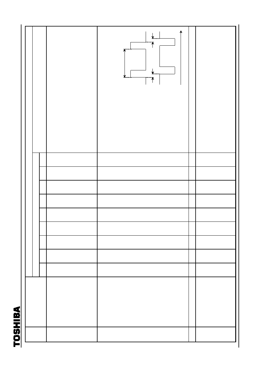
TA1276AFG
2002-04-01
52
Test Conditions (unless otherwise stated, V
CC1
=
5 V, V
CC2
/V
CC3
/DEF V
CC
=
9 V, Ta
=
25
±
3∞C)
Switching Mode
Note Parameter
SW
33
SW
34
SW
35
SW
37
SW
38
SW
39
SW
51
SW
52
SW
53
Test Conditions
T
7
Half
Tone
Characteristics A A A A A A B B A
1) Input
signal
1
(f
0
=
100 kHz, picture period amplitude
=
0.2 V
p-p
) to pin 78.
2) Measure the picture period amplitude of pin 15 (V41
A
).
3) Apply 1.5 V from an external power supply to pin 6.
4) Measure the picture period amplitude of pin 15 (V41
B
).
5) G
HT1
=
V41
B
/V41
A
6) Halt the voltage applied to pin 6, set the subaddress (03) data to (81), and
measure the picture period amplitude of pin 15 (V41
C
).
7) G
HT2
=
V41
C
/V41
A
T
8
BLK
Pulse
Delay
Time
C
1) Calculate
t
dON
, t
dOFF
from the signal applied to pin 25 (H.BLK input) (A
below) and the output signals from pins 11, 13, and 15 (B below).
(A) Signal applied to pin 25
(B) Output signals from pins
11, 13, 15
T
9
RGB
Output
Voltage
1) Measure the picture period voltages for pins 11, 13, and 15.
T
10
Cutoff Voltage Variable
Range
1) Set the subaddress (17) data to (07).
2) Measure the picture period voltage of pin 11 when the cutoff (subaddress
0C) data are changed to maximum (FF), center (80), and minimum (00),
and calculate the amount of change of maximum and minimum from the
center. (CUT
+
, CUT
-
).
3) In steps 1) and 2) above, make the following changes and remeasure:
Change the subaddress (0D) data and measure pin 13,
Change the subaddress (0E) data and measure pin 15.
63.5
µ
s
t
dON
t
dOFF
t
TA1276AFG
2002-04-01
53
Test Conditions (unless otherwise stated, V
CC1
=
5 V, V
CC2
/V
CC3
/DEF V
CC
=
9 V, Ta
=
25
±
3∞C)
Switching Mode
Note Parameter
SW
33
SW
34
SW
35
SW
37
SW
38
SW
39
SW
51
SW
52
SW
53
Test Conditions
T
11
Drive Adjustment Variable
Range
A A A A A A B B A
1) Input
signal
1
(f
0
=
100 kHz, picture period amplitude
=
0.2 V
p-p
) to pin 78.
2) Measure the picture period amplitude of pin 13 when the drive
(subaddress-09) data are changed to maximum (FE), center (80), and
minimum (00).
3) Calculate the maximum and minimum amplitude ratios for the drive center
using decibel conversion. (DRG
+
, DRG
-
)
4) In steps 1) to 3) above, change the subaddress (0A) data, measure pin 15,
and repeat the calculations. (DRB
+
, DRB
-
)
5) In steps 1) to 3) above, set data of the LSB of subaddress (09) to 1,
measure pin 11, and repeat the calculations. (DRR
+
, DRR
-
)
T
12
Output
Voltage
During
Muting
C
1) Set the subaddress (00) data to (FF).
2) Measure the picture period voltages of pins 11, 13, and 15. (MURD,
MUGD, MUBD)
T
13
Output Voltage at Blue Back
1) Set the subaddress (10) data to (08).
2) Measure the picture period voltages of pins 11 and 13 and the picture
period amplitude of pin 15. (BB
R
, BB
G
, BB
B
)
T
14
ACL
Characteristics
A
1) Input
signal
1
(f
0
=
100 kHz, picture period amplitude
=
0.2 V
p-p
) to pin 78.
2) Measure the picture period amplitude of pin 11 (v
ACL1
).
3) Measure the picture period amplitude of pin 11 when
-
0.5 V DC is applied
to pin 8 from an external power supply. (v
ACL2
)
4) Measure the picture period amplitude of pin 11 when
-
1 V DC is applied to
pin 8 from an external power supply. (v
ACL3
)
5) ACL1
=
-
20
◊
og (v
ACL2
/v
ACL1
)
ACL2
=
-
20
◊
og (v
ACL3
/v
ACL1
)
TA1276AFG
2002-04-01
54
Test Conditions (unless otherwise stated, V
CC1
=
5 V, V
CC2
/V
CC3
/DEF V
CC
=
9 V, Ta
=
25
±
3∞C)
Switching Mode
Note Parameter
SW
33
SW
34
SW
35
SW
37
SW
38
SW
39
SW
51
SW
52
SW
53
Test Conditions
T
15
ABL
Point
A A A A A A B B C
1) Measure the DC voltage of pin 8. (VABL1)
2) Set the subaddress (16) data to (1C).
3) Applying external voltage to pin 8, lower the pin voltage from 6.5 V.
Measure the voltage of pin 8 when the voltage of pin 11 starts to change.
(VABL2)
4) Change the data of subaddress (16) to (3C), (5C), (7C), (9C), (BC), (DC),
and (FC), and repeat step 3) for each of these data. (VABL3, VABL4,
VABL5, VABL6, VABL7, VABL8, VABL9)
5) ABL
P1
=
VABL2
-
VABL1, ABL
P5
=
VABL6
-
VABL1
ABL
P2
=
VABL3
-
VABL1, ABL
P6
=
VABL7
-
VABL1
ABL
P3
=
VABL4
-
VABL1, ABL
P7
=
VABL8
-
VABL1
ABL
P4
=
VABL5
-
VABL1, ABL
P8
=
VABL9
-
VABL1
T
16
ABL
Gain
1) Apply 6.5 V from an external power supply to pin 8.
2) Set the subaddress (16) data to (00). Set the brightness to the maximum.
3) Measure the voltage of pin 11. (VABL10)
4) Apply 4.5 V from an external power supply to pin 8.
5) Change the data of subaddress (16) to (00), (04), (08), (0C), (10), (14),
(18), and (1C), and repeat step 3) for each of these data.(VABL11,
VABL12, VABL13, VABL14, VABL15, VABL16, VABL17, VABL18)
6) ABL
G1
=
VABL11
-
VABL10, ABL
G5
=
VABL15
-
VABL10
ABL
G2
=
VABL12
-
VABL10, ABL
G6
=
VABL16
-
VABL10
ABL
G3
=
VABL13
-
VABL10, ABL
G7
=
VABL17
-
VABL10
ABL
G4
=
VABL14
-
VABL10, ABL
G8
=
VABL18
-
VABL10
T
17
RGB
Output
Mode
1) Adjust the brightness so that the picture period voltage of pin 11 is set to
2.5 V.
2) Set the subaddress (16) data to (01).
3) Measure the picture period voltages of pins 11, 13, and 15.
(V43
R
, V42
R
, V41
R
)
4) Change the subaddress (16) data to (02) and repeat step 3).
(V43
G
, V42
G
, V41
G
)
5) Change the subaddress (16) data to (03) and repeat step 3).
(V43
B
, V42
B
, V41
B
)
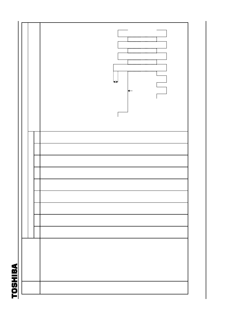
TA1276AFG
2002-04-01
55
Test Conditions (unless otherwise stated, V
CC1
=
5 V, V
CC2
/V
CC3
/DEF V
CC
=
9 V, Ta
=
25
±
3∞C)
Switching Mode
Note Parameter
SW
33
SW
34
SW
35
SW
37
SW
38
SW
39
SW
51
SW
52
SW
53
Test Conditions
T
18
ACB Insertion Pulse Phase
and Amplitude
A A A A A A B B
A
or
C
1) Input
signal
1
(f
0
=
100 kHz, picture period amplitude
=
0.2 V
p-p
) to pin 78
and adjust the drive adjustment data so that the picture period amplitudes
of pins 13 and 15 are equal to that of pin 11.
2) Set
SW
53
to C.
3) Measure the voltages of pins 31, 32, and 74. From an external power
supply, apply the measured voltages to these pins.
4) Set subaddress (15) data to (D
2
).
5) From pins 11, 13, and 15, calculate the phase of the ACB insertion pulse
in accordance with Figure 2 below.
Note 5: After the completion of V.BLK, the video period following the falling
edge of the FBP input is regarded as 1H and the periods at each
completion of H.BLK are counted as 2H, 3H, 4H∑∑∑.
6) Measure the ACB insertion pulse amplitude (the level from the picture
period amplitude at no input) of pins 11, 13, and 15.
V.BLK period
1H
ACB insertion pulse amplitude
2H 3H 4H
Figure 2 RGB Output
Figure 3 FBP Input
(No.38)
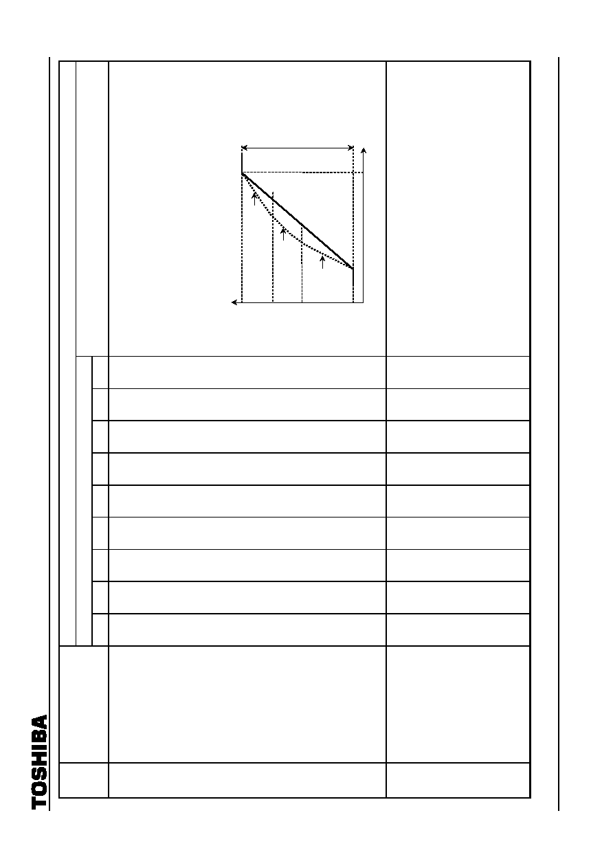
TA1276AFG
2002-04-01
56
Test Conditions (unless otherwise stated, V
CC1
=
5 V, V
CC2
/V
CC3
/DEF V
CC
=
9 V, Ta
=
25
±
3∞C)
Switching Mode
Note Parameter
SW
33
SW
34
SW
35
SW
37
SW
38
SW
39
SW
51
SW
52
SW
53
Test Conditions
T
19
RGB
Characteristics
A A A A A A B B A
1) Input a ramp waveform to pin 78 and adjust the input amplitude so that the
picture period amplitude of pin 11 is 2.3 V
p-p
.
2) Adjust the drive adjustment data so that the picture period amplitudes of
pins 13 and 15 are equal to that of pin 11.
3) Set the subaddress (14) data to (10).
4) From pins 13, 15, and 11, calculate the RGB
start point and its gradient
(decibel conversion) in relation to the off point in accordance with Figure 2.
T
20
Analog RGB Gain
A
or
B
A
or
B
A
or
B
1) Input
signal
1
(f
0
=
100 kHz, picture period amplitude
=
0.2 V
p-p
) to pin 78
and adjust the drive adjustment data so that the picture period amplitudes
of pins 13 and 15 are equal to that of pin 11.
2) Apply 5 V from an external power supply to pin 27.
3) Input
signal
1
(f
0
=
100 kHz, picture period amplitude
=
0.2 V
p-p
) to pin 22.
4) Measure the picture period amplitude of pin 11. (V43
R
)
5) As in steps 2) and 3) above, input to pin 24 and measure pin 13, then input
to pin 25 and measure pin 15. (V42
G
, V41
B
)
6) G
TXR
=
V43
R
/0.2
G
TXG
=
V42
G
/0.2
G
TXB
=
V41
B
/0.2
2.5 V
p-p
100
2
1
(gradient 3)
(gradient 2)
(gradient 1)
Input amplitude
Output amplitude
IRE
TA1276AFG
2002-04-01
57
Test Conditions (unless otherwise stated, V
CC1
=
5 V, V
CC2
/V
CC3
/DEF V
CC
=
9 V, Ta
=
25
±
3∞C)
Switching Mode
Note Parameter
SW
33
SW
34
SW
35
SW
37
SW
38
SW
39
SW
51
SW
52
SW
53
Test Conditions
T
21
Analog RGB White Peak Slice
Level
A A A A A A B B A
1) Repeat step 1) of T
20
.
2) Apply 5 V from an external power supply to pin 27.
3) Set the RGB contrast data to the maximum (7F).
4) Connect an external power supply to pin 22, increase the voltage gradually
from 3.0 V, and measure the picture period amplitude voltage when pin 11
is clipped.
5) As in steps 3) and 4) above, input to pin 24 and measure pin 13, then input
to pin 25 and measure pin 15.
T
22
Analog RGB Black Peak
Limiter Level
1) Repeat step 1) of T
20
.
2) Apply 5 V from an external power supply to pin 27.
3) Set the RGB contrast data to the maximum (7F).
4) Connect an external power supply to pin 22, decrease the voltage
gradually from 4.5 V, and measure the voltage when pin 11 is clipped.
5) As in steps 3) and 4) above, input to pin 24 and measure pin 13, then input
to pin 25 and measure pin 15.
T
23
RGB Contrast Adjustment
Characteristics
A
or
B
A
or
B
A
or
B
1) Repeat step 1) of T
20
.
2) Apply 5 V from an external power supply to pin 27.
3) Input
signal
1
(f
0
=
100 kHz, picture period amplitude
=
0.2 V
p-p
) to pin 22.
4) Measure the picture period amplitude of pin 11 when the RGB contrast
data change to the maximum (7F), the center (40), and the minimum (00).
(vuTXR
MAX
, vuTXR
CNT
, vuTXR
MIN
)
5) Calculate the maximum and minimum amplitude ratios using decibel
conversion. (DRG
+
, DRG
-
)
6) As in steps 3), 4) and 5) above, input to pin 24 and measure pin 13, then
input to pin 25 and measure pin 15.
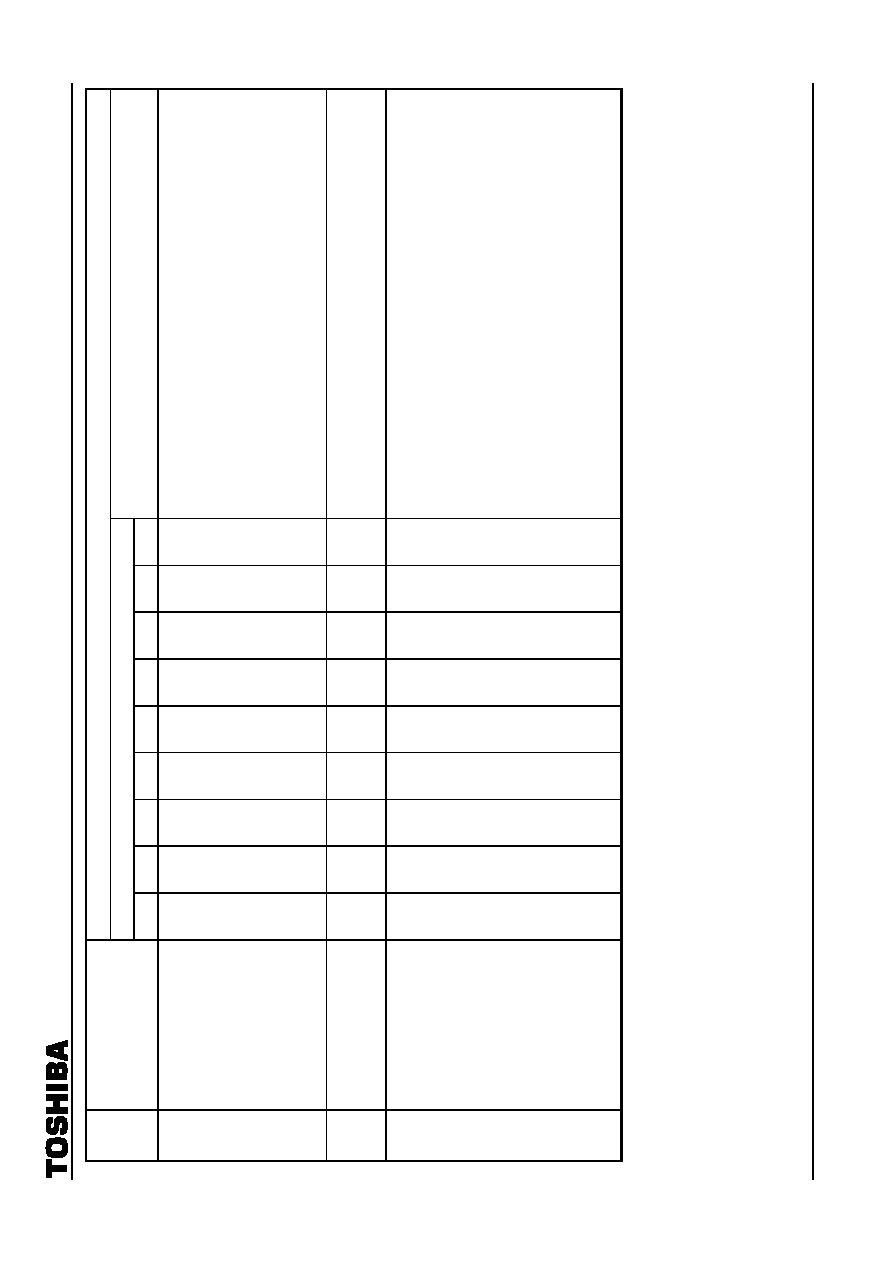
TA1276AFG
2002-04-01
58
Test Conditions (unless otherwise stated, V
CC1
=
5 V, V
CC2
/V
CC3
/DEF V
CC
=
9 V, Ta
=
25
±
3∞C)
Switching Mode
Note Parameter
SW
33
SW
34
SW
35
SW
37
SW
38
SW
39
SW
51
SW
52
SW
53
Test Conditions
T
24
Analog RGB
Brightness Adjustment
Characteristics
A
or
B
A
or
B
A
or
B
A A A B B A
1) Repeat step 1) of T
20
.
2) Input signal 2 to pins 22, 24, and 25.
3) Apply 5 V from an external power supply to pin 27.
4) Adjust the signal 2 amplitude A so that the picture period amplitude of pin
11 is 0.5 V
p-p
.
5) Measure the picture period voltage of pins 11, 13, and 15 when the RGB
brightness change to the maximum (7F), the center (40), and the minimum
(00).
(VbrTX
MAX
, VbrTX
CNT
, VbrTX
MIN
)
T
25
Analog RGB Brightness
Sensitivity
1) Using the results obtained from T24, calculate the RGB brightness
sensitivity for pins 11, 13, and 15.
2) GbrTX
=
(VbrTX
MAX
-
VbrTX
MIN
)/128
T
26
Text
ACL
Characteristics
A
A
B
1) Repeat step 1) of T
20
.
2) Apply 5 V from an external power supply to pin 27.
3) Input
signal
1
(f
0
=
100 kHz, picture period amplitude
=
0.2 V
p-p
) to pin 22.
4) Measure the picture period amplitude of pin 11. (v
TXACL1
)
5) Measure the picture period amplitude of pin 11 when
-
0.5 V DC is applied
to pin 8 from an external source. (v
TXACL2
)
6) Measure the picture period amplitude of pin 11 when
-
1 V DC is applied to
pin 8 from an external source. (v
TXACL3
)
7) TXACL1
=
-
20
◊
og (v
TXACL2
/v
TXACL1
)
TXACL2
=
-
20
◊
og (v
TXACL3
/v
TXACL1
)
8) Set the subaddress (10) data to (01) and repeat the calculations in steps
5) and 6). (TXACL3, TXACL4)
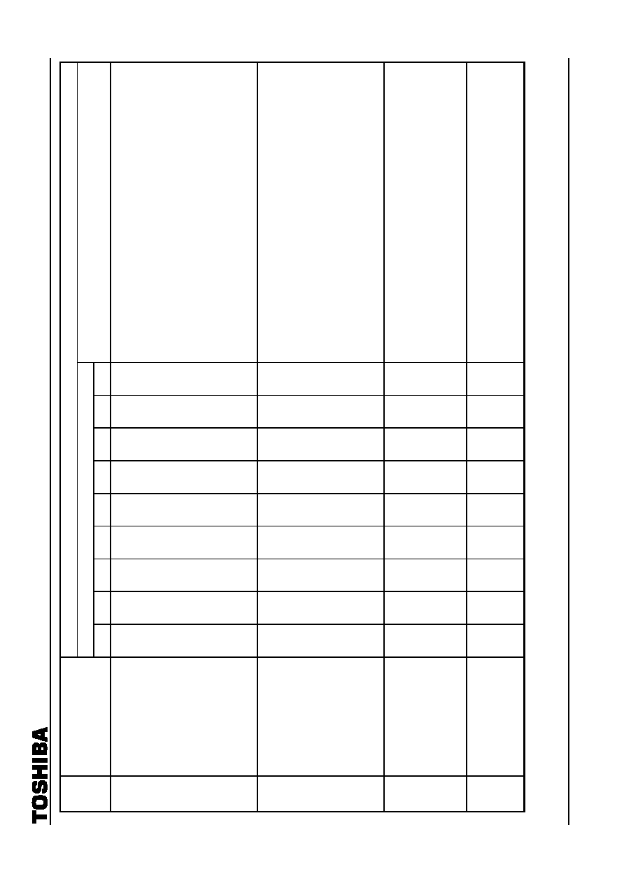
TA1276AFG
2002-04-01
59
Test Conditions (unless otherwise stated, V
CC1
=
5 V, V
CC2
/V
CC3
/DEF V
CC
=
9 V, Ta
=
25
±
3∞C)
Switching Mode
Note Parameter
SW
33
SW
34
SW
35
SW
37
SW
38
SW
39
SW
51
SW
52
SW
53
Test Conditions
T
27
Analog OSD Gain
A
A
A
A
or
B
A
or
B
A
or
B
B B A
1) Input
signal
1
(f
0
=
100 kHz, picture period amplitude
=
0.2 V
p-p
) to pin 78
and adjust the drive adjustment data so that the picture period amplitudes
of pins 13 and 15 are equal to that of pin 11.
2) Apply 5 V from an external power supply to pin 21.
3) Input
signal
1
(f
0
=
100 kHz, picture period amplitude
=
0.2 V
p-p
) to pin 18.
4) Measure the picture period amplitude of pin 11. (V43
R
)
5) As in steps 3) and 4) above, input to pin 19 and measure pin 13, then input
to pin 20 and measure pin 15. (V42
G
, V41
B
)
6) GOSD
R
=
V43
R
/0.2
GOSD
G
=
V42
G
/0.2
GOSD
B
=
V41
B
/0.2
T
28
Analog OSD White Peak Slice
Level
A A A
1) Repeat step 1) of T
27
.
2) Apply 5 V from an external power supply to pin 21.
3) Apply external voltage to pin 18, increase the voltage gradually from 0.0 V,
and measure the picture period amplitude voltage when pin 11 is clipped.
(V
OSD1R
)
4) As in step 3) above, input to pin 19 and measure pin 13. Input to pin 20
and measure pin 15.
5) Set the subaddress (10) data to (04) and repeat the measurements in
steps 3) and 4).
(V
OSD2R
, V
OSD2G
, V
OSD2B
)
T
29
Analog OSD Black Peak
Limiter Level
1) Repeat step 1) of T
27
.
2) Apply 5 V from an external power supply to pin 21.
3) Apply external voltage to pin 18, decrease the voltage gradually from 4.5
V, and measure the voltage when pin 11 is clipped.
4) As in step 3) above, input to pin 19 and measure pin 13. Input to pin 20
and measure pin 15.
T
30
Analog OSD Output DC
Voltage
1) Repeat step 1) of T
27
.
2) Apply 5 V from an external power supply to pin 21.
3) Measure the picture period voltages of pins 11, 13, and 15.
(V
OSDDCR
, V
OSDDCG
, V
OSDDCB
)

TA1276AFG
2002-04-01
60
Test Conditions (unless otherwise stated, V
CC1
=
5 V, V
CC2
/V
CC3
/DEF V
CC
=
9 V, Ta
=
25
±
3∞C)
Switching Mode
Note Parameter
SW
33
SW
34
SW
35
SW
37
SW
38
SW
39
SW
51
SW
52
SW
53
Test Conditions
T
31
OSD
ACL
Characteristics A A A A A B B B A
1) Repeat step 1) of T
27
.
Set the subaddress (10) data to (02).
2) Apply 5 V from an external power supply to pin 21.
3) Input
signal
1
(f
0
=
100 kHz, picture period amplitude
=
0.2 V
p-p
) to pin 18.
4) Measure the picture period amplitude of pin 11. (v
OSDACL1
)
5) Measure the picture period amplitude of pin 11 when
-
0.5 V DC is applied
to pin 8 from an external source. (v
OSDACL2
)
6) Measure the picture period amplitude of pin 11 when
-
1 V DC is applied to
pin 8 from an external source. (v
OSDACL3
)
7) OSDACL1
=
-
20
◊
og (v
OSDACL2
/v
OSDACL1
)
OSDACL2
=
-
20
◊
og (v
OSDACL3
/v
OSDACL1
)
8) Change the subaddress (10) data to (00) and repeat the measurements in
steps 1) to 7). (OSDACL3, OSDACL4)
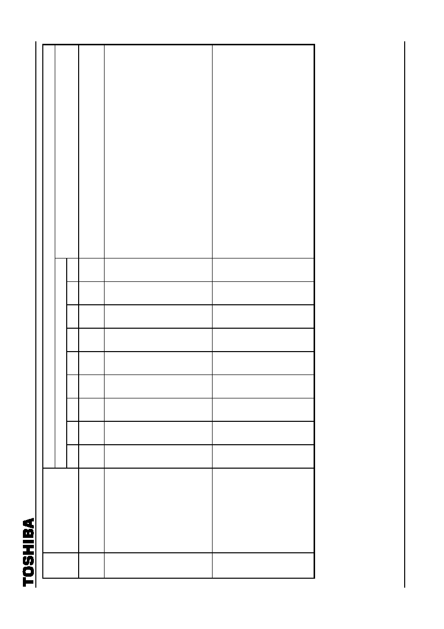
TA1276AFG
2002-04-01
61
Test Conditions (unless otherwise stated, V
CC1
=
5 V, V
CC2
/V
CC3
/DEF V
CC
=
9 V, Ta
=
25
±
3∞C)
Switching Mode
Note Parameter
SW
33
SW
34
SW
35
SW
37
SW
38
SW
39
SW
51
SW
52
SW
53
Test Conditions
Color
Difference
Block
Color difference block common test conditions
SW
13
: A, SW
15
: C, SW
18
: ON, SW
20
: ON,
SW
23
: ON, SW
24
: ON, SW
25
: ON
A
1
Color Difference Contrast
Adjustment Characteristics
A A A A A A
A
or
B
A
or
B
C
1) Change the G and B drive data to the value resulting from the adjustment
in step 1) of T
20
.
2) Set the brightness to maximum, set the subaddress (0F) data to (30), and
set the subaddress (10) data to (20).
3) Input signal 3 (f
0
=
100 kHz, picture period amplitude
=
0.23 V
p-p
) to pin 1.
4) Measure the picture period amplitude of pin 11 when the unicolor data
change to the maximum (7F), the center (40), and the minimum (00).
(vuCY
MAX
, vuCY
CNT
, vuCY
MIN
)
5) Calculate the unicolor maximum and minimum amplitude ratios using
decibel conversion. (
vuCY)
6) Repeat steps 3), 4), and 5) above, inputting the picture period amplitude
0.2 V
p-p
to pin 80 and measuring pin 15.
A
2
Color Adjustment
Characteristics
1) Measure the voltage of pin 1.
Set the brightness to maximum, set the subaddress (0F) data to (30), and
set the subaddress (10) data to (20).
2) Input signal 3 (f
0
=
100 kHz, picture period amplitude
=
0.115 V
p-p
) to pin 1.
3) Measure the picture period amplitude of pin 11 when the color data are
changed to the maximum (7F), the center (40), and the minimum (01).
(vcCY
MAX
, vcCY
CNT
, vcCY
MIN
)
4) Calculate the color maximum and minimum amplitude ratios for the center
using decibel conversion.
(
vcCY
+
,
vcCY
-
)
5) Repeat steps 2) to 4) above, inputting the picture period amplitude 0.1
V
p-p
to pin 80 and measuring pin 15.
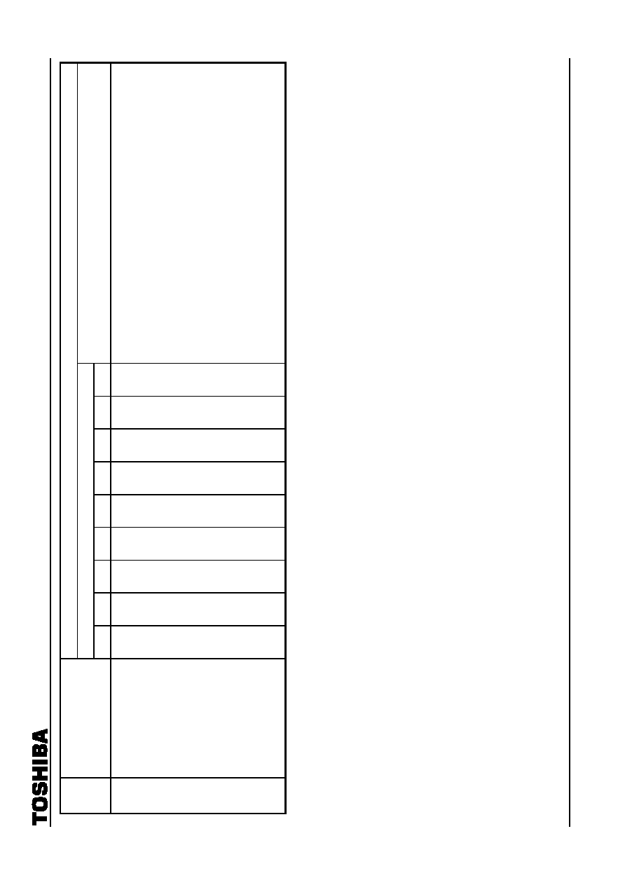
TA1276AFG
2002-04-01
62
Test Conditions (unless otherwise stated, V
CC1
=
5 V, V
CC2
/V
CC3
/DEF V
CC
=
9 V, Ta
=
25
±
3∞C)
Switching Mode
Note Parameter
SW
33
SW
34
SW
35
SW
37
SW
38
SW
39
SW
51
SW
52
SW
53
Test Conditions
A
3
Color Difference Half Tone
Characteristics
A A A A A A
A
or
B
A
or
B
C
1) Set the subaddress (10) data to (20).
2) Input signal 3 (f
0
=
100 kHz, picture period amplitude
=
0.2 V
p-p
) to pin 1.
3) Measure the picture period amplitude of the waveform output from pin 11.
(vHTA
RY
)
4) Apply 1.5 V from an external power supply to pin 6.
5) Measure the picture period amplitude of the waveform output from pin 11.
(vHTB
RY
)
6) GHT
RY
=
vHTB
RY
/vHTA
RY
7) Repeat steps 1) to 5) above with pin 13.
GHT
GY
=
vHTB
GY
/vHTA
GY
8) Repeat steps 1) to 5) above, inputting signal to pin 80 and measuring pin
15.
GHT
BY
=
vHTB
BY
/vHTA
BY
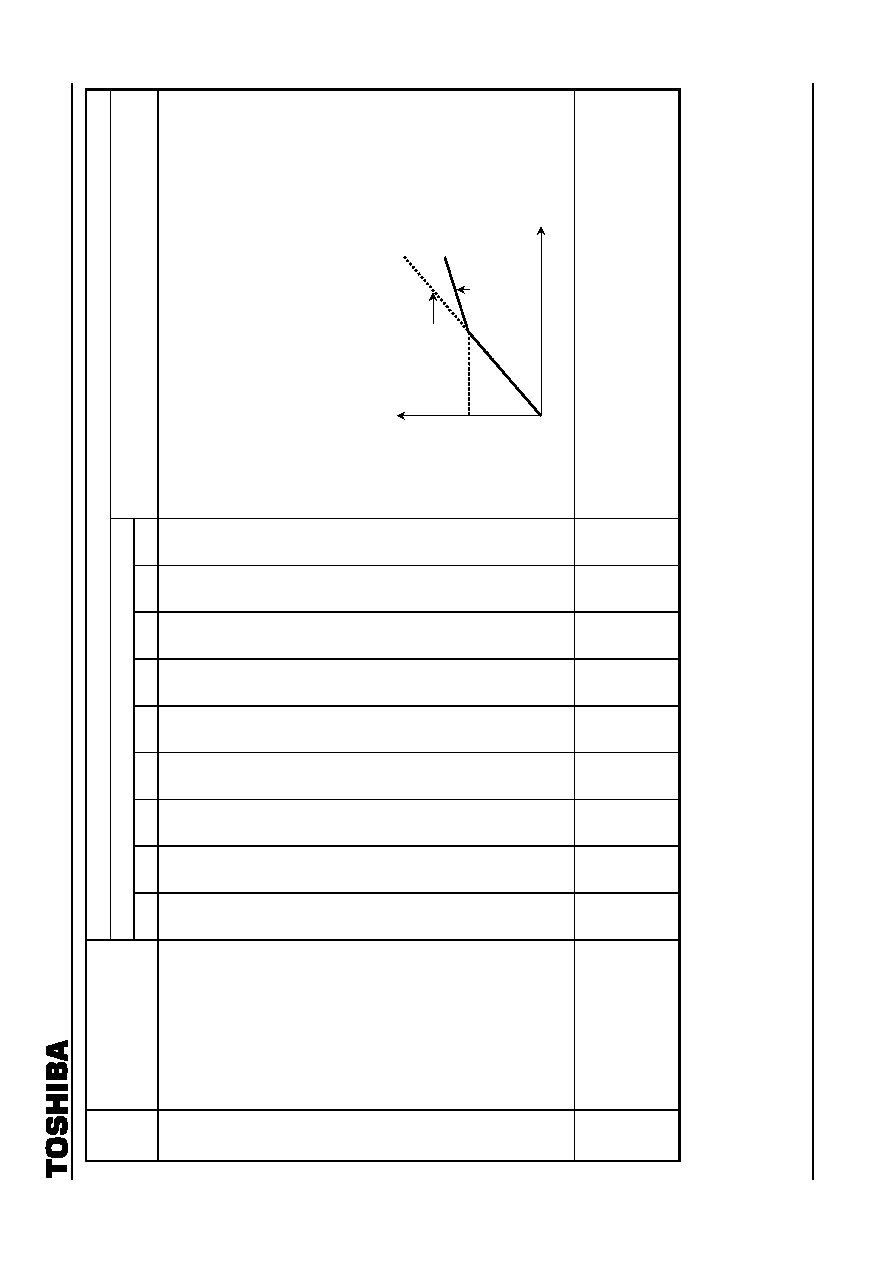
TA1276AFG
2002-04-01
63
Test Conditions (unless otherwise stated, V
CC1
=
5 V, V
CC2
/V
CC3
/DEF V
CC
=
9 V, Ta
=
25
±
3∞C)
Switching Mode
Note Parameter
SW
33
SW
34
SW
35
SW
37
SW
38
SW
39
SW
51
SW
52
SW
53
Test Conditions
A
4
Color
Characteristics
A A A A A A B B C
1) Set the subaddress (10) data to (20).
2) Input signal 2 to pin 1.
3) When the subaddress (07) data are:
(80)
-
OFF
(82)
-
1ON
(84)
-
2ON
(86)
-
3ON
measure the changes in the amplitude level of the pin 43 output signal at
an increase the amplitude A of signal 2 and plot the characteristics.
4) Calculate
the
ON gradient
, using V
, which represents the point at
which the
characteristics become effective, and the gradient of the linear
section with
OFF as (1).
A
5
Color Limiter Characteristics
A
1) Measure the voltage of pin 1.
2) Set the subaddress (10) data to (20).
3) Input signal 2 (picture period amplitude
=
0.4 V
p-p
) to pin 80.
4) Measure the picture period amplitude of the pin 11 output signal when the
subaddress (07) data are (80) and (81). (CLT0, CLT1)
OFF
V
Pin 1 input
ON
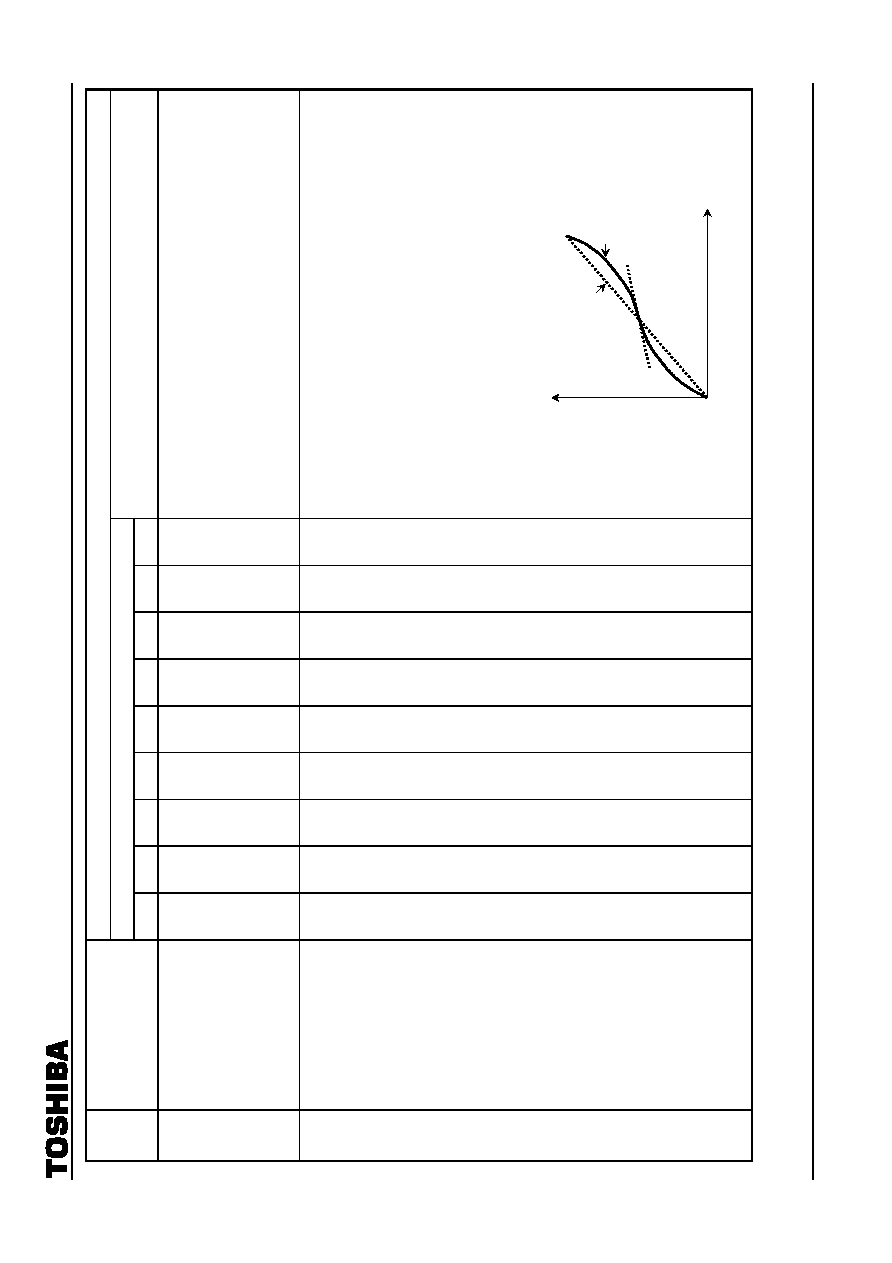
TA1276AFG
2002-04-01
64
Test Conditions (unless otherwise stated, V
CC1
=
5 V, V
CC2
/V
CC3
/DEF V
CC
=
9 V, Ta
=
25
±
3∞C)
Switching Mode
Note Parameter
SW
33
SW
34
SW
35
SW
37
SW
38
SW
39
SW
51
SW
52
SW
53
Test Conditions
A
6
High-Brightness
Color
Gain A A A A A A B A C
1) Set subaddress (10) data to (20).
2) Input signal 2 (picture period amplitude
=
0.2 V
p-p
) to pin 80.
3) Adjust the color control so that the picture period amplitude output from pin
15 is 1.2 V
p-p
.
4) Measure the picture period amplitude of the pin 15 output signal when the
subaddress (06) data are (FF). (V
41
)
5) HBC1
=
(1.2
-
V
41
)/1.2
A
7
Flesh
Color
Characteristics
A
1) Input IQ demodulated flesh-bar signals (15∞-step rainbow signals in the
range
-
30∞ to
+
240∞) to pin 80 (Q signal) and pin 1 (I signal) as 0.2 V
p-p
.
Set the brightness to maximum.
2) Set subaddress (10) data to (00).
3) Measure the signals output from pins 11 and 15 and switch to subaddress
(10) data to (06). Measure the output signals and calculate the variation
characteristics of the color vector phase.
4) Draw the vector variation characteristics curve showing the on state from
the off state and calculate the gradient in the vicinity of the I axis as Fa33.
Subaddress (08)
Data (80) off
Data (81) on
OFF
Chroma input phase [∞]
ON
Color vector phase [∞]
Fa
TA1276AFG
2002-04-01
65
Test Conditions (unless otherwise stated, V
CC1
=
5 V, V
CC2
/V
CC3
/DEF V
CC
=
9 V, Ta
=
25
±
3∞C)
Switching Mode
Note Parameter
SW
33
SW
34
SW
35
SW
37
SW
38
SW
39
SW
51
SW
52
SW
53
Test Conditions
A
8
Color
Detail
Emphasis
A A A A A A A B A
1) Connect SG to Y-IN and input a 4 MHz frequency sine wave at 20 mV
p-p
.
2) Set the subaddress (02) data to (01).
3) Set the subaddress (10) data to (20).
4) Set the subaddress (11) data to (02).
5) Read the 4 MHz amplitude output to pin 11.
(V
CDE0
)
6) Input signal 2 (picture period amplitude
=
0.3 V
p-p
) to pin 1.
7) Set the subaddress (02) data to (81).
8) Read the 4 MHz amplitude output to pin 11.
(V
CDE1
) (mV
p-p
)
9) Set the subaddress (0A) data to (81) and read the amplitude of frequency
Fp output to pin 11.
(V
CDE2
) (mV
p-p
)
10) GCD0
=
20
◊
og (
V
CDE1
-
V
CDE0
/20)
GCD1
=
20
◊
og (
V
CDE2
-
V
CDE0
/20)
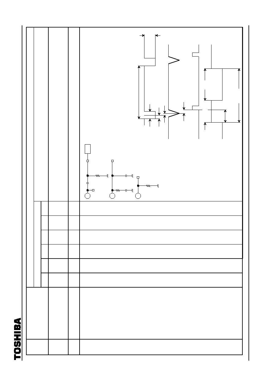
TA1276AFG
2002-04-01
66
Test Conditions (unless otherwise stated, V
CC1
=
5 V, V
CC2
/V
CC3
/DEF V
CC
=
9 V, Ta
=
25
±
3∞C)
Switching Mode
Note Parameter
SW
16
SW
17
SW
18
SW
20
SW
23
SW
25
Test Conditions
DEF
Block
DEF Block common test conditions
SW
13
: A, SW
33
: A, SW
34
: A, SW
35
: A, SW
37
: A, SW
38
: A,
SW
39
: A, SW
48
: ON, SW
49
: ON, SW
51
: B, SW
52
: B,
SW
56
: ON, BUS Data
=
power on reset
D
1
Horizontal Oscillation Control
Sensitivity
D B ON
OFF A ON
Calculate the pin 41 (H.out) frequency variation rate when the voltage on pin 45 is varied by
±
0.05 V with
a horizontal oscillation frequency of 15.734 kHz.
D
2
Horizontal Sync Phase
C
ON
Measure the phase difference S
PH1
of the pin 41 (H.out)
waveform in relation to the pin 49 (HD.out) waveform
when a 50 Hz composite video signal is applied to TP52.
Measure the phase difference S
PH2
of the pin 45
waveform in relation to the center of the input signal's
horizontal sync signal Also, apply a 60 Hz composite
video signal to pin 52 and measure S
PH3
.
0.8
µ
s
S
PH2
, S
PH3
4.7
µ
s
a
a/2
63.5
µ
s
0.25 V
Pin 41 Signal
S
PH1
41%
59%
63.5
µ
s
Pin 49 Waveform
Pin 45 Waveform
Pin 52 Input Signal
52
TG7
(sync input)
TP52
Pin 52
M
45
(AFC1 filter pin)
Pin 45
38
(H.BLK input)
Pin 38
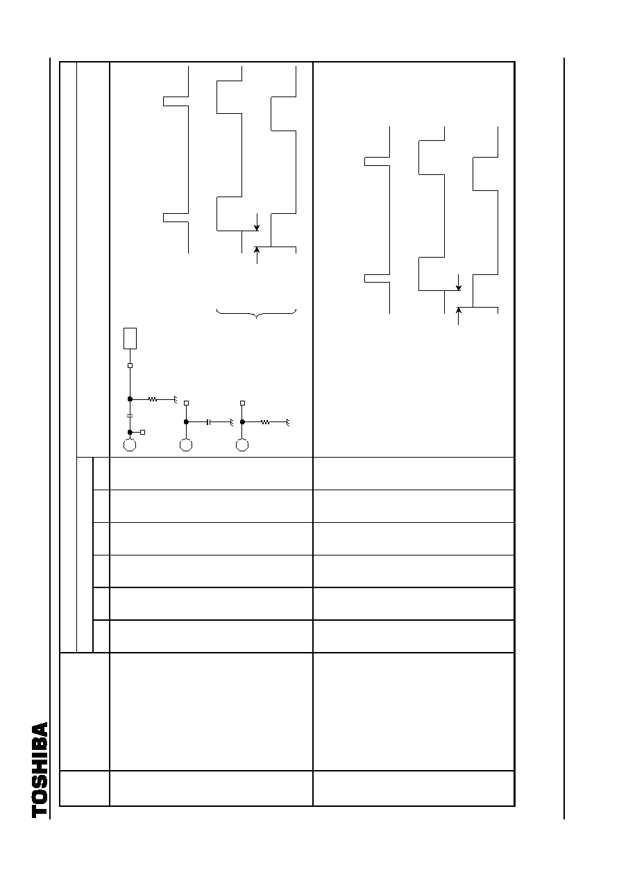
TA1276AFG
2002-04-01
67
Test Conditions (unless otherwise stated, V
CC1
=
5 V, V
CC2
/V
CC3
/DEF V
CC
=
9 V, Ta
=
25
±
3∞C)
Switching Mode
Note Parameter
SW
16
SW
17
SW
18
SW
20
SW
23
SW
25
Test Conditions
D
3
Range of Curve Correction
D
C
ON
ON
A
ON
Vary the voltage by 1.5 V to 3.5 V, apply a 50 Hz
composite video signal to pin TP52, and measure the
phase variation of the pin 41 (H.out) waveform.
D
4
Horizontal Screen Phase
Adjustment Range
Under the same conditions as those for D
3
, measure phase variation of the pin 41 (H.out) waveform
when subaddress (0B) data D
7
to D
3
are varied by (00000) to (11111).
52
TG7
(sync input)
TP52
Pin 52
M
41
(H.OUT)
Pin 41
40
(curve correction pin)
Pin 40
Pin 41
Input
Signal
H
24
Pin 40
=
3.5 V
Pin 40
=
1.5 V
Pin 49 Waveform
Pin 41
Input Signal
H
SFT
When (00000)
When (11111)
Pin 49 Waveform
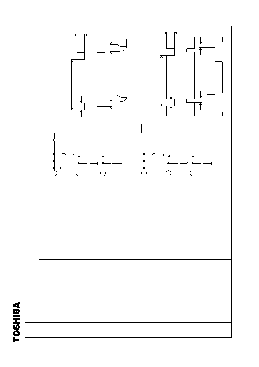
TA1276AFG
2002-04-01
68
Test Conditions (unless otherwise stated, V
CC1
=
5 V, V
CC2
/V
CC3
/DEF V
CC
=
9 V, Ta
=
25
±
3∞C)
Switching Mode
Note Parameter
SW
16
SW
17
SW
18
SW
20
SW
23
SW
25
SW
35
Test Conditions
D
5
Clamp Pulse Start Phase
Pulse Width of Clamp Pulse
D C ON
ON A ON
OPEN
Apply a 50 Hz composite video signal to TP52, then
measure the phase difference CP
S
and the pulse width
CP
W
of the pin 22 (R in) waveform in relation to the pin
49 (HD.out) waveform.
D
6
Gate Pulse Start Phase
Pulse Width of Gate Pulse
Apply a 50 Hz composite video signal to TP52, then
measure the phase difference CP
S
and the pulse width
CP
W
of the pin 70 (SCP) waveform in relation to the pin
49 (HD.out) waveform.
52
TG7
(sync input)
TP52
Pin 52
M
49
(HD.OUT)
Pin 49
22
(rin)
Pin 22
5 V
63.5
µ
s
Pin 52
Input Signal
Pin 49
Waveform
Pin 22
Waveform
CP
S
4.7
µ
s
0.25 V
CP
W
5.0 V
3.5 V
52
TG7
([illegible] input)
TP52
Pin 52
M
49
(HD.OUT)
Pin 49
70
(SCP)
Pin 70
63.5
µ
s
Pin 52
Input Signal
Pin 49
Waveform
Pin 70 Output
Waveform
CP
S
4.7
µ
s
0.25 V
CP
W
8.3 V
0 V
4.5 V
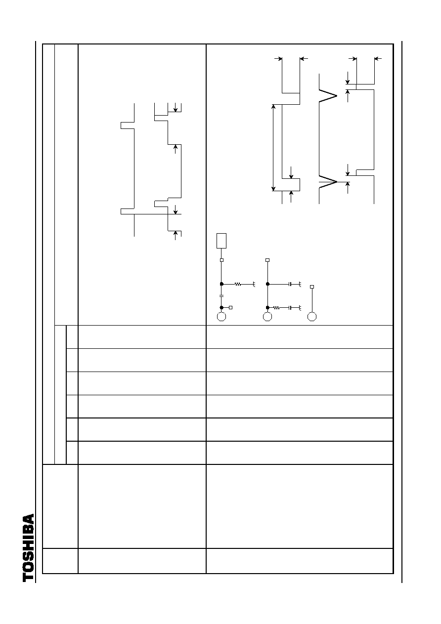
TA1276AFG
2002-04-01
69
Test Conditions (unless otherwise stated, V
CC1
=
5 V, V
CC2
/V
CC3
/DEF V
CC
=
9 V, Ta
=
25
±
3∞C)
Switching Mode
Note Parameter
SW
16
SW
17
SW
18
SW
20
SW
23
SW
25
Test Conditions
D
7
Horizontal Blanking Pulse
Start Phase
Pulse Width of Horizontal
Blanking Pulse
D C ON
ON A ON
Under the same conditions as those for D
6
, measure the phase difference HP
S
and HP
W50
of the
horizontal blanking pulse.
Also measure HP
W60
at 60 Hz.
D
8
HD Output Start Phase
HD Output Pulse Width
HD Output Amplitude
Apply a 50 Hz composite video signal to TP52, then
measure the phase difference HP
S
and the pulse width
HP
W
/V
HD
of the pin 49 (HD out) waveform in relation to
the pin 45 (AFC1 filter) waveform.
Pin 49
Waveform
Pin 70
Output Waveform
HP
S
HP
W
8.3 V
0 V
4.5 V
52
TG7
([illegible] input)
TP52
Pin 52
M
45
(AFC1 filter)
Pin 45
49
(HD output)
Pin 49
63.5
µ
s
Pin 52 Input
Waveform
Pin 45
Waveform
Pin 49 Output
Waveform
HP
S
4.7
µ
s
0.25 V
HP
W
V
HD
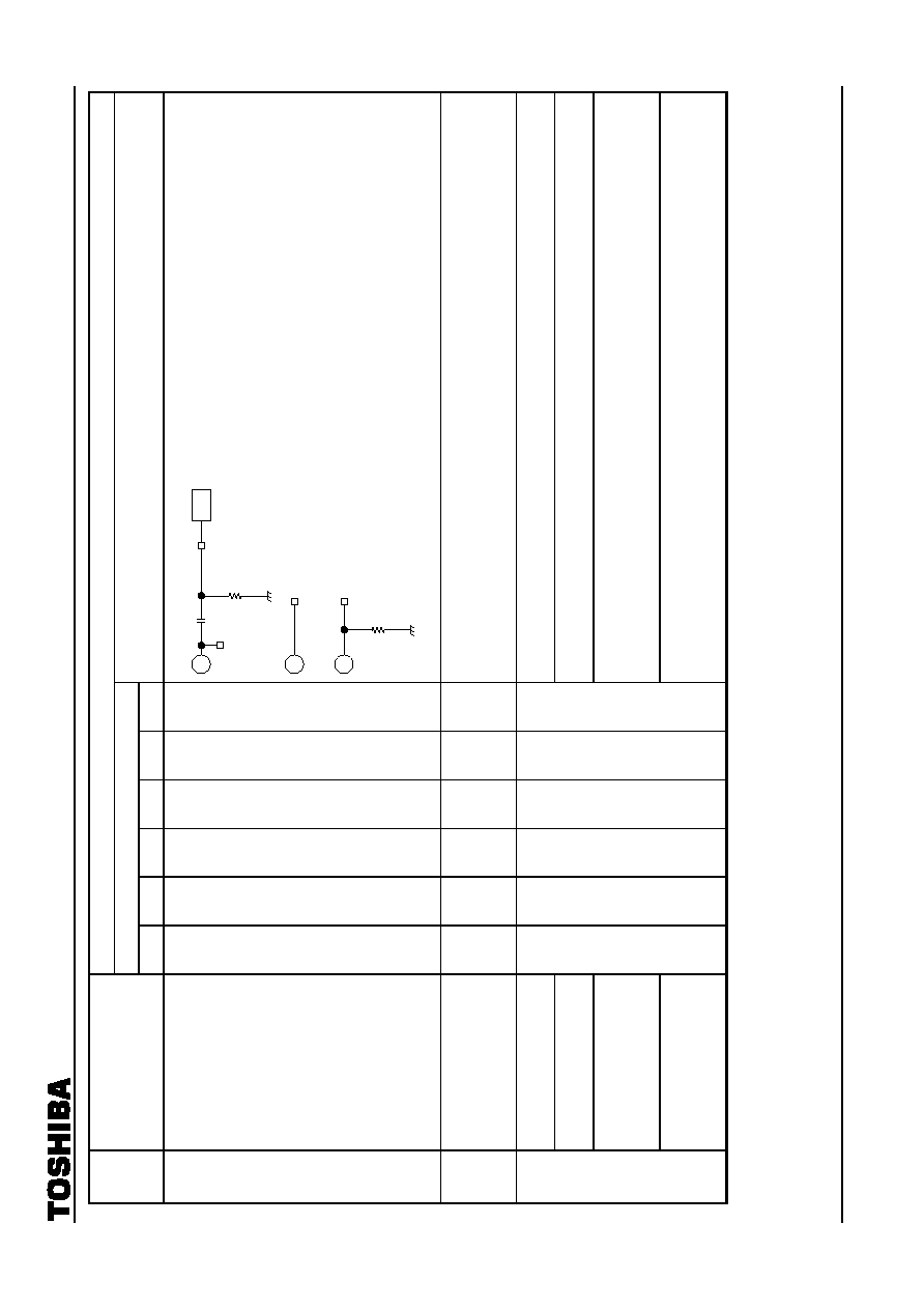
TA1276AFG
2002-04-01
70
Test Conditions (unless otherwise stated, V
CC1
=
5 V, V
CC2
/V
CC3
/DEF V
CC
=
9 V, Ta
=
25
±
3∞C)
Switching Mode
Note Parameter
SW
16
SW
17
SW
18
SW
20
SW
23
SW
25
Test Conditions
D
9
Vertical Blanking Pulse Start
Phase (1)
Vertical Blanking Pulse End
Phase (1)
D C ON
ON A ON
Apply a 50 Hz composite video signal to TP52, then
measure the phase difference VP
50S1
and the pulse
width VP
50S2
of the pin 70 (SCP) waveform in relation to
the pin 49 (sync input) waveform.
D
10
Vertical Blanking Pulse Start
Phase (2)
Vertical Blanking Pulse End
Phase (2)
Apply the same conditions as those for D
9
except change the input signal to a 60 Hz comp. video signal
and measure the phase difference VP
60S
and pulse width VP
60W
.
Vertical Pull-In Range (1)
Input a 50 Hz composite video signal to pin TP52, vary the vertical frequency of this signal in 0.5H-steps,
and measure the vertical pull-in range.
Vertical Pull-In Range (2)
Set D
5
to D
3
of subaddress (17) to (001), vary the vertical frequency of a 60 Hz composite video signal
input to pin TP52 in 0.5H-steps, and measure the vertical pull-in range.
Vertical Pull-In Range (3)
Input a 50 Hz composite video signal to pin TP52, vary the vertical frequency of this signal in 0.5H-steps,
and measure the number of Hs when D
2
of the 1
st
byte changes from 0 to 1 in bus read mode. Also check
that D
1
of the 1
st
byte is 0 when 1 V
=
312.5H, when D
1
is 1 in bus read mode, and 1 V
<
311.5 or 1 V
>
313.5H.
D
11
Vertical Pull-In Range (4)
Input a 60 Hz composite video signal to pin TP52, vary the vertical frequency of this signal in 0.5H-steps,
and measure the number of Hs when D
2
of the 1
st
byte changes from 1 to 0 in bus read mode when. Also
check that D
1
of the 1
st
byte is 0 when 1 V
=
262.5H, D
1
is 1 in bus read mode, and 1 V
<
261.5 or 1 V
>
263.5H.
52
TG7
(sync input)
TP52
Pin 52
M
47
(sync input)
Pin 47
70
(SCP)
Pin 70
TA1276AFG
2002-04-01
71
Test Conditions (unless otherwise stated, V
CC1
=
5 V, V
CC2
/V
CC3
/DEF V
CC
=
9 V, Ta
=
25
±
3∞C)
Switching Mode
Note Parameter
SW
16
SW
17
SW
18
SW
20
SW
23
SW
25
SW
33
SW
34
SW
35
SW
37
SW
38
SW
39
#
6
#
21
#
27
Test Conditions
D
12
RGB Output
Vertical Blanking Pulse Start
Phase (1)
RGB Output
Vertical Blanking Pulse End
Phase (1)
D C ON
ON A ON A
Gro-
und
Apply a 50 Hz composite video signal to TP52,
then measure the phase difference VR
50S1
and
the pulse width VR
50S2
of the pin 11 (R.out)
waveform in relation to the pin 52 (sync input)
waveform.
Similarly, measure pins 13 and 15.
D
13
RGB Output
Vertical Blanking Pulse Start
Phase (2)
RGB Output
Vertical Blanking Pulse End
Phase (2)
Apply the same conditions as those for D
12
except change the input signal to a 60 Hz
comp. video signal and measure the phase difference VP
60S1
and pulse width VP
60S2
.
52
TG7
(sync input)
TP52
Pin 52
M
11
(R output)
Pin 11
TA1276AFG
2002-04-01
72
Chroma Test Signals
Text/Color Difference Test Signals
1)
Input Signal C-1
1) Video
Signal
2)
Input Signal C-2
2)
Input Signal 1
3)
Input Signal C-3
3)
Input Signal 2
4)
Input Signal C-4
4)
Input Signal 3
Frequency f
0
sine wave
VO
Amplitude A
Y signal
1 V
p-p
C signal
Burst signal
180∞ 150∞ 120∞ 90∞ 60∞ 30∞ 0∞
-
30∞
-
60∞
-
90∞
B
u
rs
t s
i
gnal
63.5
µ
s
Frequency f
0
sine
wave
Amplitude A
Frequency f
0
sine
wave
TA1276AFG
2002-04-01
73
Vertical Output Pulse Width/Vertical Output Pulse Phase Variation/Vertical Output Pulse Phase Range
0H 1H 2H 3H 4H 5H 6H 7H 8H 9H 10H 11H 12H 13H 14H 15H 16H
T
W
T
D
Pin 29 Waveform
1H 2H 3H 4H 5H 6H 7H 8H 9H 10H 11H 12H 13H 14H 15H 16H
2
nd
Field
50 Hz Video Signal
1
st
Field
4H 5H 6H 7H 8H 9H 10H 11H 12H 13H 14H 15H 16H 17H 18H 19H
2
nd
Field
60 Hz Video Signal
1
st
Field
VP
L1
T
W
Pin 29 Waveform
VP
UN
VP
L1
T
W
Pin 29 Waveform
VP
UN
VP
L1
T
W
Pin 29 Waveform
VP
UN
VP
L1
T
W
Pin 29 Waveform
VP
UN
VP
L1
T
W
Pin 29 Waveform
VP
UN
VP
L1
T
W
Pin 29 Waveform
VP
UN
VP
L1
T
W
Pin 29 Waveform
VP
UN
VP
L1
TA1276AFG
2002-04-01
74
RGB Vertical Blanking Pulse Start Phase/End Phase
1
st
field
2
nd
field
307H 308H 309H 310H 311H 312H 313H 1H 2H 3H 4H 5H 6H 7H 8H 9H 10H 11H 12H 13H 14H 15H 16H 17H 18H 19H 20H 21H 22H 23H 24H 25H 26H
Video Signal
Pin 11/13/15
Waveform
VR 50
51
, VG 50
51
, VB 50
51
1
st
field
2
nd
field
259H 260H 261H 262H 263H 1H 2H 3H 4H 5H 6H 7H 8H 9H 10H 11H 12H 13H 14H 15H 16H 17H 18H 19H 20H 21H 22H 23H 24H 25H 26H 27H
Video Signal
Pin 11/13/15
Waveform
VR 50
51
, VG 50
51
, VB 50
51
2
nd
field
1
st
field
Video Signal
Pin 11/13/15
Waveform
2.1 V
0.8 V
VR 50
51
, VG 50
51
, VB 50
51
50 Hz
307H 308H 309H 310H 311H 312H 1H 2H 3H 4H 5H 6H 7H 8H 9H 10H 11H 12H 13H 14H 15H 16H 17H 18H 19H 20H 21H 22H 23H 24H 25H 26H
2
nd
field
1
st
field
258H 259H 260H 261H 262H 1H 2H 3H 4H 5H 6H 7H 8H 9H 10H 11H 12H 13H 14H 15H 16H 17H 18H 19H 20H 21H 22H 23H 24H 25H 26H 27H 28H
Video Signal
Pin 11/13/15
Waveform
VR 50
51
, VG 50
51
, VB 50
51
60 Hz
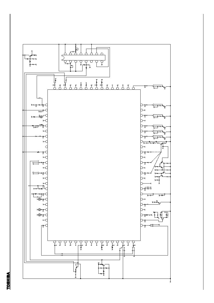
TA1276AFG
2002-04-01
75
Test Circuit
TP 41
5 k
TA1276AFG
39
0
Pin 64
Pin 62 Pin 61
12
pF
12
pF
Pin 59
12
pF
Pin 58
30
k
0.
22
µ
F
22
00
pF
10
0
µ
F
0.
01
µ
F
Pin 54
SW 54
A B
0.
01
µ
F
TP 54
Pin 52
SW 52
A C
0.
1
µ
F
TP 52
Pin 50
2.
2
µ
F
Pin 45
6.
2
k
SW 45
1 k
TP 45
0.
012
µ
F
1
µ
F
Pin 47
10
k
SW 47
Pin 41
91
SW 41
Pin 42
0.
01
µ
F
Pin 43
36
0
TP 43
49
64
63
61
60
58
56
54
53
51
50
48
46
45
44
43
42
DEF V
CC
(9
V
)
32
f
H
VCO
NC
AFC Fi
l
t
e
r
DEF GND
NC
HD
Ou
t
V.
Se
p
.
NC
Ch
r
o
m
a
GND
Ch
r
o
m
a
I
n
NC
APC Fi
l
t
e
r
NC
M
PAL X
'
t
a
l
1H
D
L
C
o
nt
V/
I
Ou
t
41
H
o
r
i
z
ont
a
l
O
u
t
p
ut
(
SW
)
62
4.
43 M
H
z
X'
t
a
l
59
3.
58 M
H
z
X'
t
a
l
57
V
CC1
(5
V
)
55
NC
52
Y
1
Sync
I
n
47
Sync
Ou
t
Pin 65
Pin 67
Pin 69
Pin 72
Pin 73
10 k
2.2
µF
2.2
µF
Pin 70
Pin 74
Pin 76
Pin 78
Pin 80
65
66
67
68
69
70
71
73
74
75
77
78
79
80 U/Q In
NC
Y
2
In
NC
NC
R S/H
Sence In
NC
SCP Out
SECAM Conto
NC
Y
1
Out
NC
U/Q Out
72 f
sc
Out
76 Color Limiter
Pin 32
Pin 29
Pin 31
Pin 27
Pin 40
Pin 38
100
100
10
µF
2.2
µF
2.2
µF
5.1 k
40
39
38
36
35
34
31
30
28
27
26
25
Analog B In
NC
Ys2 (analog RGB)
NC
NC
G S/H
SCL
SDA
NC
FBP In (BLK in)
NC
Curve odj.
(ext CP in)
29
VP Out
32
B S/H
33
NC
37
Digital GND
2 k
1
µF
0.
033
µ
F
0.
1
µ
F
Pin 2
Pin 1
20 k
30 pF
Pin 3
100 k
2 k
1
µF
Pin 5
Pin 6
SW 5
SW 3
SW 1
A
B
C
10
µ
F
TP5
0.
01
µ
F
10
0
µ
F
Pin 8
10
0 k
0.
01
µ
F
TP8
10
0
Pin 11
10
0
TP11
Pin 13
10
0
TP13
Pin 15
10
0
TP15
0.
01
µ
F
2 k
10
0
µ
F
TP15b
TP15a
2 k
1.
2
k
2 k
2 k
33
0 p
F
2 k
51
0
51
0
Pin 18
A B
0.
1
µ
F
SW 18
2 k
TP18
Pin 19
A B
0.
1
µ
F
SW 19
2 k
Pin 20
A B
0.
1
µ
F
SW 20
2 k
Pin 22
A B
0.
1
µ
F
SW 22
2 k
Pin 23
A B
0.
1
µ
F
SW 24
2 k
Pin 21
16
1
2
3
4
6
8
10
12
14
15
17
18
19
20
22
24
An
a
l
og G
I
n
An
a
l
og R
I
n
An
a
l
og O
S
D
B
I
n
An
a
l
og OSD
G I
n
An
a
l
og
O
S
D R
I
n
V
CC
2
(9
V
)
NC
B Out
NC
NC
TEXT GND
1
ABCL
I
n
YM
I
n
NC
APL De
t
.
B
l
a
ck P
e
a
k
H
o
l
d
V
/
I In
5
VSM
Out
7
V
CC
3
(9
V
)
9
TEXT GND
2
11
R Ou
t
13
G Ou
t
21
Ys
1
(
a
n
a
l
og O
S
D
)
23
NC
TP19
TP20 TP22 TP24
SW6 SW5
5.
1
k
75
10
µF
2 k
3.
9
k
TP78
V
CC
= 5 V
B
A
B
A
Pin 25
A B
0.
1
µ
F
SW 24
2 k
TP24
V
CC
= 9 V
51
k
51
k
TC45
38P
10
µF
NC
NC
5 k
12
00 pF
10
00 pF
60 k
7.5 k
1
16
2
15
3
14
4
13
5
12
6
11
7
10
8
9
3.
9
k
75
10
µF
2 k
5.
1
k
TP53b
2N
7.5 k
Pin 63
A B
TP73b
1.2 k
B
A
B
A
C
0.033
µF
0.1
µF
0.1
µF
0.1
µF
B
20 k
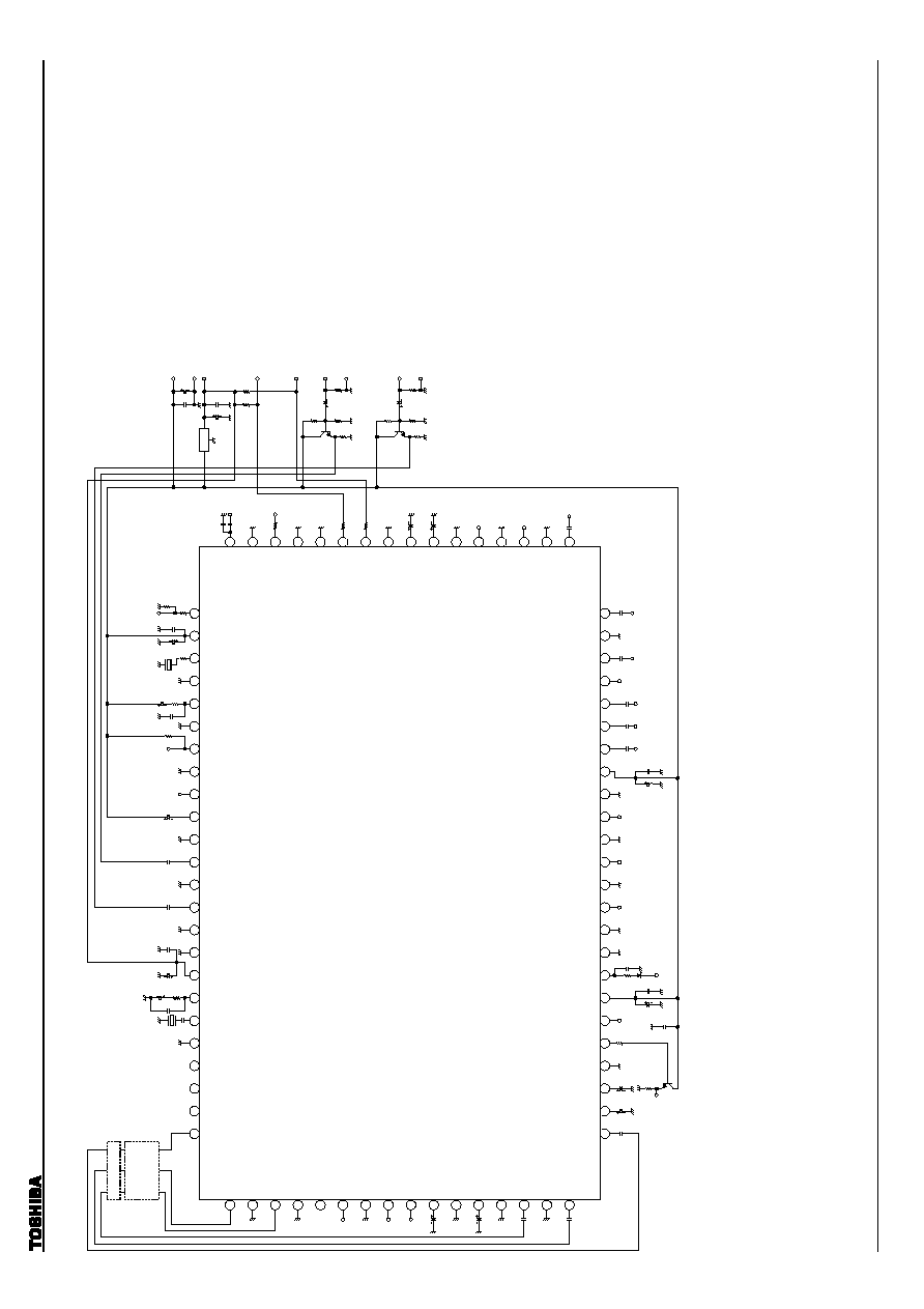
TA1276AFG
2002-04-01
76
Application Circuit 1-Normal Scan
(3.58 NTSC)
2.
2
µ
F
M
M
0.1
µF
M
G In
0.
1
µ
F
0.
1
µ
F
OSD-
G In
G Out
B Out
R Out
62
0
TA1276AFG
39
0
12
pF
30
k
0.
22
µ
F
22
00 pF
10
0
µ
F
0.
01
µ
F
2.
2
µ
F
10
k
HD Out
0.
01
µ
F
49
64
63
61
60
58
56
54
53
51
50
48
46
45
44
43
42
DEF V
CC
(9
V
)
32
f
H
VCO
NC
AFC Fi
l
t
e
r
DEF GND
NC
HD
Ou
t
V.
Se
p
.
NC
Ch
r
o
m
a
GND
Ch
r
o
m
a
I
n
NC
APC
Fi
l
t
e
r
NC
M
PAL X
'
t
a
l
1H
D
L
C
o
nt
V/
I
Ou
t
41
H
o
r
i
z
ont
a
l
O
u
t
p
ut
(
SW
)
62
4.
43 M
H
z
X'
t
a
l
59
3.
58 M
H
z
X'
t
a
l
57
V
CC1
(5
V
)
55
NC
52
Y
1
Sync
I
n
47
Sync
Ou
t
SCP
f
sc
IK In
2.2
µF
2.2
µF
65
66
67
68
69
70
71
73
74
75
77
78
79
80 U/Q In
NC
Y2 In
NC
NC
R S/H
Sence In
NC
SCP Out
SECAM Conto
NC
Y
1
Out
NC
U/Q Out
72 f
sc
Out
76 Color Limiter
VP
Ys2
0.01
µF
100
100
2.2
µF
2.2
µF
40
39
38
36
35
34
31
30
28
27
26
25
Analog B In
NC
Ys2 (analog RGB)
NC
NC
G S/H
SCL
SDA
NC
FBP In (BLK in)
NC
Curve odj.
(ext CP in)
29
VP Out
32
B S/H
33
NC
37
Digital GND
YM
0.
01
µ
F
ABL
0.
1
µ
F
OSD-
R In
16
1
2
3
4
6
8
10
12
14
15
17
18
19
20
22
24
An
a
l
og G
I
n
An
a
l
og R
I
n
An
a
l
og O
S
D
B
I
n
An
a
l
og OSD
G I
n
An
a
l
og
O
S
D R
I
n
V
CC
2
(9
V
)
NC
B Ou
t
NC
NC
TEXT GND
1
ABCL
I
n
YM
I
n
NC
APL De
t
.
Bl
a
c
k
Pea
k
H
o
l
d
V
/
I In
5
VSM
Out
7
V
CC
3
(9
V
)
9
TEXT GND
2
11
R Ou
t
13
G Ou
t
21
Ys
1
(
a
n
a
l
og O
S
D
)
23
NC
Curve
FBP
B In
0.1
µF
0.
01
µ
F
0.
1
µ
F
39
0
10
0
µ
F
1
µ
F
0.
1
µ
F
4.
7
µ
F
10
0
10
0
µ
F
0.
01
µ
F
0.
01
µ
F
10
0
µ
F
0.
1
µ
F
OSD-
B In
Ys1
R In
0.
1
µ
F
CTl
WAC
(wide aspect
converter)
0.1
µF
1 k
VSM Out
0.
01
µ
F
M
Sync Out
0.
022
µ
F
M
3.
3
k
Horizontal Output
M : mylar capacitor
10
k
10
k
75
10
µF
2.
2
k
Y In
0.
1
µ
F
47
µ
F
V
CC
5 V
5.
1
k
5.
1
k
SCL
SDA
0.
01
µ
F
47
µ
F
10
k
10
k
75
10
µF
2.
2
k
C In
Reg.
V
CC
9 V
GND
GND
GND
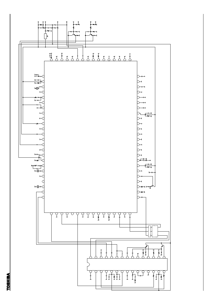
TA1276AFG
2002-04-01
77
Application Circuit 2-Normal Scan
(4.43 PAL/4.43 NTSC/3.58 NTSC)
12
pF
4.43 MHz
X'tal
TA877
2AN
0.1
µF
1 k
11 k
0.1
µF
0.01
µF
47
µF
B-Y OUT
R-Y OUT
R-Y IN
SCP
B-Y IN
0.1
µF
0.1
µF
0.1
µF
0.1
µF
10
µF 1 k
0.
1
µ
F
0.01
µF
47
µF
0.47
µF
0.47
µF
1
µF
1
µF
1
µF
1 k
0.47
µF
0.1
µF
0.1
µF
1 k
0.47
µF
1 k
1
30
2
29
3
28
4
27
5
26
6
25
7
24
8
23
9
22
10
21
11
20
12
19
13
18
14
17
15
16
WAC
(wide aspect
converter)
CTI
2.
2
µ
F
M
M
0.1
µF
M
G In
0.
1
µ
F
0.
1
µ
F
OSD-
G In
G Out
B Out
R Out
62
0
TA1276AFG
39
0
12
pF
30
k
0.
22
µ
F
22
00 pF
10
0
µ
F
0.
01
µ
F
2.
2
µ
F
10
k
HD Out
0.
01
µ
F
49
64
63
61
60
58
56
54
53
51
50
48
46
45
44
43
42
DEF V
CC
(9
V
)
32
f
H
VCO
NC
AFC Fi
l
t
e
r
DEF GND
NC
HD
Ou
t
V.
Se
p
.
NC
Ch
r
o
m
a
GND
Ch
r
o
m
a
I
n
NC
APC Fi
l
t
e
r
NC
M
PAL X
'
t
a
l
1H
D
L
C
o
nt
V/
I
Ou
t
41
H
o
r
i
z
ont
a
l
O
u
t
p
ut
(
SW
)
62
4.
43 M
H
z
X'
t
a
l
59
3.
58 M
H
z
X'
t
a
l
57
V
CC1
(5
V
)
55
NC
52
Y
1
Sync
I
n
47
Sync
Ou
t
f
sc
IK In
2.2
µF
2.2
µF
65
66
67
68
69
70
71
73
74
75
77
78
79
80 U/Q In
NC
Y2 In
NC
NC
R S/H
Sence In
NC
SCP Out
SECAM Conto
NC
Y
1
Out
NC
U/Q Out
72 f
sc
Out
76 Color Limiter
VP
Ys2
0.01
µF
100
100
2.2
µF
2.2
µF
40
39
38
36
35
34
31
30
28
27
26
25
Analog B In
NC
Ys2 (analog RGB)
NC
NC
G S/H
SCL
SDA
NC
FBP In (BLK in)
NC
Curve odj.
(ext CP in)
29
VP Out
32
B S/H
33
NC
37
Digital GND
YM
0.
01
µ
F
ABL
0.
1
µ
F
OSD-
R In
16
1
2
3
4
6
8
10
12
14
15
17
18
19
20
22
24
An
a
l
og G
I
n
An
a
l
og R
I
n
An
a
l
og O
S
D
B
I
n
An
a
l
og OSD
G I
n
An
a
l
og
O
S
D R
I
n
V
CC
2
(9
V
)
NC
B Ou
t
NC
NC
TEXT GND
1
ABCL
I
n
YM
I
n
NC
APL De
t
.
B
l
a
ck P
e
a
k
H
o
l
d
V/
I
I
n
5
VSM
Out
7
V
CC
3
(9
V
)
9
TEXT GND
2
11
R Ou
t
13
G Ou
t
21
Ys
1
(
a
n
a
l
og O
S
D
)
23
NC
Curve
FBP
B In
0.1
µF
0.
01
µ
F
0.
1
µ
F
39
0
10
0
µ
F
1
µ
F
0.
1
µ
F
2.
2
µ
F
10
0
10
0
µ
F
0.
01
µ
F
0.
01
µ
F
10
0
µ
F
0.
1
µ
F
OSD-
B In
Ys1
R In
0.
1
µ
F
0.1
µF
1 k
VSM Out
0.
01
µ
F
M
Sync Out
0.
022
µ
F
M
3.
3
k
Horizontal Output
M : mylar capacitor
10
k
10
k
75
10
µF
2.
2
k
Y In
0.
1
µ
F
47
µ
F
V
CC
5 V
5.
1
k
5.
1
k
SCL
SDA
0.
01
µ
F
47
µ
F
10
k
10
k
75
10
µF
2.
2
k
C In
Reg.
V
CC
9 V
3.58 MHz
X'tal
GND
GND
GND
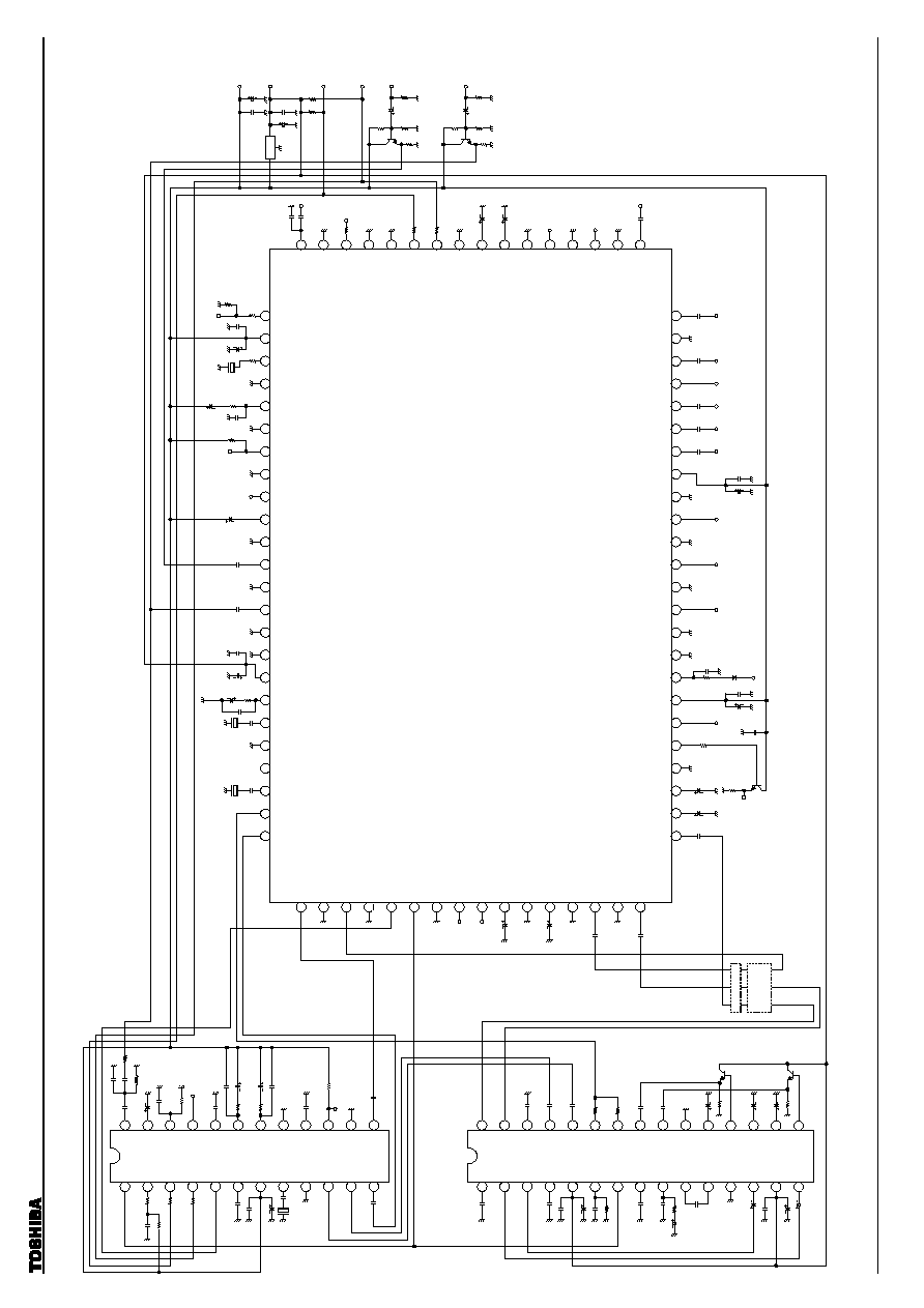
TA1276AFG
2002-04-01
78
Application Circuit 3-Normal Scan
(4.43 PAL/4.43 NTSC/3.58 NTSC/SECAM)
V
CC
5 V
V
CC
9 V
TA1276AFG
62
0
4.43 MHz
X'tal
12
pF
30
k
0.
22
µ
F
22
00 pF
10
0
µ
F
0.
01
µ
F
Sync Out
M
2.
2
µ
F
10
k
2.2
µF
VP
Ys2
100
100
Cuver
2.2
µF
2.2
µF
1 k
YM
0.
01
µ
F
10
0
µ
F
0.
01
µ
F
10
0
0.
1
µ
F
0.
1
µ
F
0.
1
µ
F
VSM
Out
TA122
9N
SCL
C IN
1 k
Bell
HD Out
ABL
0.1
µF
0.01
µF
FBP
0.1
µF
10
k
10
k
75
10
µF
2.
2
k
Y In
0.
1
µ
F
47
µ
F
5.
1
k
5.
1
k
SCL
SDA
0.
01
µ
F
47
µ
F
10
k
10
k
75
10
µF
2.
2
k
C In
Reg.
0.
1
µ
F
1
µ
F
2.
2
µ
F
0.
01
µ
F
10
0
µ
F
0.
01
µ
F
0.
1
µ
F
0.
1
µ
F
3.58 MHz
X'tal
12
pF
0.
022
µ
F
0.
01
µ
F
0.
1
µ
F
3.
3
k
2.
2
µ
F
M
39
0
10
0
µ
F
0.
01
µ
F
39
0
Horizontal
Output
2.2
µF
0.1
µF
M
M
0.1
µF
M
0.1
µF
M
82 pF
1000 pF
1000 pF
4.7 M
27
µH
0.02
µF
M
10
µF
0.056
µF
1 k
0.68 pF
M
91 pF
510
0.022 pF
M
10 k
DAC
10 k
100
100
92 pF
24 k
91 pF
15 pF
0.01
µF
47
µF
4 MHz
X'tal
(NR18)
B-Y OUT
R-Y OUT
R-Y IN
SDA
SCP
Bell
Moni
TA877
2AN
0.1
µF
1 k
11 k
0.1
µF
0.01
µF
47
µF
B-Y OUT
R-Y OUT
R-Y IN
SCP
B-Y IN
0.1
µF
0.1
µF
0.1
µF
0.1
µF
10
µF 1 k
0.
1
µ
F
0.01
µF
47
µF
0.47
µF
0.47
µF
1
µF
1
µF
1
µF
1 k
0.47
µF
0.1
µF
0.1
µF
1 k
0.47
µF
1 k
49
64
63
61
60
58
56
54
53
51
50
48
46
45
44
43
42
DEF V
CC
(9
V
)
32
f
H
VCO
NC
AFC Fi
l
t
e
r
DEF GND
NC
HD
Ou
t
V.
Se
p
.
NC
Ch
r
o
m
a
GND
Ch
r
o
m
a
I
n
NC
APC Fi
l
t
e
r
NC
M
PAL X
'
t
a
l
1H
D
L
C
o
nt
V/
I
Ou
t
41
H
o
r
i
z
ont
a
l
O
u
t
p
ut
(
SW
)
62
4.
43 M
H
z
X'
t
a
l
59
3.
58 M
H
z
X'
t
a
l
57
V
CC1
(5
V
)
55
NC
52
Y
1
Sync
I
n
47
Sync
Ou
t
65
66
67
68
69
70
71
73
74
75
77
78
79
80 U/Q In
NC
Y
2
In
NC
NC
R S/H
Sence In
NC
SCP Out
SECAM Conto
NC
Y
1
Out
NC
U/Q Out
72 f
sc
Out
76 Color Limiter
40
39
38
36
35
34
31
30
28
27
26
25
Analog B In
NC
Ys2 (analog RGB)
NC
NC
G S/H
SCL
SDA
NC
FBP In (BLK in)
NC
Curve odj.
(ext CP in)
29
VP Out
32
B S/H
33
NC
37
Digital GND
16
1
2
3
4
6
8
10
12
14
15
17
18
19
22
24
An
a
l
og G
I
n
An
a
l
og R
I
n
An
a
l
og OSD
B
I
n
An
a
l
o
g
OSD
G I
n
An
a
l
og
OSD R
I
n
V
CC
2
(9
V
)
NC
B Out
NC
NC
TEXT GND
1
ABCL
I
n
YM
I
n
NC
APL De
t
.
Bl
a
c
k
Pea
k
H
o
l
d
V/
I
I
n
5
7
V
CC
3
(9
V
)
9
TEXT GND
2
11
R Ou
t
13
G Ou
t
21
Ys
1
(
a
n
a
l
og O
S
D
)
23
NC
1
24
2
23
3
22
4
21
5
20
6
19
7
18
8
17
20
9
16
10
15
11
14
12
13
1
30
2
29
3
28
4
27
5
26
6
25
7
24
8
23
9
22
10
21
11
20
12
19
13
18
14
17
15
16
WAC
(wide aspect
converter)
CTI
M
B In
M : mylar capacitor
G In
R In
Ys1
B Out
G Out
R Out
OSD-
B In
OSD-
G In
OSD-
R In
VSM Out
2.2
µF
2.2
µF
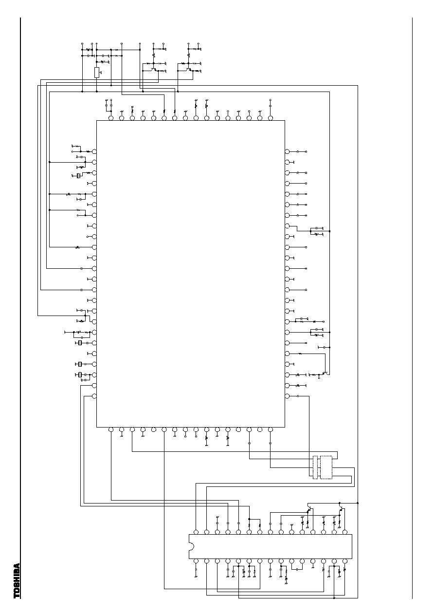
TA1276AFG
2002-04-01
79
Application Circuit 4-Normal Scan
(3.58 NTSC/M-PAL/N-PAL)
TA1276AFG
62
0
N-PAL
X'tal
12
pF
30
k
0.
22
µ
F
22
00 pF
10
0
µ
F
0.
01
µ
F
Sync Out
M
2.
2
µ
F
10
k
2.2
µF
VP
Ys2
100
100
Cuver
2.2
µF
2.2
µF
1 k
YM
0.
01
µ
F
10
0
µ
F
0.
01
µ
F
10
0
0.
1
µ
F
0.
1
µ
F
0.
1
µ
F
VSM
Out
HD Out
ABL
0.1
µF
0.01
µF
FBP
0.1
µF
10
k
10
k
75
10
µF
2.
2
k
Y In
0.
1
µ
F
47
µ
F
V
CC
5 V
5.
1
k
5.
1
k
SCL
SDA
0.
01
µ
F
47
µ
F
10
k
10
k
75
10
µF
2.
2
k
C In
Reg.
0.
1
µ
F
1
µ
F
2.
2
µ
F
0.
01
µ
F
10
0
µ
F
0.
01
µ
F
0.
1
µ
F
0.
1
µ
F
3.58 MHz
X'tal
12
pF
0.
022
µ
F
0.
01
µ
F
0.
1
µ
F
3.
3
k
2.
2
µ
F
M
39
0
10
0
µ
F
0.
01
µ
F
39
0
Horizontal
Output
2.2
µF
M
0.1
µF
M
TA877
2AN
0.1
µF
1 k
11 k
0.1
µF
0.01
µF
47
µF
B-Y OUT
R-Y OUT
R-Y IN
SCP
B-Y IN
0.1
µF
0.1
µF
0.1
µF
0.1
µF
10
µF 1 k
0.
1
µ
F
0.01
µF
47
µF
0.47
µF
0.47
µF
1
µF
1
µF
1
µF
1 k
0.47
µF
0.1
µF
0.1
µF
1 k
0.47
µF
1 k
49
64
63
61
60
58
56
54
53
51
50
48
46
45
44
43
42
DEF V
CC
(9
V
)
32
f
H
VCO
NC
AFC Fi
l
t
e
r
DEF GND
NC
HD
Ou
t
V.
Se
p
.
NC
Ch
r
o
m
a
GND
Ch
r
o
m
a
I
n
NC
APC Fi
l
t
e
r
NC
M
PAL X
'
t
a
l
1H
D
L
C
o
nt
V/
I
Ou
t
41
H
o
r
i
z
ont
a
l
O
u
t
p
ut
(
SW
)
62
4.
43 M
H
z
X'
t
a
l
59
3.
58 M
H
z
X'
t
a
l
57
V
CC1
(5
V
)
55
NC
52
Y
1
Sync
I
n
47
Sync
Ou
t
65
66
67
68
69
70
71
73
74
75
77
78
79
80 U/Q In
NC
Y
2
In
NC
NC
R S/H
Sence In
NC
SCP Out
SECAM Conto
NC
Y
1
Out
NC
U/Q Out
72 f
sc
Out
76 Color Limiter
40
39
38
36
35
34
31
30
28
27
26
25
Analog B In
NC
Ys2 (analog RGB)
NC
NC
G S/H
SCL
SDA
NC
FBP In (BLK in)
NC
Curve odj.
(ext CP in)
29
VP Out
32
B S/H
33
NC
37
Digital GND
16
1
2
3
4
6
8
10
12
14
15
17
18
19
22
24
An
a
l
og G
I
n
An
a
l
og R
I
n
An
a
l
og O
S
D
B
I
n
An
a
l
og OSD
G I
n
An
a
l
og
O
S
D R
I
n
V
CC
2
(9
V
)
NC
B Out
NC
NC
TEXT GND
1
ABCL
I
n
YM
I
n
NC
APL De
t
.
B
l
a
ck P
e
a
k
H
o
l
d
V
/
I In
5
7
V
CC
3
(9
V
)
9
TEXT GND
2
11
R Ou
t
13
G Ou
t
21
Ys
1
(
a
n
a
l
og O
S
D
)
23
NC
20
1
30
2
29
3
28
4
27
5
26
6
25
7
24
8
23
9
22
10
21
11
20
12
19
13
18
14
17
15
16
WAC
(wide aspect
converter)
CTI
M
B In
V
CC
9 V
M : mylar capacitor
G In
R In
Ys1
B Out
G Out
R Out
OSD-
B In
OSD-
G In
OSD-
R In
VSM Out
M-PAL
X'tal
12
pF
1 pF
IK In
f
sc
GND
GND
GND
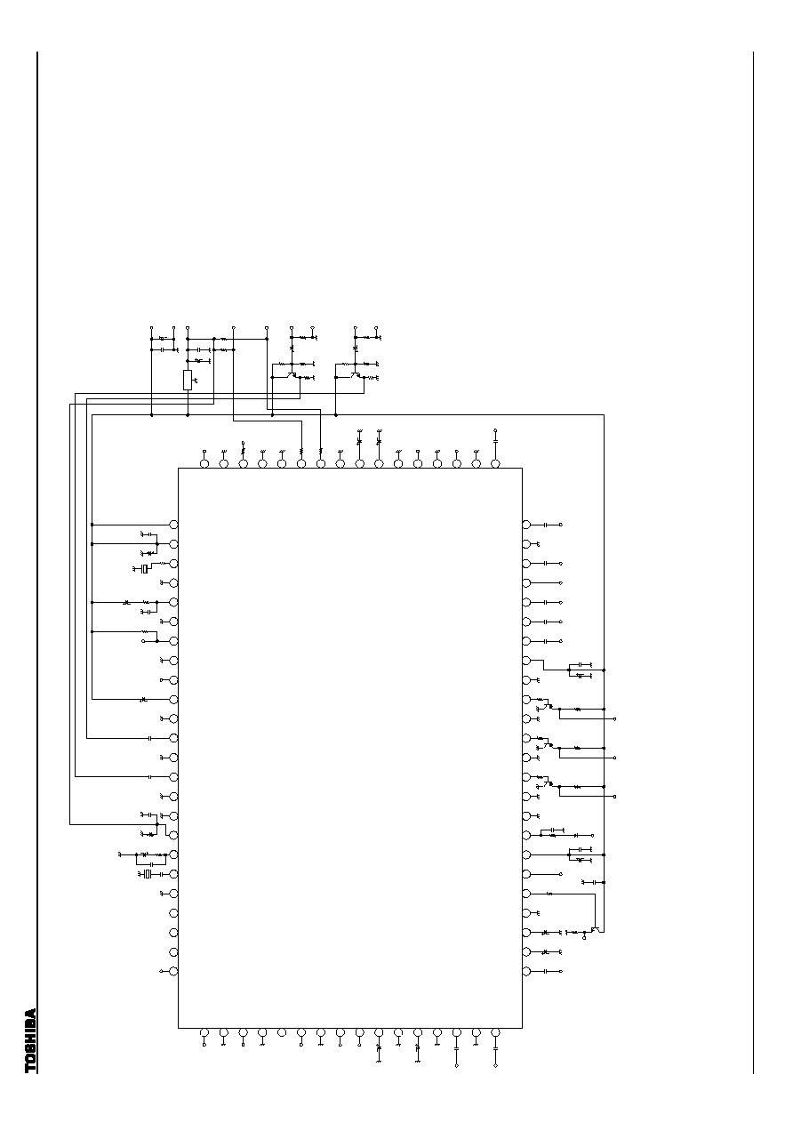
TA1276AFG
2002-04-01
80
Application Circuit 5-Double Scan
(3.58 NTSC)
TA1276AFG
30
k
0.
22
µ
F
22
00 pF
10
0
µ
F
0.
01
µ
F
Sync Out
M
2.
2
µ
F
10
k
2.2
µF
VP (1H)
Ys2
100
100
2.2
µF
2.2
µF
1 k
YM
0.
01
µ
F
10
0
µ
F
0.
01
µ
F
10
0
0.
1
µ
F
0.
1
µ
F
0.
1
µ
F
VSM
Out
HD Out
ABL
0.1
µF
0.1
µF
10
k
10
k
75
10
µF
2.
2
k
Y In
0.
1
µ
F
47
µ
F
V
CC
5 V
5.
1
k
5.
1
k
SCL
SDA
0.
01
µ
F
47
µ
F
10
k
10
k
75
10
µF
2.
2
k
C In
Reg.
0.
1
µ
F
1
µ
F
2.
2
µ
F
0.
01
µ
F
10
0
µ
F
0.
01
µ
F
0.
1
µ
F
0.
1
µ
F
V/I Out
(1H)
12
pF
0.
022
µ
F
0.
01
µ
F
0.
1
µ
F
3.
3
k
2.
2
µ
F
M
39
0
10
0
µ
F
0.
01
µ
F
2.2
µF
M
49
64
63
61
60
58
56
54
53
51
50
48
46
45
44
43
42
DEF V
CC
(9
V
)
32
f
H
VCO
NC
AFC Fi
l
t
e
r
DEF GND
NC
HD
Ou
t
V.
Se
p
.
NC
Ch
r
o
m
a
GND
Ch
r
o
m
a
I
n
NC
APC Fi
l
t
e
r
NC
M
PAL X
'
t
a
l
1H
D
L
C
o
nt
V/
I
Ou
t
41
H
o
r
i
z
ont
a
l
O
u
t
p
ut
(
SW
)
62
4.
43 M
H
z
X'
t
a
l
59
3.
58 M
H
z
X'
t
a
l
57
V
CC1
(5
V
)
55
NC
52
Y
1
Sync
I
n
47
Sync
Ou
t
65
66
67
68
69
70
71
73
74
75
77
78
79
80 U/Q In
NC
Y
2
In
NC
NC
R S/H
Sence In
NC
SCP Out
SECAM Conto
NC
Y
1
Out
NC
U/Q Out
72 f
sc
Out
76 Color Limiter
40
39
38
36
35
34
31
30
28
27
26
25
Analog B In
NC
Ys2 (analog RGB)
NC
NC
G S/H
SCL
SDA
NC
FBP In (BLK in)
NC
Curve odj.
(ext CP in)
29
VP Out
32
B S/H
33
NC
37
Digital GND
16
1
2
3
4
6
8
10
12
14
15
17
18
19
22
24
An
a
l
og G
I
n
An
a
l
og R
I
n
An
a
l
og O
S
D
B
I
n
An
a
l
og OSD
G I
n
An
a
l
og
O
S
D R
I
n
V
CC
2
(9
V
)
NC
B Out
NC
NC
TEXT GND
1
ABCL
I
n
YM
I
n
NC
APL De
t
.
Bl
a
c
k
Pea
k
H
o
l
d
V
/
I In
5
7
V
CC
3
(9
V
)
9
TEXT GND
2
11
R Ou
t
13
G Ou
t
21
Ys
1
(
a
n
a
l
og O
S
D
)
23
NC
20
M
B In
V
CC
9 V
M : mylar capacitor
G In
R In
Ys1
B Out
G Out
R Out
OSD-
B In
OSD-
G In
OSD-
R In
VSM Out
U/Q Out
(1H)
Y
1
Out
(1H)
SCP
f
sc
IK In
U/Q In
(2H)
0.1
µF
M
Y
2
In
(2H)
Ext
CP/BPP
(2H)
Ext
H/V BLK
(2H)
GND
GND
GND
V/I In
(2H)
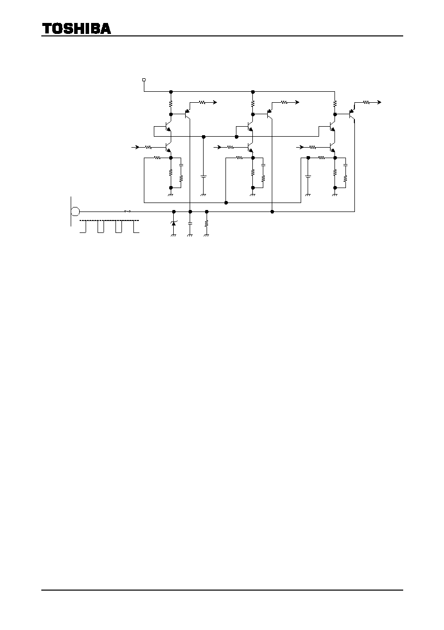
TA1276AFG
2002-04-01
81
AKB Application Circuit
20 t
o
51
k
51 pF t
o
330 pF
CRT CRT
R
G
CRT
73
B
+B
3.
3 V
Z
Sence In
R
G
B
1 to 2 V

TA1276AFG
2002-04-01
82
Package Dimensions
Weight: 1.6 g (typ.)

TA1276AFG
2002-04-01
83
∑ TOSHIBA is continually working to improve the quality and reliability of its products. Nevertheless, semiconductor
devices in general can malfunction or fail due to their inherent electrical sensitivity and vulnerability to physical
stress. It is the responsibility of the buyer, when utilizing TOSHIBA products, to comply with the standards of
safety in making a safe design for the entire system, and to avoid situations in which a malfunction or failure of
such TOSHIBA products could cause loss of human life, bodily injury or damage to property.
In developing your designs, please ensure that TOSHIBA products are used within specified operating ranges as
set forth in the most recent TOSHIBA products specifications. Also, please keep in mind the precautions and
conditions set forth in the "Handling Guide for Semiconductor Devices," or "TOSHIBA Semiconductor Reliability
Handbook" etc..
∑ The TOSHIBA products listed in this document are intended for usage in general electronics applications
(computer, personal equipment, office equipment, measuring equipment, industrial robotics, domestic appliances,
etc.). These TOSHIBA products are neither intended nor warranted for usage in equipment that requires
extraordinarily high quality and/or reliability or a malfunction or failure of which may cause loss of human life or
bodily injury ("Unintended Usage"). Unintended Usage include atomic energy control instruments, airplane or
spaceship instruments, transportation instruments, traffic signal instruments, combustion control instruments,
medical instruments, all types of safety devices, etc.. Unintended Usage of TOSHIBA products listed in this
document shall be made at the customer's own risk.
∑ The products described in this document are subject to the foreign exchange and foreign trade laws.
∑ The information contained herein is presented only as a guide for the applications of our products. No
responsibility is assumed by TOSHIBA CORPORATION for any infringements of intellectual property or other
rights of the third parties which may result from its use. No license is granted by implication or otherwise under
any intellectual property or other rights of TOSHIBA CORPORATION or others.
∑ The information contained herein is subject to change without notice.
000707EBA
RESTRICTIONS ON PRODUCT USE