 | –≠–ª–µ–∫—Ç—Ä–æ–Ω–Ω—ã–π –∫–æ–º–ø–æ–Ω–µ–Ω—Ç: TA1316AN | –°–∫–∞—á–∞—Ç—å:  PDF PDF  ZIP ZIP |

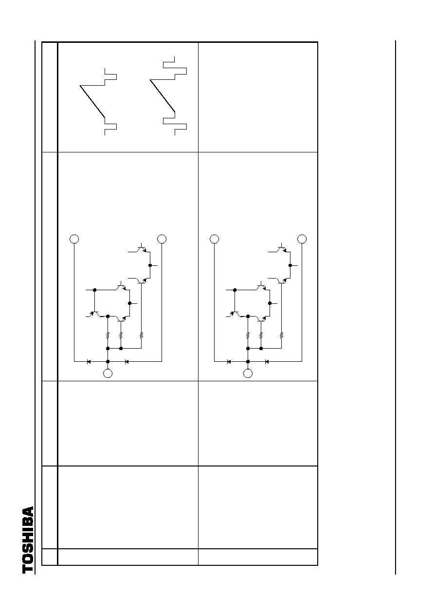
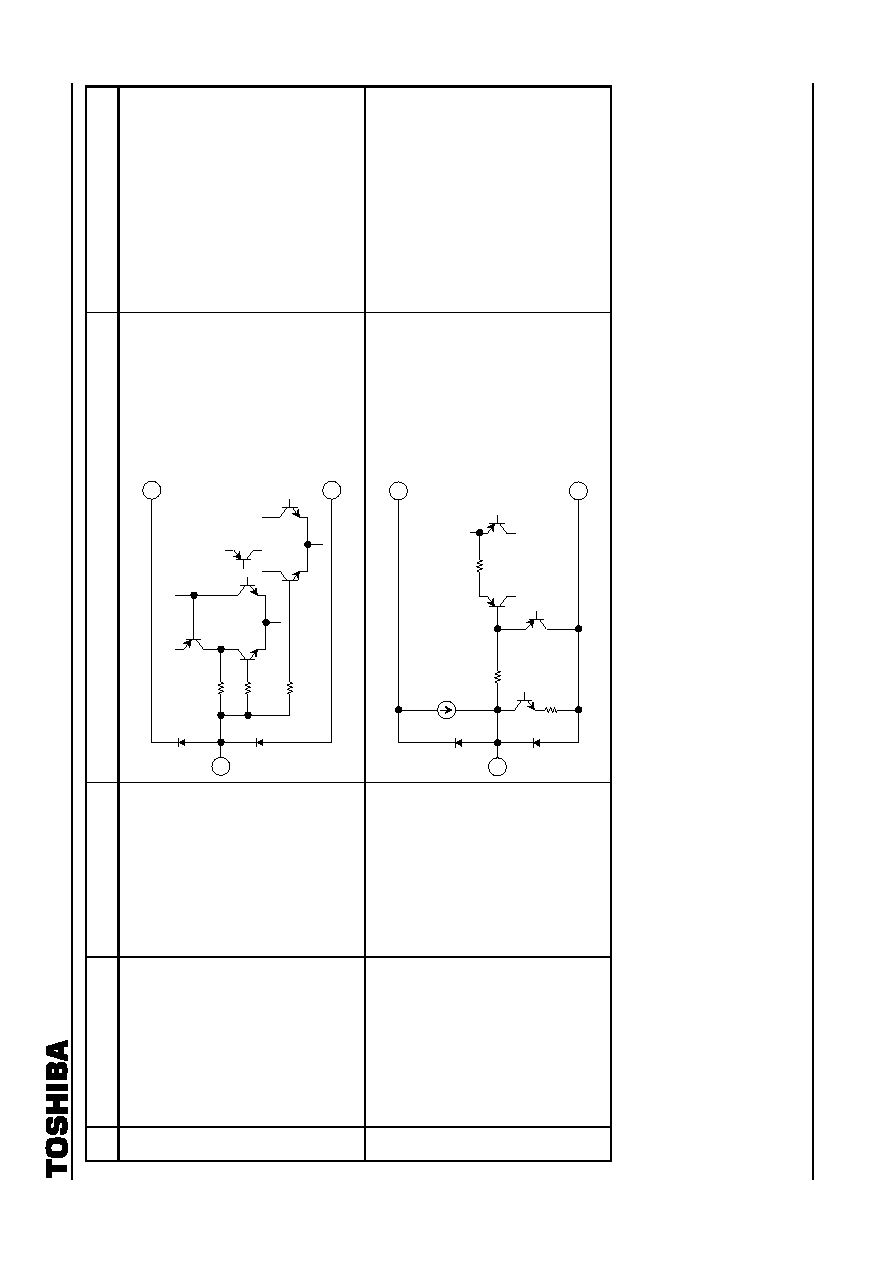
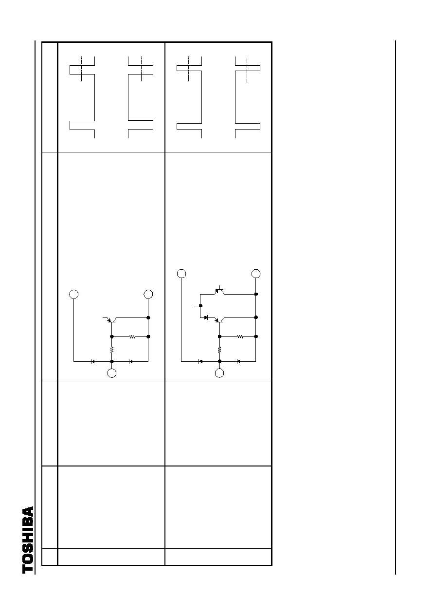
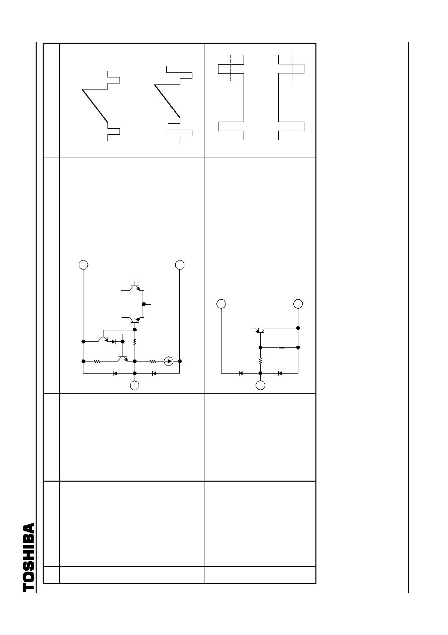
TA1316AN
2002-10-04
1
Toshiba Bipolar Linear Integrated Circuit Silicon Monolithic
TA1316AN
YCbCr/YPbPr Signal and Sync Processor for Digital TV, Progressive Scan TV and Double
Scan TV
TA1316AN is a component signal and sync processor for Digital
TV, Progressive scan TV and Double scan TV.
TA1316AN provides high performance signal processors in the
luminance and color difference blocks. The sync circuit can
process 525I/P, 625I/P, 750P, 1125I/P, PAL100 Hz and
NTSC120 Hz formats.
TA1316AN provides I
2
C bus interface, so various functions and
controls are adjustable via the bus.
Features
Luminance Block
∑ Black stretch, DC restoration
∑ Dynamic correction
∑ SRT (LTI)
∑ Y group delay correction (shoot balance correction)
∑ APACON white peak limit
∑ White pulse limit (white letter improvement)
∑ Hi-bright color
∑ Color detail enhancer (CDE)
∑ VSM output
Color Difference Block
∑ Flesh color correction
∑ Dynamic Y/C correction
∑ Color SRT (CTI)
∑ Color
∑ White peak blue correction
Text Block
∑ OSD blending SW
∑ ACB (only black level)
∑ 2 analog RGB inputs
Synchronization Block
∑ Horizontal synchronization
(15.75 kHz, 31.5 kHz, 33.75 kHz, 45 kHz)
∑ Vertical synchronization
(525I/P, 625I/P, 750P, 1125I/P, PAL 100 Hz, NTSC 120 Hz)
∑ 2-and 3-level sync. separation circuit
∑ Accept both positive and negative HD/VD input
∑ Mask for copy-guard signal
∑ Vertical blanking
Weight: 5.55 g (typ.)
TA1316AN
2002-10-04
2
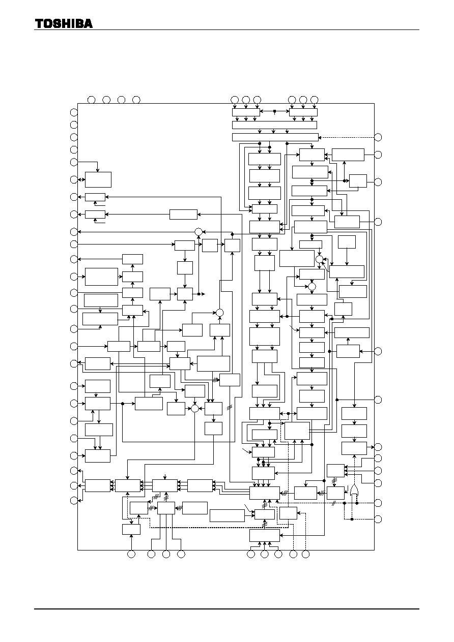
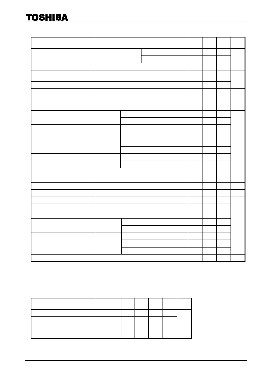
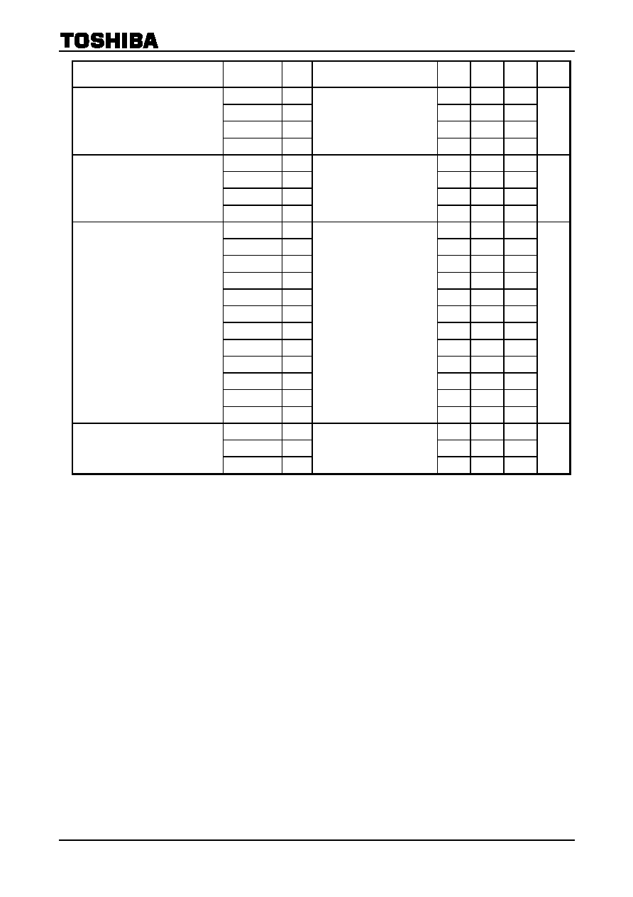
Block Diagram
DAC2
(ACB PLUSE)
HORIZONTAL
FREQUENCY
SW
AFC FILTER
H CURVE
CORRECTION
DE
F
/
D
A
C V
CC
SW
HORIZONTAL
PHASE
I
2
CBUS
DECODER
H
FREQUENCY
SW
CLAMP
H DUTY
I
2
L V
DD
I
2
L GND
Y1
IN
C
b1
/P
b1
IN
C
r1
/P
r1
IN
DE
F
/
D
A
C GND
VP OUT
Y
HD
PbPr/YCbCr YUV CONVERT
SW
H CURVE
CORRECTION
SYNC
SEPA
HD IN SW
V
INTEGRAL
VD IN SW
RGB OUT
H C/D
HVCO
H-AFC
H-RAMP
2
◊
f
H
V C/D
V
FREQUENCY
SW
ACB
PULSE
HD
POLARITY
CLAMP
PULSE
EXT
V-BLK
H-BLK
V-BLK
V-CLP
DRIVE
CLAMP
BLK
SW
I
K
CUT OFF
RGB
BRIGHTNESS
CLAMP
RGB
CONTRAST
MIXER SW/
BLUE BACK
RGB
MATRIX
CLAMP
WP BLUE
HALF TONE
/C MUTE
COLOR
G-Y
MATRIX
RELATIVE
PHASE/
AMPLITUDE
H-BPP
V-BPP
UNI-COLOR
COLOR
CLAMP
PULSE
CP
SW
EXT
CP
CP/BPP
SYNC OUT
BPP
SW
EXT
BPP
DL/
COLOR
SRT
TINT
Y/C LEVEL
COMP
SW
IQ UV
CONVERTER
UV IQ
CONVERTER
FRESH
COLOR
CLAMP
Y2
IN
C
b2
/P
b2
IN
C
r2
/P
r2
IN
BLACK
STRETCH
BLACK PEAK
DETECT
DARK
DET
BLACK LEVEL
CORECTION
DYNAMIC
DC REST
SHARPNESS
DELAY LINE
APL
DETECT
GROUP
DELAY
CORRECTION
YNR
SRT
WPL
CLAMP
UNI-
COLOR
APACON
WPL
SUB-
CONTRAST
WPS
HALF TONE
HI-BRIGHT
COLOR
Yout-
COLOR
PEAK
DETECT
SHARPNESS
CONTROL
Y DETAIL
CONTROL
CDE
BRIGHTNESS
ABCL
AMP
VSM
MUTE
VSM AMP
HPF
OSD
AMP
CLAMP
OSD
ACL SW
Y
M
SW
MATRIX SW
DARK AREA
DET FILTER
BPH FILTER
APL FILTER
ABCL IN
COLOR
LIMITER
ANALOG
OSD G IN
ANALOG
OSD R IN
VSM OUT
ANALOG
OSD B IN
Y
S
1
(ANALOG OSD)
Y
S
2
(ANALOG OSD)
I
K
IN
AN
AL
O
G
R I
N
R S/
H
G S
/
H
B S/H
AN
AL
O
G
GI
N
AN
AL
O
G
B IN
Y
S
3
(A
NA
LOG
RGB
)
Y
M
/P-
MU
T
E
/
B
L
K
Y/C V
CC
RGB GND
Y/C GND
RGB V
CC
SCL
SDA
SCP OUT
SCP IN
HVCO
H-OUT
FBP IN
VP OUT
SYNC IN
VD1 IN
HD1 IN
HD2 IN
VD2 IN
R OUT
G OUT
B OUT
CP
CP
CP
CP
DAC2
DAC1
CP
CP
OR
S/H
CP
SW
19
25
29
32
3
4
5
8
9
10
6
55
44
40
31
30
28
36
18
26
17
22
21
20
23
24
27
14
16
13
15
12
43
42
41
38
37
51
50
54
39
11
53
56
1
2
7
45
48
47
46
35
34
33
49 52
+
+
+
+
+
Y
B-Y
G-Y
R-Y
Y
V
U
FBP/BLK
TA1316AN
2002-10-04
3
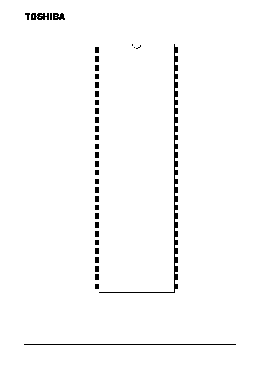
Pin Assignment
APL FILTER
56
Y/C V
CC
VSM OUT
ABCL IN
Y
M
/P-MUTE/BLK
Y
S
1 (analog OSD)
55
54
53
52
51
50
DARK AREA DET FILTER
1
2
3
4
5
6
7
BPH FILTER
Y1 IN
C
b1
/P
b1
IN
C
r1
/P
r1
IN
Y/C GND
MATRIX SW
Y
S
2 (analog OSD)
Y2 IN
8
9
10
11
12
13
14
C
b2
/P
b2
IN
C
r2
/P
r2
IN
COLOR LIMITER
VD2 IN
HD2 IN
SYNC IN
VD1 IN 15
16
17
18
19
20
21
HD1 IN
SCP IN
SCP OUT
DEF/DAC V
CC
AFC FILTER
HVCO
HORIZONTAL FREQUENCY SW 22
23
24
25
26
27
28
H CURVE CORRECTION
FBP IN
DEF/DAC GND
H-OUT
VP OUT
Y
S
3 (analog RGB)
49
R S/H
G S/H
48
47
B S/H
46
I
K
IN
RGB GND
R OUT
G OUT
B OUT
45
44
43
42
41
40 RGB V
CC
ANALOG OSD R IN
39
ANALOG OSD G IN
ANALOG OSD B IN
38
37
DAC2 (ACB pulse)
36
ANALOG R IN
ANALOG G IN
ANALOG B IN
I
2
L GND
SDA
35
34
33
32
31
30 SCL
I
2
L V
DD
29
TA1316AN
TA1316AN
2002-10-04
4
Pin Functions
Pin
No.
Pin Name
Function
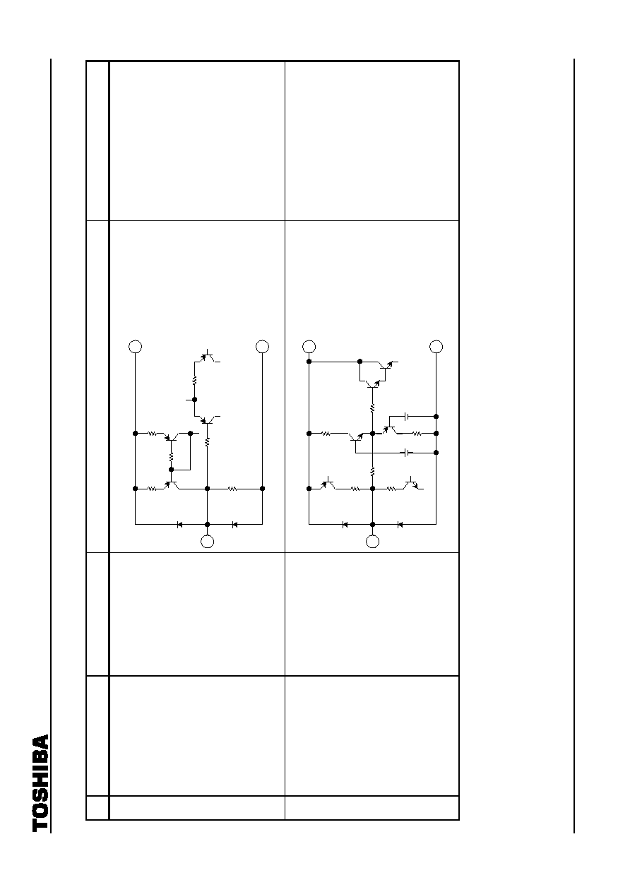
Interface Circuit
Input Signal/Output Signal
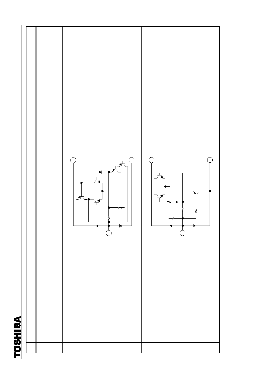
1
DARK AREA DET
FILTER
Connect filter for detecting
black area.
Voltage value of this pin
controls dynamic
circuit gain.
DC
2 BPH
FILTER
Connect filter for detecting
black peak.
Voltage value of this pin
controls black stretch gain.
DC
55
1
6
50 k
5 k
55
2
6
1 k
200
4 k
1 k
1 k
1 k
5 V
4.
25 V
TA1316AN
2002-10-04
5
Pin
No.
Pin Name
Function
Interface Circuit
Input Signal/Output Signal
3 Y1
IN
Inputs Y1 signal via clamp
capacitor.
Recommended input
amplitude: 1 V
p-p
(including
sync) at 100% color bar.
1 V
p-p
(including sync) at 100% color bar
or
4 C
b1
/P
b1
IN
Inputs C
b1
/P
b1
signal via
clamp capacitor.
Recommended input
amplitude: 700 mV
p-p
at 100%
color bar.
700 mV
p-p
at 100% color bar for C
b1
/P
b1
55
3
6
1 k
1 k
5 k
55
4
6
1 k
1 k
5 k

TA1316AN
2002-10-04
6
Pin
No.
Pin Name
Function
Interface Circuit
Input Signal/Output Signal
5 C
r1
/P
r1
IN
Inputs C
r1
/P
r1
signal via clamp
capacitor.
Recommended input
amplitude: 700 mV
p-p
at 100%
color bar.
100 mV
p-p
at 100% color bar for C
r1
/P
r1
6
Y/C GND
GND pin for Y/C block.
7 MATRIX
SW
Matrix switching pin for YCbCr
or YPbPr input.
Switches matrix according to
voltage value input to this pin
when BUS control "YUV
INPUT MODE"
=
00 or 01.
Then, control by pin has
priority over control by BUS
(see table 4).
When pin is not used, connect
0.01
µ
F capacitor between pin
and GND.
When YUV INPUT MODE
=
00 or 01,
0~0.6 V: YCbCr
Internal YUV
0.9~5 V: YPbPr
Internal YUV
Open: BUS control
55
5
6
1 k
1 k
5 k
55
7
6
1 k
112 k
25
µ
A
BUS
TA1316AN
2002-10-04
7
Pin
No.
Pin Name
Function
Interface Circuit
Input Signal/Output Signal
8 Y2
IN
Inputs Y2 signal via clamp
capacitor.
Recommended input
amplitude: 1 V
p-p
(including
sync) at 100% color bar.
1 V
p-p
(including sync) at 100% color bar
or
9 Cb2/Pb2
IN
Inputs C
b2
/P
b2
signal via
clamp capacitor.
Recommended input
amplitude: 700 mV
p-p
at 100%
color bar.
700 mV
p-p
at 100% color bar for C
b2
/P
b2
55
8
6
1 k
1 k
5 k
55
9
6
1 k
1 k
5 k
TA1316AN
2002-10-04
8
Pin
No.
Pin Name
Function
Interface Circuit
Input Signal/Output Signal
10 C
r2
/P
r2
IN
Inputs C
r2
/P
r2
signal via clamp
capacitor.
Recommended input
amplitude: 700 mV
p-p
at 100%
color bar.
700 mV
p-p
at 100% color bar for C
r2
/P
r2
11 COLOR
LIMITER
Connect filter for detecting
color limit.
DC
55
10
6
1 k
1 k
5 k
55
11
6
5 k
7
µ
A
TA1316AN
2002-10-04
9
Pin
No.
Pin Name
Function
Interface Circuit
Input Signal/Output Signal
12 VD2
IN
Inputs vertical sync signal
VD2. Signal input can have
both positive and negative
polarity.
or
13 HD2
IN
Inputs horizontal sync signal
HD2. Signal input can have
both positive and negative
polarity.
or
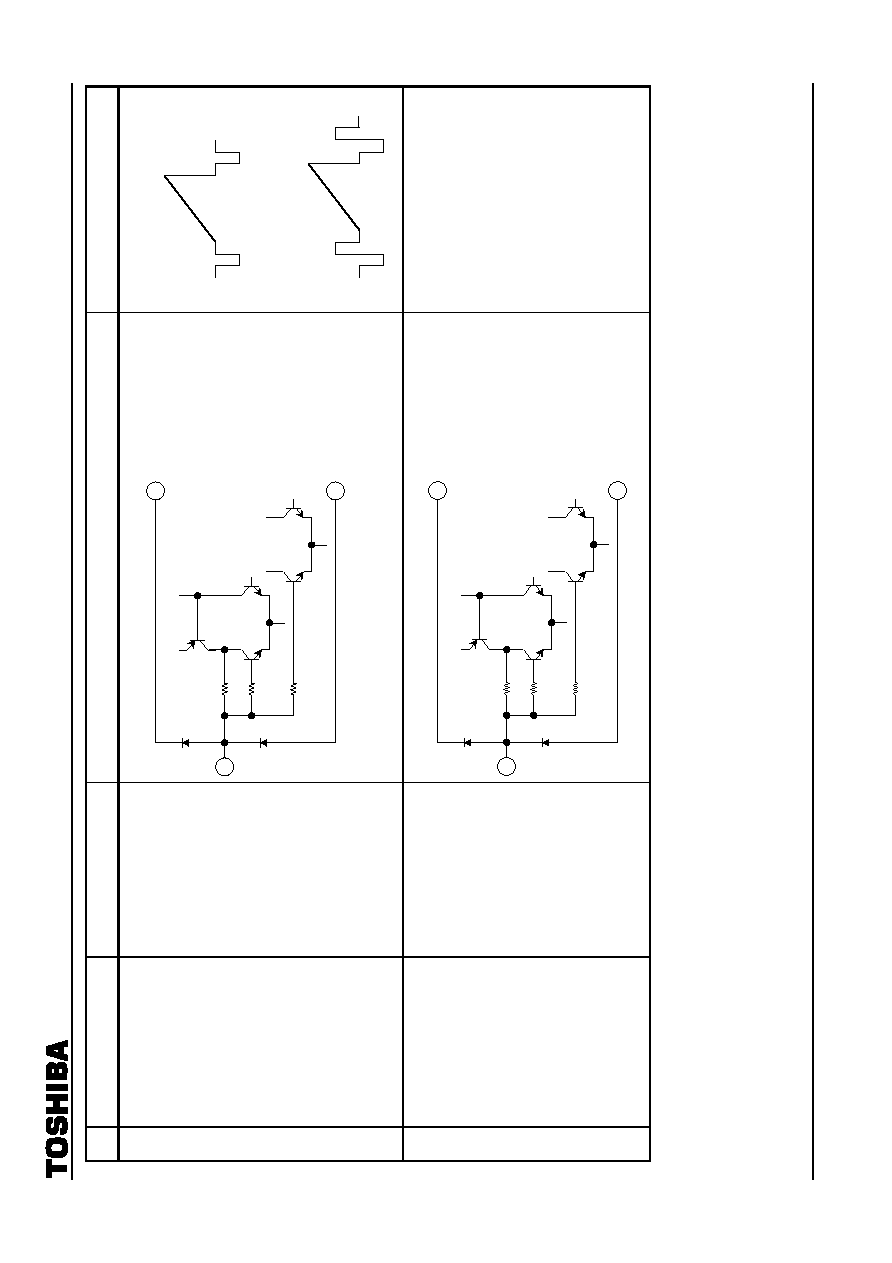
19
12
25
1 k
45 k
19
13
25
1 k
50 k
Threshold:
0.75 V
Threshold:
0.75 V
Threshold:
0.75 V
Threshold:
0.75 V
TA1316AN
2002-10-04
10
Pin
No.
Pin Name
Function
Interface Circuit
Input Signal/Output Signal
14 SYNC
IN
Inputs sync signal via clamp
capacitor.
White 100%: 1 V
p-p
or
15 VD1
IN
Inputs vertical sync signal
VD1. Signal input can have
both positive and negative
polarity.
or
19
15
25
1 k
45 k
Threshold:
0.75 V
Threshold:
0.75 V
19
14
25
1 k
1 k
10
µ
A
1 k

TA1316AN
2002-10-04
11
Pin
No.
Pin Name
Function
Interface Circuit
Input Signal/Output Signal
16 HD1
IN
Inputs horizontal sync signal
HD1. Input signal can have
both positive and negative
polarity.
or
17 SCP
IN
Inputs SCP from up converter.
Input signals are clamp pulse
(CP) and black peak detection
stop pulse (BPP).
2.2 V~2.8 V: BPP
4.7 V~9 V: CP
18 SCP
OUT
Outputs SCP.
Output signals are clamp pulse
(CP) and black peak detection
stop pulse (BPP).
(Note) Don't use
Horizontal-BPP (H-BPP) for
the timing pulse of picture
period on the screen (e.g.
H-BLK) because H-BPP width
will be changed by the
temperature.
19
16
25
1 k
50 k
19
18
25
500
2.
5 k
200
CP: 5.0 V
BPP: 2.5 V
0 V
19
17
25
5 k
50 k
50 k
40 k
Threshold:
0.75 V
Threshold:
0.75 V
TA1316AN
2002-10-04
12
Pin
No.
Pin Name
Function
Interface Circuit
Input Signal/Output Signal
19 DEF/DAC
V
CC
V
CC
pin for DEF/DAC block.
To ascertain the correct
voltage for V
CC
, please refer to
the table entitled Maximum
Ratings.
20 AFC
FILTER
Connect filter for detecting
AFC.
DC
21 HVCO
Connect ceramic oscillator for
horizontal oscillation.
Use Murata
CSBLA503KECZF30
oscillator.
19
21
25
2 k
10 k
1 k
1 k
19
20
25
300
30 k

TA1316AN
2002-10-04
13
Pin
No.
Pin Name
Function
Interface Circuit
Input Signal/Output Signal
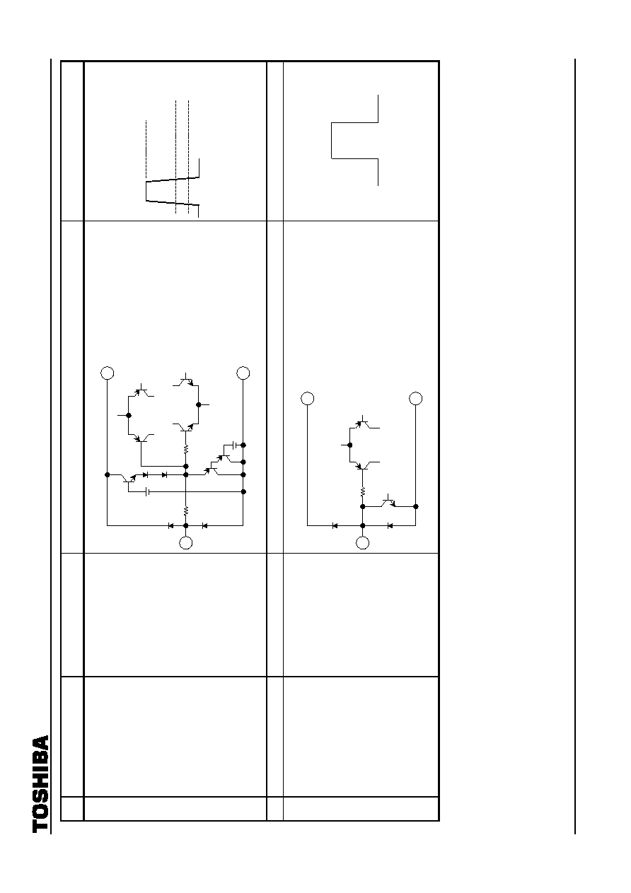
22
HORIZONTAL
FREQUENCY
SW
Horizontal frequency select
pin.
Selects horizontal frequency
according to voltage value
input to this pin.
When selecting horizontal
frequency by BUS control,
leave pin open. Control by pin
has priority over control by
BUS.
When this IC will be used on
CRT, the frequency of H-out
(pin 26) should be controlled
by DC voltage which is divided
from voltage of DEF V
CC
(pin
19) by resisters.
At BUS control (horizontal frequency):
output voltage value
00 (15.75 kHz): DC 9 V
01 (31.5 kHz): DC 6 V
10 (33.75 kHz): DC 3 V
11 (45 kHz):
DC 0 V
At pin 22 control, horizontal frequency
and input voltage value
0~1.0
V:
45
kHz
2.0~4.0
V:
33.75
kHz
5.0~7.0
V:
31.5
kHz
8.0~9.0
V:
15.75
kHz
23
H CURVE
CORRECTION
Corrects curve at high-tension
fluctuation.
Input AC component of
high-tension fluctuation.
When pin is not used, connect
0.01
µ
F capacitor between pin
and GND.
DC
23
1 k
65 k
19
25
25 k
50 k
130 k
6.5 V
19
25
22
1 k
30 k
1 k
20 pF
60 k
60 k
60 k
16 k
15
k
4.5 V
7.5 V
1.5 V
TA1316AN
2002-10-04
14
Pin
No.
Pin Name
Function
Interface Circuit
Input Signal/Output Signal
24 FBP
IN
Input FBP and H-BLK for
horizontal AFC.
25 DEF/DAC GND
GND pin for DEF/DAC block.
26 H-OUT
Horizontal output pin. Open
collector output.
max: 9 V
H-AFC threshold: 3.0 V
BLK threshold: 1.5 V
24
19
25
500
1 k
5 V
2.
25 V
19
26
25
5 k
TA1316AN
2002-10-04
15
Pin
No.
Pin Name
Function
Interface Circuit
Input Signal/Output Signal
27 VP
OUT
Outputs vertical pulse.
When a current is applied to
the pin, external blanking is
carried out by ORing this
signal with the internal
blanking signal.
(Note) When H-POSITION will
be changed, VP width will
change. Use the start phase of
VP.
V-BLK input current: 780
µ
A~1 mA
28 DAC1
(SYNC OUT)
Outputs 1-bit DAC or
composite SYNC signal after
sync separation.
Open-collector output
(The output level for this pin
cannot be guaranteed since
leakage from internal signals
may occur.)
DC or SYNC OUT
29 I
2
L V
DD
V
DD
pin for I
2
L block.
Connect 2 V (typ.).
Power to pin 29 should be
supplied from pin 19 via zener
diode through resister.
5 V
0 V
Start phase
VP output:
19
25
28
500
32
19
25
27
200
200
µ
A
32
TA1316AN
2002-10-04
16
Pin
No.
Pin Name
Function
Interface Circuit
Input Signal/Output Signal
30 SCL
SCL pin for I
2
C BUS.
31 SDA
SDA pin for I
2
C BUS.
32 I
2
L GND
GND pin for I
2
L block.
19
30
32
5 k
25
SCL
2.
25 V
19
31
32
5 k
25
SDA
2.
25 V
50
ACK
TA1316AN
2002-10-04
17
Pin
No.
Pin Name
Function
Interface Circuit
Input Signal/Output Signal
33
34
35
ANALOG B IN
ANALOG G IN
ANALOG R IN
Inputs analog R/G/B signal via
clamp capacitor.
Recommended input
amplitude: 0.7 V
p-p
(no sync)
at 100% white
100 IRE: 0.7 V
p-p
36
DAC2
(ACB pulse)
Outputs 1-bit DAC or ACB
pulse
Open-collector output
DC or ACB pulse
40
44
1 k
33
34
35
1 k
1 k
40
36
44
500
TA1316AN
2002-10-04
18
Pin
No.
Pin Name
Function
Interface Circuit
Input Signal/Output Signal
37
38
39
ANALOG OSD B IN
ANALOG OSD G IN
ANALOG OSD R IN
Inputs analog OSD signal via
clamp capacitor.
Recommended input
amplitude: 0.7 V
p-p
(no sync)
at 100% white
100 IRE: 0.7 V
p-p
40 RGB
V
CC
V
CC
pin for text/RGB block.
To ascertain the correct
voltage for V
CC
, please refer to
the table entitled Maximum
Ratings.
41
42
43
B OUT
G OUT
R OUT
Outputs R/G/B signal.
Recommended output
amplitude: 100 IRE
=
2.3 V
p-p
100 IRE: 2.3 V
p-p
Conditions:
UNI-COLOR
=
max
SUB-CONT
=
Cent
Y
IN
=
0.7 V
p-p
44 RGB GND
GND pin for text/RGB block.
40
44
1 k
37
38
39
1 k
1 k
40
44
41
42
43
200
100
2.
7 m
A
TA1316AN
2002-10-04
19
Pin
No.
Pin Name
Function
Interface Circuit
Input Signal/Output Signal
45 I
K
IN
Inputs the feedback signal
from CRT. (BLK level should
be 0 V to 3 V.)
When ACB is not used,
connect this pin to the RGB
V
CC
pin.
or RGB V
CC
46
47
48
B S/H
G S/H
R S/H
Sample-and-hold (S/H) pin.
In ACB mode connect a 2.2-
µ
F
capacitor. In CUTOFF mode
connect a 0.01-
µ
F capacitor.
DC
40
45
44
1 k
40
44
46
47
48
500
1 k
5 k
3 pF
3 V
1 V
p-p
(typ.)
R G B
0 V~3 V
TA1316AN
2002-10-04
20
Pin
No.
Pin Name
Function
Interface Circuit
Input Signal/Output Signal
49 Y
S
3
(analog RGB)
Selects input between internal
RGB and external analog RGB
according to voltage value
input to this pin.
When analog RGB is selected,
mutes VSM output.
0~0.5 V: Internal
1.5~9 V: Analog RGB, VSM mute
50
51
Y
S
2
(analog OSD)
Y
S
1
(analog OSD)
Switches between internal
RGB and OSD input signals.
Voltage applied to Y
S
1 and
Y
S
2 adjusts blend ratio of
internal RGB and OSD signals.
When Y
S
1 or Y
S
2 is High,
mutes VSM output.
Y
S
2 Y
S
1
Blend ratio
Int RGB:
OSD RGB
L L 10:0
H L 7:3
L H 5:5
H H 0:10
0~0.5 V: Internal
1.1~1.7 V: VSM mute
2.9~9 V: OSD, VSM mute
40
49
44
300
300
40
44
50
51
300
50 k

TA1316AN
2002-10-04
21
Pin
No.
Pin Name
Function
Interface Circuit
Input Signal/Output Signal
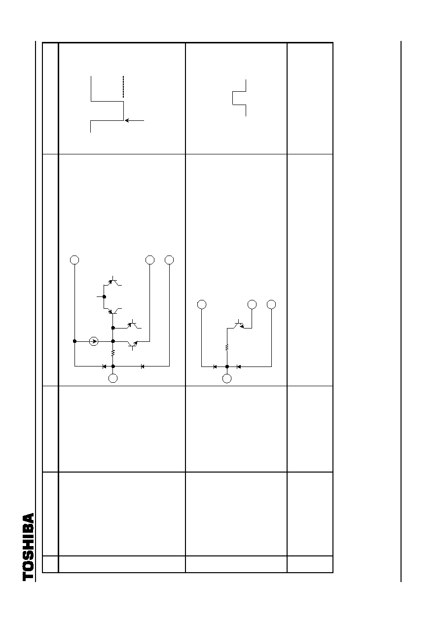
52 Y
M
/P-MUTE/BLK
Fast half-tone switch for
internal RGB signal.
Also performs image mute or
blanking.
0~0.5 V: Internal
1.2~1.8 V: Half-tone
2.7~4.0 V: P-mute
7~9 V:
Blanking
53 ABCL
IN
ABL and ACL input pin.
Can set gain and start point for
ABL and dynamic ABL by BUS
control.
DC
53
44
40
30 k
3 k
6.
75 V
40
52
44
300
80 k
10 k
TA1316AN
2002-10-04
22
Pin
No.
Pin Name
Function
Interface Circuit
Input Signal/Output Signal
54 VSM
OUT
Outputs Y signal for VSM
which passes through HPF
circuit (primary differential
circuit).
Mutes output signal using pins
49, 50 and 51.
55 Y/C
V
CC
V
CC
pin for Y/C block.
To ascertain the correct
voltage for V
CC
, please refer to
the table entitled Maximum
Ratings.
56 APL
FILTER
Connect filter for correcting DC
restoration.
Leaving this pin open enables
user to monitor Y signal after
black stretch and dynamic
.
55
56
6
1 k
40 k
1 k
40
54
6
200
200
1 k
1.
6 m
A
TA1316AN
2002-10-04
23
Bus Control Map
Write Mode
Slave Address: 88H
Sub-Add
D7 D6 D5 D4 D3 D2 D1 D0 Preset
00 H-FREQ
H-DUTY
YUV-SW
DAC1
DAC2
SYNC
INPUT-SW
1000
0000
01 HORIZONTAL
POSITION
CLP-PHS
1000
0000
02 ACB-MODE
SCP-SW
HBP-PHS
SYNC
SEP-LEVEL TEST 1000
0000
03 V-BLK
PHASE VERTICAL
FREQUENCY
1000
0000
04
COMPRESSION-BLK PHASE-1
COMPRESSION-BLK PHASE-2
1000
0000
05 P-MODE1
UNI-COLOR
1000
0000
06 BRIGHTNESS
1000
0000
07 OSD-ACL
COLOR
1000
0000
08 TINT
RGB-ACL
1000
0000
09 PICTURE
SHARPNESS YNR
1000
0000
0A RGB
BRIGHTNESS
DCRR-SW
1000
0000
0B HI
BRT
RGB
CONTRAST
1000
0000
0C
SUB CONTRAST
WPS
YUV INPUT MODE
1000
0000
0D DRIVE
GAIN1 DR-R
1000
0000
0E DRIVE
GAIN2
DR-B/G
1000
0000
0F
R CUT OFF
1000
0000
10
G CUT OFF
1000
0000
11 B
CUT
OFF
1000
0000
12 R-Y/B-Y
GAIN
R-Y/B-Y
PHASE
1000
0000
13 G-Y/B-Y
GAIN
G-Y/B-Y
PHASE
1000
0000
14
COLOR SRT GAIN
C-SRT FREQ
COLOR
CLT
1000
0000
15
C.D.E.
Y/C GAIN COMP1
Y/C GAIN COMP2
FRESH-COLOR
1000
0000
16
VSM PHASE
VSM GAIN
APACON PEAK FREQ 1000
0000
17
DC REST POINT
DC REST RATE
DC REST LIMIT
1000
0000
18
BLACK STRETCH POINT
APL VS BSP
B.L.C.
B.D.L
BS-ARE
1000
0000
19 SHR-TRACKING
WPL-LEVEL
WPL-FREQ
1000
0000
1A
DYNAMIC ABL POINT
DYNAMIC ABL GAIN
P-MODE2
1000
0000
1B
ABL POINT
ABL GAIN
RGB OUT MODE
1000
0000
1C DYNC
-POINT DYNC
GAIN VS DARK AREA
STATIC
-GAIN Y-OUT
1000 0000
1D OSD
BRIGHT
OSD
CONTRAST
Y/C-DL1
APACON
WPL
1000
0000
1E
Y DETAIL CONTROL
WP BLUE POINT
1000 0000
1F
Y GROUP DELAY CORRECTION
Y/C-DL2
WP BLUE GAIN
1000
0000
Read Mode
Slave Address: 89H
D7 D6 D5 D4 D3 D2 D1 D0
0 POR
IK-IN
RGB-OUT
YUV-IN
H-OUT
VP-OUT
RGB-IN
SYNC-IN
TA1316AN
2002-10-04
24
Bus Control Functions
Write Mode
Parameter Explanation
Preset
H-FREQUENCY
Selects horizontal oscillation frequency.
00: 15.75 kHz, 01: 31.5 kHz, 10: 33.75 kHz, 11: 45 kHz
Control by pin 22 has priority over BUS control. When this IC will be used on CRT,
the frequency of H-out should be controlled by pin 22.
33.75 kHz
H-DUTY
Switches horizontal output duty.
0: 41%, 1: 47%
41%
YUV-SW
Switches YUV input.
0: INPUT-1 (Y1/C
b1
/C
r1
), 1: INPUT-2 (Y2/C
b2
/C
r2
)
INPUT-1
DAC 1
Switches DAC control output.
Don't use this function
Open
DAC 2
Switches DAC control output.
0: On (low), 1: Open (high)
When TEST
=
00, controls 1-bit DAC when output is open-collector.
When TEST
=
01, outputs ACB reference pulse from pin 36.
On
SYNC INPUT-SW
Selects sync input.
00: Selects HD1/VD1 input.
01: Selects HD2/VD2 input.
10/11: Selects SYNC input.
HD/VD1
HORIZONTAL
POSITION
Adjusts horizontal picture phase.
0000000 (
-
10.5%)~1111111 (
+
10.5%)
(Note) When H-POSITION will be changed, VP width (pin 27) will change.
Center
CLP-PHS
Switches clamp pulse phase.
0: 0.7-
µ
s (2.5%) width with 1.1-
µ
s (3.8%) delay from HD stop phase
1: 0.7-
µ
s (2.4%) width with 0.2-
µ
s (0.7%) delay from HD stop phase
While quiescent, 0.8-
µ
s (2.7%) width with 1.2-
µ
s (4.2%) delay from FBP start
phase
Also switches CP phase of SCP-OUT (pin 18).
1.1-
µ
s delay
ACB MODE
Sets ACB mode. Selects reference level for convergence.
00: ACB off (cutoff BUS control), 01: ACB on (5 IRE),
10: ACB on (10 IRE), 11: ACB on (20 IRE)
ACB on (10 IRE)
SCP-SW
Switches SCP (sandcastle pulse) mode.
0: Internal mode, 1: External input mode
Also switches SCP-OUT (pin 18).
(Note) Don't use H-BPP for the timing pulse, because H-BPP width of internal
mode will be changed by the temperature.
Inside IC
HBP-PHS
Switches horizontal black peak detection pulse phase.
0:
±
6.3% of FBP, 1:
±
3.5% of FBP
6.3% width
SYNC SEP-LEVEL
Selects SYNC separation level.
00: 8.5%, 01: 20%, 10: 30%, 11: 40%
min
TEST
Test mode
When TEST
=
00, controls 1-bit DAC when output is open-collector.
When TEST
=
01, outputs H-SYNC from pin 28 and ACB reference pulse from pin
36.
Do not use TEST
=
10/11 because this is used for IC Shipment Test mode.
00
TA1316AN
2002-10-04
25
Parameter Explanation
Preset
V-BLK PHASE
Adjusts vertical BLK stop phase.
00000 (16H) ~11110 (46H) (1 H/STEP),
11111: Internal V-BLK off
32 H
V-FREQUENCY
Vertical free-running frequency. Sets vertical pull-in range (Table 1).
1281 H
COMPRESSION-BLK
PHASE-1/2
Adjusts compression BLK phase. Adjusts BLK at top and bottom (Table 2).
Off
P-MODE1/2
Selects picture mode. Selects between picture mute, half-tone, blue background,
and Y mute (Table 3).
P-MUTE 1
UNI-COLOR
Adjusts unicolor.
0000000 (
-
16.5dB) ~111 (0dB)
min
BRIGHTNESS
Adjusts brightness.
00000000 (
-
40 IRE) ~11111111 (
+
40 IRE)
Center
OSD-ACL
Turns OSD-ACL on/off.
0: Off, 1: On
On
COLOR
Adjusts color.
0000000: Color mute,
0000001 (
-
20dB or more) ~1111111 (
+
4.6dB)
C-MUTE
TINT
Adjusts tint.
0000000 (
-
32 deg) ~1111111 (
+
32 deg)
Center
RGB-ACL
Switches analog RGB-ACL sensitivity.
0:
-
6dB, 1: Normal
-
6 dB
PICTURE-SHARPNESS
Adjusts sharpness.
0000000 (
-
10dB or more) ~1111111 (
+
17dB (at peak FREQ) )
Center
YNR
YNR: Turns luminance (Y) noise reduction (NR) on/off.
0: Off, 1: On
Lower two bits of PICTURE-SHARPNESS (09-D2/D1)
=
00: Trap (at peak FREQ)
=
11: Flat
YNR level is controlled by lower two bits (09-D2) of PICTURE-SHARPNESS.
DL-APACON gain control by PICTURE-SHARPNESS is invalid.
Off
RGB-BRIGHTNESS
Adjusts RGB brightness.
0000000 (
-
20 IRE) ~1111111 (
+
20 IRE)
Center
DCRR-SW
Switches DC restoration rate.
0: 100% or more, 1: 100% or less
100% or more
HI BRT
Turns high bright color on/off.
0: Off, 1: On
On
RGB-CONTRAST
Adjusts RGB contrast.
0000000 (
-
16.5dB) ~1111111 (0dB)
min
SUB-CONTRAST
Adjusts sub-contrast.
00000 (
-
3.5dB) ~11111 (
+
2.6dB)
Center
WPS
Adjusts WPS level.
0: 110 IRE 1: 130 IRE
110 IRE
YUV INPUT MODE
Selects Y/color difference signal input mode.
00: Y/Cb/Cr, 01: Y/Pb/Pr, 10: Through, 11: Y/U/V (TA1270)
Control by pin takes priority at 00 and 01 (table 4).
(Ref.) Y/Cb/Cr: ITU-R BT 601
Y/Pb/Pr: ITU-R BT 709 (1125/60/2:1)
Y/Cb/Cr
TA1316AN
2002-10-04
26
Parameter Explanation
Preset
DRIVE GAIN1/2
Adjusts drive gain 1 and drive gain 2.
0000000 (
-
5dB) ~1111111 (
+
3dB)
Center
DR-R
DR-B/G
Switches reference RGB drive gain (Table 5).
R
R/G/B CUT OFF
Adjusts R/G/B cutoff.
1) RGB-OUT when ACB off
00000000 (1.9 V) ~11111111 (2.9 V)
2)SENS-IN when ACB on
00000000 (0.5 V
p-p
) ~11111111 (1.5 V
p-p
)
Center
R-Y/B-Y GAIN
Adjusts R-Y/B-Y relative amplitude.
0000 (0.54) ~1111 (0.85)
Center
R-Y/B-Y PHASE
Adjusts R-Y/B-Y relative phase.
0000 (90 deg) ~1111 (111.5 deg)
min
G-Y/B-Y GAIN
Adjusts G-Y/B-Y relative amplitude.
0000 (0.28) ~1111 (0.38)
Center
G-Y/B-Y PHASE
Adjusts G-Y/B-Y relative phase.
0000 (232 deg) ~1111 (256 deg)
min
COLOR SRT GAIN
Adjusts color SRT gain.
000 (min) ~111 (max)
Center
C-SRT-FREQ
Selects color SRT peak frequency.
00: 4.5 MHz, 01: 5.8 MHz, 10: 8.5 MHz, 11: Off
4.3 MHz
COLOR
Selects color
correction point.
00: Off, 01: 0.23 V
p-p
, 10: 0.40 V
p-p
, 11: 0.58 V
p-p
Off
CLT
Switches color limiter level.
0: 1.65 V
p-p
, 1: 2 V
p-p
1.65 V
p-p
CDE
Adjusts color detail enhancer.
00: min 11: max
Center
Y/C GAIN COMP1/2
Selects dynamic Y/C compensation.
COMP1, 00: Off, 01: min, 10: mid, 11: max
COMP2, 00: Off, 01: min, 10: mid, 11: max
All off
FRESH-COLOR
Selects flesh color.
00: Off, 01:
±
33.7 deg, Normal,
10:
±
9.5 deg, High, 11:
±
9.5 deg, Normal
Off
VSM-PHASE
Adjusts VSM phase.
000 (
-
37.5 ns) ~101 (normal) ~111 (
+
15 ns)
-
7.5 ns
VSM GAIN
Adjusts VSM gain.
000: OFF, 001:
+
3 dB, 111:
+
19 dB
Off
APACON PEAK f
0
Selects APACON peak frequency.
00: 13.5 MHz, 01: 9.5 MHz, 10: 7.3 MHz, 11: 4.7 MHz
13.5 MHz
DC REST POINT
DC restoration point
000: 0%, 111: 51%
Center
DC REST RATE
Adjusts DC restoration rate.
000 (100%) ~111 (135% (65%) )
100%
DC REST LIMIT
Selects DC restoration limit point.
00: 57%, 01: 71
, 10: 78%, 11: 78%
min
TA1316AN
2002-10-04
27
Parameter Explanation
Preset
BLACK STRETCH POINT
Adjusts black stretch point 1.
000: OFF, 001 (34 IRE) ~111 (53 IRE)
Center
APL VS BSP
Adjusts black stretch point 2.
00 (0 IRE) ~11 (24 IRE) up
0 IRE
B.L.C
Turns black level automatic correction on/off.
Max: 8.5 IRE, black stretch has priority.
0: Off, 1: On
Off
B.D.L.
Switches black detection level.
0: 3 IRE, 1: 0 IRE
3 IRE
BS-ARE
Turns black stretch area on/off.
0: On, 1: Off
On
SHR-TRACKING
SHR tracking (adjusts SRT component gain.)
00 (SRT-GAIN max) ~11 (SRT-GAIN min)
Center
WPL-LEVEL
Adjusts white letter improvement amplitude.
000: min 111: max
min
WPL-FREQ
Adjusts white letter improvement start frequency.
000 (5 MHz) ~111 (16 MHz)
5 MHz
DYNAMIC ABL POINT
Adjusts dynamic ABL detection voltage.
000 (min) ~111 (max)
Center
DYNAMIC ABL GAIN
Adjusts dynamic ABL sensitivity.
000 (min) ~111 (max)
min
ABL POINT
Adjusts ABL detection voltage.
000 (min) ~111 (max)
Center
ABL GAIN
Adjusts ABL sensitivity.
000 (min) ~111 (max)
min
RGB-OUT MODE
Switches RGB output mode (switch for RGB output mode for test and adjustment).
00: Normal, 01: R only, 10: G only, 11: B only
Normal
DYNC
-POINT
Switches dynamic Y
point.
00: 20 IRE, 01: 21.5 IRE, 10: 23.5 IRE, 11: 25 IRE
23.5 IRE
DYNC
GAIN VS DARK
AREA
Turns dynamic Y
gain VS dark area on/off.
000 (min) ~
111 (max (when 25 IRE or below is 25% or more of area ratio,
+
3dB) )
min
STATIC
-GAIN
Turns static Y
dark area gain on/off.
00: Off (0dB) 11: max (1.5dB, at this time, DYNC
gain is
+
1.5dB max)
Off
Y-out
Turns Y-out
on/off.
0: Off, 1: On
Off
OSD BRIGHT
Adjusts OSD brightness.
00: 5 IRE, 01: 0 IRE, 10:
-
5 IRE, 11:
-
10 IRE
-
5 IRE
OSD-CONTRAST
Adjusts OSD contrast.
00 (min (
-
9.5dB) ) ~11 (max (0dB) )
min
Y/C DL1/2
Adjust Y/C relative phase: Y phase before RGB matrix is changed.
Y/C DL2
=
0 and Y/C DL1
=
0:
-
10 ns, Y/C DL2
=
0 and Y/C DL1
=
1:
-
5 ns
Y/C DL2
=
1 and Y/C DL1
=
0: 0 ns, Y/C DL2
=
1 and Y/C DL1
=
1:
+
5 ns
-
10 ns
APACON WPL
Adjusts APACON white peak limiter.
000 (Off) ~111 (Maximum effect of positive limiter)
Off
TA1316AN
2002-10-04
28
Parameter Explanation
Preset
Y DETAIL CONTROL
Controls Y detail: Adjusts differential signal for frequency other than picture
sharpness.
00000 (min (trap) ) ~11111 (max (
+
6dB) )
Peak frequency linked to APACON PEAK FREQ
00: 5.5 MHz, 01: 3.7 MHz, 10: 14.5 MHz, 11: 10 MHz
Center
WP BLUE POINT
Adjusts white peak blue point.
000 (60 IRE) ~111 (112 IRE)
min
Y-GROUP DELAY
CORRECTION
Corrects Y group delay.
0000: Decreases preshoot gain (increases overshoot gain).
1111: Decreases overshoot gain (increases preshoot gain).
Center
WP BLUE GAIN
Adjusts white peak blue gain.
000 (min (
+
2.3 dB) ) ~111 (max (
+
10 dB) )
min
Table 1: Vertical Frequency
V-BPP
Data V
PULL-IN
Range
Start Phase
Stop Phase
Format/V-FREQUENCY, H-FREQUENCY
000 48~1281H
1100H
1125P/30
Hz
(33.75
kHz)
001 48~849H
730H
750P/60
Hz
(45
kHz)
010
48~725H
600H
625P/50 Hz (31.5 kHz)
011
48~660H
545H
1125I/60 Hz (33.75 kHz)
100
48~613H
500H
525P/60 Hz (31.5 kHz)
101 48~363H
290H
PAL/SECAM/50 Hz (15.625 kHz),
100 Hz (31.5 kHz)
110 48~307H
240H
V-BLK P.
(C.BLK P.)
+
20 H
NTSC/60 Hz (15.734 kHz),
120 Hz (31.5 kHz)
111 VP-OUT
HI
Table 2: Compression-BLK Phase
V-FREQUENCY
PHASE-1 (start phase)
PHASE-2 (stop phase)
000 1088H~1118H
001 720H~750H
010 592H~622H
011 528H~558H
100 488H~518H
101 280H~310H
110 224H~254H
50H~78H
(0000: C-BLK OFF)
111 C-BLK
OFF
TA1316AN
2002-10-04
29
Table 3: P-Mode
05-D7 1A-D1 1A-D0 MODE
Details
0 0 0
NORMAL
1
Can mute picture or half-tone main signal using Y
M
pin.
Can insert analog RGB-IN using Ys3; OSD-IN using Ys1/Ys2.
Analog RGB-IN
>
P-Mute
0 0 1 Y-MUTE
Mutes main signal Y in whole picture using BUS.
Can insert analog RGB-IN using Ys3; OSD-IN using Ys1/Ys2.
Analog RGB-IN
>
P-Mute
0 1 0 Y
M
1
Half-tones main signal in whole picture using BUS.
Can insert P-Mute using Y
M
pin.
Can insert analog RGB-IN using Ys3.
Blends OSD-IN with main H/T signal using Ys1/Ys2.
Analog RGB-IN
>
P-Mute
0 1 1 BB
Blue-backs main signal using BUS.
Can insert P-Mute using Y
M
pin.
Can insert analog RGB-IN using Ys3; OSD-IN using Ys1/Ys2.
Analog RGB-IN
>
P-Mute
1 0 0
P-MUTE
1
Mutes main signal in whole picture using BUS.
Can insert analog RGB-IN using Ys3; OSD-IN using Ys1/Ys2.
Analog RGB-IN
>
P-Mute
1 0 1 Y
M
2 Cannot
be
used.
1 1 0
P-MUTE
2
Cannot
be
used.
1 1 1
NORMAL
2
Cannot
be
used.
Output priority: main signal < BB < P-MUTE < RGB-IN < OSD-IN
Table 4: YUV INPUT MODE
YUV INPUT MODE
Pin 7
MATRIX
LOW YCbCr
Internal YUV
HIGH YPbPr
Internal YUV
00
OPEN YCbCr
Internal YUV
LOW YCbCr
Internal YUV
HIGH YPbPr
Internal YUV
01
OPEN YPbPr
Internal YUV
10
Through
11
YUV
Internal YUV
TA1316AN
2002-10-04
30
Table 5: DR-R, DR-B/G
0D-D0
0E-D0
Reference Axis
Drive Gain1
Drive Gain2
0 0
R
G
B
0 1
R
G
B
1 0
G
R
B
1 1
B
G
R
Read Mode
Parameter Explanation
POR
Power-on reset
0: Register preset, 1: Normal
After power-on, 0 is read on first read; 1 on subsequent reads.
IK-IN
IK input detection: detects input to pin 45.
0: NG (no input), 1: OK (input)
RGB-OUT
RGB-OUT self-check result: detects output from pins 41, 42 and 43.
0: NG (no output), 1: OK (output)
Returns OK when signal is detected on all three outputs. If signals are small, does not return
OK.
YUV-IN
YUV-IN self-check result: detects input to pins 3, 4 and 5 or pins 8, 9 and 10.
0: NG (no input), 1: OK (input)
Returns OK when AC signal is detected on all three inputs. If signals are small or are DC
voltage, does not return OK.
H-OUT
H-OUT self-check result: detects output from pin 26.
0: NG (no output), 1: OK (output)
VP-OUT
VP-OUT self-check result: detects output from pin 27.
0: NG (no output), 1: OK (output)
RGB-IN
RGB-IN self-check result: detects input to pins 33, 34 and 35.
0: NG (no input), 1: OK (input)
Returns OK when AC signal is detected on all three inputs. If signals are small or are DC
voltage, does not return OK.
SYNC-IN
SYNC-IN self-check result: detects input to pin 14.
0: NG (no input), 1: OK (input)

TA1316AN
2002-10-04
31
Data Transfer Format via I
2
C BUS
Slave Address: 88H
A6 A5 A4 A3 A2 A1 A0 W/R
1 0 0 0 1 0 0 0/1
Start and Stop Condition
Bit Transfer
Acknowledge
SDA
SCL
S
Start condition
P
Stop condition
SDA
SCL
SDA stable
Change of SDA allowed
SDA by transmitter
Bit 9 only: Low-impedance
Clock pulse for acknowledge
S
1 8
9
SDA by receiver
SCL from master
Bit 9: High-impedance
TA1316AN
2002-10-04
32
Data Transmit Format 1
Data Transmit Format 2
Data Receive Format
At the moment of the first acknowledge, the master transmitter becomes a master receiver and a slave
transmitter.
The Stop condition is generated by the master.
Details are provided in the Philips I
2
C specifications.
Optional Data Transmit Format: Automatic Increment Mode
In this transmission method, data is set on automatically incremented sub-address from the specified
sub-address.
Purchase of TOSHIBA I
2
C components conveys a license under the Philips I
2
C Patent Rights to use these
components in an I
2
C system, provided that the system conforms to the I
2
C Standard Specification as defined by
Philips.
S
Slave address
0 A
Transmit data
A
Sub address
A P
7 bits
MSB
S: Start condition
8 bits
MSB
A: Acknowledge
9 bits
MSB
P: Stop condition
S
Slave address
0 A
Transmit data
A
Sub address
A
Transmit data n
A
Sub address
A P
S
Slave address
1 A
Transmit data 2
A
Transmit data 1
A P
7 bits
MSB
8 bits
MSB
S
Slave address
A
Transmit data 2
Transmit data 1
A P
7 bits
MSB
8 bits
MSB
0
Sub address
7 bits
MSB
A 1
8 bits
MSB

TA1316AN
2002-10-04
33
Maximum Ratings
(Ta
=
=
=
= 25∞C)
Rating
Characteristics Symbol
PCB A
PCB B
PCB C
Unit
Power supply voltage
V
CC
max 12
12
12 V
Input pin signal voltage
e
in
max 9
9
9 V
p-p
Power dissipation
P
D
(Note1)
2551
2717
3378
mW
Power dissipation reduction rate
1/
ja
20.4 21.7 27.0
mW/
∞
C
Operating temperature
T
opr
-
20~65
-
20~65
-
20~65
∞
C
Storage temperature
T
stg
-
55~150
-
55~150
-
55~150
∞
C
min 8.5 8.7 8.7
typ. 8.8 9.0 9.0
Power supply voltage
(Pins 19, 40, 55)
max 9.1 9.3 9.3
V
Note 1: Please see the following Figure.
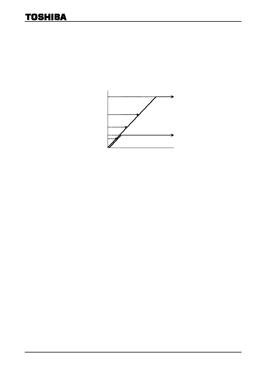
Note, however, that the conditions apply only to the case where the device is mounted on board A (180 mm
◊
125 mm
◊
1.6 mm, one-sided); board B (329 mm
◊
249 mm
◊
1.6 mm, two-sided); or board C (276 mm
◊
192 mm
◊
1.6 mm, six-layered). When mounting the IC, select boards no smaller than these. When using
under the conditions of board A, set the IC's power supply voltage (pins 19, 40, 55) to 8.8 V (
±
0.3 V)
Because the IC's thermal capacity margin is narrow, when designing a set, incorporate heat discharge
features into the design. Note that the power dissipation varies widely depending on the board mounting
conditions.
Note 2: Pins 3, 4, 5, 7, 8, 9, 10, 11, 20, 21, 22, 23, 30, 31, 33, 34, 36, 39, 45, 46, 49, 50, 51, 52 and 53 are
susceptible to damage from surge voltages and should thus be handled with extreme care.
Figure 1 Characteristics of decrease in power dissipation
Ambient temperature Ta (∞C)
P
o
wer
dissi
pati
on P
D
(mW
)
2717
0
150
25 65
1848
0
2297
3378
Printed circuit board B
Printed
circuit
board A
2551
1735
Printed circuit board C
TA1316AN
2002-10-04
34
Note 3: Power supply sequence
At power-on, power should be supplied to the IC's power supply pins according to the following sequence:
first to pin 29 (I
2
L V
DD
), then to pin 19 (DEF/DAC V
CC
), and finally to pin 40/pin 55 (RGB V
CC
/YC V
CC
).
Power to pin 29 should be supplied from pin 19 via zener diode through resister.
If power is not supplied to all the power pins or if power is not supplied in the above sequence, BUS preset
will be unsettled and the IC may not function properly.
Especially, when the frequency of H-out (pin 26) will be unsettled, H deflection output transistor may be
broken.
When this IC will be used on CRT, the frequency of H-out should be controlled by pin 22.
t
Figure (Note 3) Timing from immediately after power-on to time
at which H-out is output (at Ta
=
=
=
= 25∞∞∞∞C)
I
2
L V
DD
Logic operation 1.5 V (typ.)
Power-on reset (POR) threshold voltage
for bus operation 3.3 V (typ.)
H-out output 5.2 V (typ.)
V DEF/DAC
V
CC
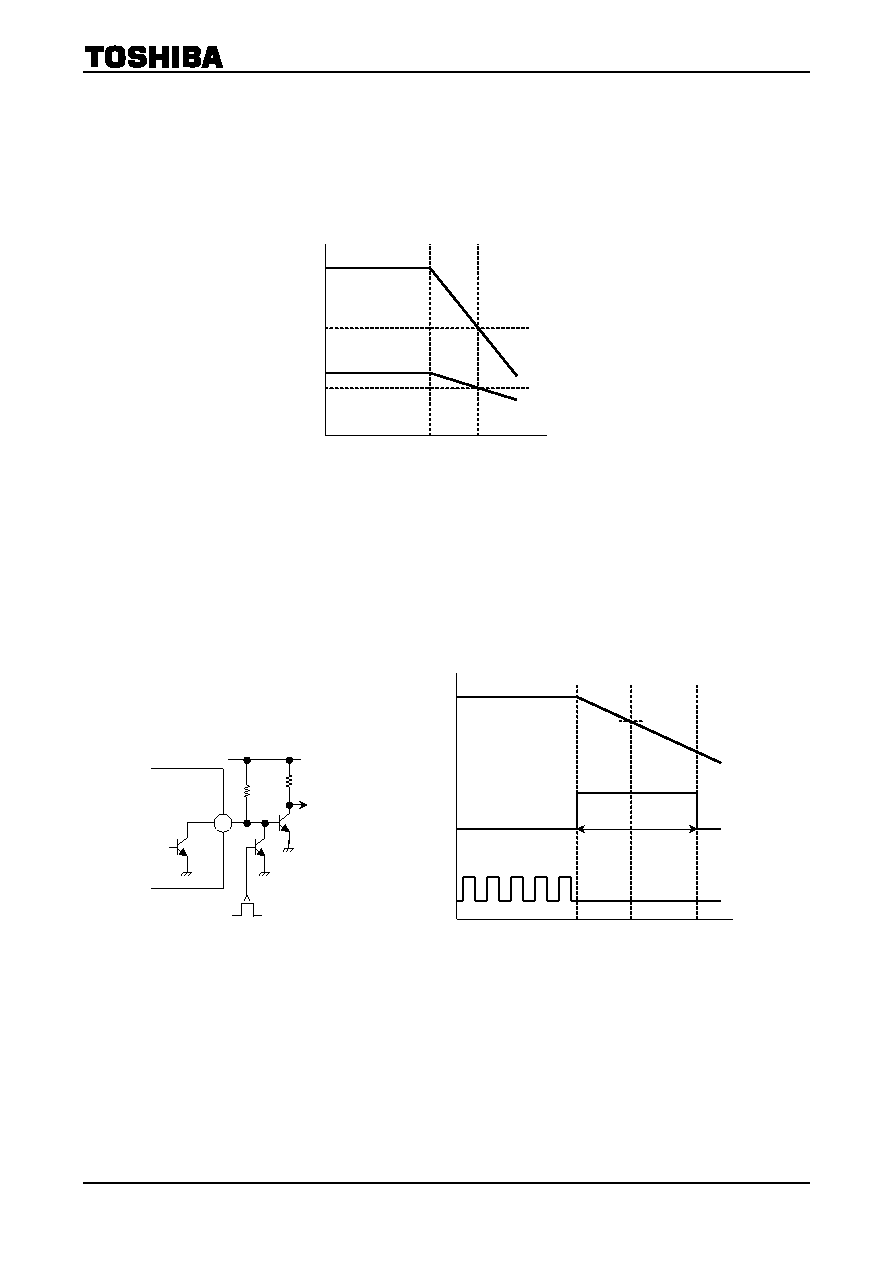
TA1316AN
2002-10-04
35
Note 4: V
CC
condition at Power-OFF
At power-off, the last pulse of H-out (pin 26) will become unknown, if I
2
L V
DD
(pin 29) is over 1.7 V at the
timing of H-out stop.
I
2
L V
DD
should be below 1.7 V when DEF/DAC V
CC
(pin 19) will be 6.2 V, which is the maximum voltage
when H-out stops.
Refer to Figure (Note 4-1).
If it is not in the condition of Figure (Note 4-1), it is recommended that H-out will be made LOW at power-off
by external control like micro-processor ang so on. Refer to Figure (Note 4-2).
Figure (Note 4-1) V
CC
condition at power-off
6.2 V
t
I
2
L V
DD
(pin 29)
V DEF/DAC V
CC
(pin 19)
H-out stop voltage (max)
below 1.7 V
Po
w
e
r
o
f
f
H-out
st
op
TA1316
26
DEF V
CC
H-out
Control signal by
micro-processor and so on.
H-out waveform
Approximately ten
milli seconds or more
Control signal by micro-processor and so on.
6.2 V
DFF/DAC V
CC
(Pin 19)
Po
w
e
r
O
F
F
H-out
st
op
t
Figure (Note 4-2) Example how to stop H-out
TA1316AN
2002-10-04
36
Recommended Operating Conditions
Characteristics Description
Min
Typ.
Max
Unit
Board
A
(Note1)
8.5 8.8 9.1
Pins 19, 40 and 55
Boards B and C (Note1)
8.7
9.0
9.3
Supply voltage (V
CC
)
Pin
29
1.8 2.0 2.2
V
Y input level
Pins 3 and 8: 100% color bar, including sync (picture
signal: 0.7 V
p-p
)
1.0
Color difference signal input level
Pins 4, 5, 9 and 10: 100% color bar, no sync
0.7
V
p-p
Matrix switching voltage
Pin 7
2.0
3.0
5.0
V
HD/VD input level
Pins 12, 13, 15 and 16
2.0
5.0
9.0
SYNC input level
Pin 14: 100% color bar, including sync
0.9
1.0
1.1
V
p-p
CP
4.7 5.0 9.0
SCP input level
Pin 17
BPP
2.2 2.5 2.8
15.75
kHz
8.0 9.0 9.0
31.5
kHz
5.0 6.0 7.0
33.75
kHz
2.0 3.0 4.0
Horizontal frequency switching
voltage
Pin 22
45 kHz
0
0
1.0
H-AFC
4.0 5.0 9.0
FBP input level
Pin 24
H-BLK 1.7
2.25
2.8
V
H-OUT input current
Pin 26
9.0 15.0
DAC input current
Pins 28 and 36
0.3 1.0
mA
SCL/SDA pull-up voltage
Pins 30 and 31
3.3
5.0
9.0
V
SDA input current
Pin 31
2 mA
Analog RGB input level
Pins 35, 34 and 33: White 100%
0.7
Analog OSD input level
Pins 37, 38 and 39: White 100%
0.7
V
p-p
Y
S
3
switching
voltage
Pin
49
1.5 5.0 9.0
OSD
2.9 5.0 9.0
Y
S
1/2 switching voltage
Pins 51 and
50
VSM
MUTE
1.1 1.5 1.7
BLK
7.0 9.0 9.0
P-MUTE
2.7 3.2 4.0
Y
M
switching voltage
Pin 52
HALF
TONE
1.2 1.5 1.8
V
External V-BLK input current
Pin 27
0.78
1 mA
Note1: For the parameter values for boards A, B and C, please refer to the table entitled Maximum Ratings.
Electrical Characteristics
(V
CC
=
=
=
= 9 V/2 V, Ta ==== 25∞C, unless otherwise specified)
Current Dissipation
Pin Name
Symbol
Test
Circuit
Min Typ. Max Unit
DEF/DAC V
CC
I
CC1
21.0 24.2 26.9
RGB V
CC
I
CC2
55.3 63.6 70.8
I
2
L V
DD
I
CC3
21.0 24.1 26.8
Y/C V
CC
I
CC4
39.3 45.3 50.3
mA
TA1316AN
2002-10-04
37
Pin Voltage
Test Condition
(1) BUS
= Preset
(2) SW1
= B, SW2 = B, SW3 = C, SW4 = B, SW5 = B, SW7 = A, SW8~10 = B, SW14 = B, SW20 = ON,
SW23 = B, SW24 = A, SW26 = A, SW33~35 = A, SW37~39 = A, SW54 = OFF, SW56 = ON
Pin No.
Pin Name
Symbol
Test
Circuit
Min Typ. Max Unit
2 BPH
FILTER
V
2
5.5 5.8 6.1
3 Y1
IN
V
3
4.7 5.0 5.3
4 Cb/Pb1
IN
V
4
4.7 5.0 5.3
5 Cr/Pr1
IN
V
5
4.7 5.0 5.3
7 MATRIX
SW
V
7
2.0 3.0 4.0
8 Y2
IN
V
8
4.7 5.0 5.3
9 Cb/Pb2
IN
V
9
4.7 5.0 5.3
10 Cr/Pr2
IN
V
10
4.7 5.0 5.3
11 COLOR
LIMITER
V
11
6.65 6.9 7.15
12 VD2
IN
V
12
0 0 0.3
13 HD2
IN
V
13
0 0 0.3
14 SYNC
IN
V
14
1.6 2.0 2.4
15 VD1
IN
V
15
0 0 0.3
16 HD1
IN
V
16
0 0 0.3
17 SCP
IN
V
17
3.9 4.4 4.9
20 AFC
FILTER
V
20
5.8 6.5 7.2
21 HVCO
V
21
5.0 5.3 5.6
23 H
CURVE
CORRECTION
V
23
2.2 2.5 2.8
33
ANALOG B IN
V
33
3.65 3.95 4.25
34 ANALOG
G
IN
V
34
3.65 3.95 4.25
35 ANALOG
R
IN
V
35
3.65 3.95 4.25
37
ANALOG OSD B IN
V
37
3.65 3.95 4.25
38 ANALOG
OSD
G
IN
V
38
3.65 3.95 4.25
39
ANALOG OSD R IN
V
39
3.65 3.95 4.25
46 B
S/H
V
46
3.5 4.0 4.5
47 G
S/H
V
47
3.5 4.0 4.5
48 R
S/H
V
48
3.5 4.0 4.5
49 Y
S
3 V
49
0.0 0.1 0.2
50 Y
S
2 V
50
0.0 0.1 0.2
51 Y
S
1 V
51
0.0 0.1 0.2
52 Y
M
V
52
0.0 0.1 0.2
53 ABCL
IN
V
53
5.85 6.1 6.35
54 VSM
OUT
V
54
4.2 4.4 4.6
56 APL
FILTER
V
56
4.8 5.0 5.2
V
TA1316AN
2002-10-04
38
Luminance Block
Characteristics
Symbol
Test
Circuit
Test Condition
Min
Typ.
Max
Unit
Y input dynamic range
D
RY
0.7
1.0
1.5
V
p-p
V
B
-15
-5
5
Black detection level shift
V
B3
(Note P01)
35
45
55
mV
Black stretch amplifier maximum gain
G
BS
(Note P02)
2.5
3.0
3.5
dB
P
BST1
31
34
37
Black stretch start point 1
P
BST2
(Note P03)
50
53
56
IRE
P
BS1
0
5
10
Black stretch start point 2
P
BS2
(Note P04)
19
24
29
IRE
DV
001
30
50
70
DV
010
80
100
120
Dynamic ABL detection voltage
DV
100
(Note P05)
190
220
250
mV
S
DAMIN
0.005
0.02
Dynamic ABL sensitivity
S
DAMAX
(Note P06)
0.29
0.32
0.35
V/V
Black level correction
BLC
(Note P07)
7.0
8.5
10
IRE
P
DGP00
17
20
23
P
DGPA
0.5
1.5
2.5
P
DGPB
2
3.5
5
Dynamic Y
correction point
P
DGPC
(Note P08)
3
5
7
IRE
Dynamic Y
gain
G
DG
(Note P09)
2
3
4
dB
Static Y
dark area gain
G
SG
(Note P10)
1.3
1.7
2.2
dB
ADT
100
0.9
1.1
1.2
ADT
135
1.2
1.35
1.5
DC restoration gain
ADT
65
(Note P11)
0.55
0.7
0.85
times
V
DT0
-5
0
5
DC restoration start point
V
DT1
(Note P12)
47
51
55
%
P
DTL11
54
57
61
P
DTL10
67
71
75
P
DTL01
74
78
82
DC restoration limit point
P
DTL00
(Note P13)
74
78
82
%
F
AP00
12.2
13.5
14.9
F
AP01
8.5
9.5
10.5
F
AP10
6.5
7.3
8.1
Sharpness control peak frequency
F
AP11
4.2
4.7
5.2
MHz
G
MAX00
13
16
18
G
MIN00
-15
-8
-4
G
MAX01
14
17
19
G
MIN01
-20
-14
-7
G
MAX10
14
17
19
G
MIN10
-25
-16
-7
G
MAX11
14
18
20
Sharpness control range
G
MIN11
(Note P14)
-30
-20
-8
dB
TA1316AN
2002-10-04
39
Characteristics
Symbol
Test
Circuit
Test Condition
Min
Typ.
Max
Unit
G
CEN00
7.5
10
12.5
G
CEN01
8
11
13
G
CEN10
8
11
13
Sharpness control center
characteristic
G
CEN11
(Note P15)
9
12
14
dB
G
YNRT00
-15
-8
-4
G
YNRF00
-3
-1
1
G
YNRT01
-20
-12
-8
G
YNRF01
-3
-1
1
G
YNRT10
-20
-13
-8
G
YNRF10
-2
-0.5
1.5
G
YNRT11
-25
-12
-8
YNR characteristic
G
YNRF11
(Note P16)
-2
0
2
dB
T
SRT00
0.05
0.4
0.7
T
SRT01
0.5
1
2
T
SRT10
1.5
2
4
Control of SRT response to 2T pulse
input
T
SRT11
(Note P17)
3.5
5
7
dB
VSM peak frequency
F
VSM
15
19
22.8
MHz
G
V000
-39
-35
G
V001
2
3
4
G
V010
5.5
6.5
7.5
G
V011
9.5
11
12
G
V100
12.5
13.8
15
G
V101
14.5
16
17.5
G
V110
15.5
16.8
18.5
VSM gain
G
V111
(Note P18)
17.5
18.6
19.5
dB
V
SR49
0.62
0.72
0.85
V
SR50
0.62
0.72
0.85
Threshold voltage of VSM muting
V
SR51
Pins 49, 50 and 51
0.62
0.72
0.85
V
T
VM49A
0
30
100
T
VM49B
0
30
100
T
VM50A
0
30
100
T
VM50B
0
30
100
T
VM51A
0
30
100
Response time for VSM muting
T
VM51B
(Note P19)
0
30
100
ns
V
LU
0.58
0.65
0.75
VSM limit
V
LD
(Note P20)
0.55
0.62
0.75
V
p-p
Delay time from Y input to R output
T
YR
(Note P21)
96
120
144
ns
YDLA
3
5
7
YDLB
7
10
13
Y delay time switch
YDLC
(Note P22)
11
15
19
ns
G
AMIN
-5
-3.2
-2.0
G
BMIN
1
2
3.5
G
AMAX
0.3
1.0
1.7
Transfer distortion correction
G
BMA X
(Note P23)
-3.0
-1.5
-1.0
dB
TA1316AN
2002-10-04
40
Characteristics
Symbol
Test
Circuit
Test Condition
Min
Typ.
Max
Unit
G
CDE00
5.5
6.8
8
G
CDE01
5.5
6.8
8
G
CDE10
5.5
6.8
8
Color detail enhancer
G
CDE11
(Note P24)
5.5
6.8
8
dB
F
YD00
4.4
5.5
6.6
F
YD01
2.9
3.7
4.5
F
YD10
11.6
14.5
17.4
Y detail frequency
F
YD11
8
10
12
MHz
G
YDMAX00
6
9
12
G
YDMAX01
7
10
13
G
YDMAX10
2.5
5.5
8.5
G
YDMAX11
3
6
9
G
YDCEN00
3.5
6.5
9.5
G
YDCEN01
4
7
10
G
YDCEN10
-2
0.8
2
G
YDCEN11
-1
1
2
G
YDMIN00
0
1.5
3
G
YDMIN01
0
2
4
G
YDMIN10
-8
-5
-2
Y detail control range
G
YDMIN11
(Note P25)
-18
-15
-12
dB
G
WPL1
-10
-7
-4
G
WPL2
-7
-4.8
-2
APACON white peak limiter
G
WPL3
(Note P26)
-5
-2.3
-0.5
dB
TA1316AN
2002-10-04
41
Color Difference 1/YUV Input and Matrix Block
Characteristics
Symbol
Test
Circuit
Test Condition
Min
Typ.
Max
Unit
D
BB
0.7
0.9
1
Color difference signal input dynamic
range
D
RR
0.7
0.9
1
V
p-p
T
RMAX
25
29
33
T
RMIN
-37
-33
-29
T
BMAX
27
31
35
Color difference signal tint control
characteristic
T
BMIN
-36
-32
-28
∞
Matrix fast SW threshold voltage
V
MSW
Pin 7
0.65
0.72
0.8
V
F
B00
3.6
4.5
5.4
F
B01
4.6
5.8
7.0
F
B10
6.8
8.5
10.2
F
R00
3.6
4.5
5.4
F
R01
4.6
5.8
7.0
Color SRT peak frequency
F
R10
6.8
8.5
10.2
MHz
GS
B00CEN
5
8
11
GS
B00MAX
9
12
15
GS
B01CEN
2
5
8
GS
B01MAX
5
8
11
GS
B10CEN
1
2
5
GS
B10MAX
1
3
6
GS
R00CEN
5
8
11
GS
R00MAX
9
12
15
GS
R01CEN
2
5
8
GS
R01MAX
5
8
11
GS
R10CEN
1
2
5
Color SRT gain
GS
R10MAX
(Note S01)
1
3
6
dB
Delay time from Cb1 input to B output
T
B
104
130
156
Delay time from Cr1 input to R output
T
R
104
130
156
ns

TA1316AN
2002-10-04
42
Characteristics
Symbol
Test
Circuit
Test Condition
Min
Typ.
Max
Unit
GC
BDY1
0.3
0.5
0.7
GC
BDY2
0.7
1.0
1.3
GC
BDY3
0.7
1.0
1.3
GC
BBS1
0.2
0.4
0.6
GC
BBS2
-1.0
-0.6
-0.5
GC
BBS3
-3.6
-3.3
-3.0
GC
RDY1
0.3
0.5
0.7
GC
RDY2
1.4
1.6
1.8
GC
RDY3
1.4
1.6
1.8
GC
RBS1
0.1
0.3
0.5
GC
RBS2
-1.2
-1.0
-0.8
Color difference signal amplitude
correction
GC
RBS3
(Note S02)
-3.7
-3.3
-2.9
dB
G
Y00
4.5
5.5
6
G
Y01
4.5
5.5
6
G
Y10
4.5
5.5
6
G
Y11
4.5
5.5
6
G
BA
0.2
0.4
0.5
G
BB
1.0
1.1
1.3
G
BC
1.0
1.1
1.3
G
RA
0.8
1.0
1.2
G
RB
-1.6
-1.4
-1.2
YUV gain
G
RC
(Note S03)
-3.4
-3.2
-3.0
dB

TA1316AN
2002-10-04
43
Color Difference 2 Block
Characteristics
Symbol
Test
Circuit
Test Condition
Min
Typ.
Max
Unit
Color difference signal contrast
adjustment characteristic
V
uCY
(Note A01)
15.5
17.0
18.5
dB
v
cCY
+
3.6
4.6
5.6
Color adjustment characteristic
vcCY-
(Note A02)
-35
-25
-18
dB
RMAX
109
111.5
114
RCNT
98.5
101
103.5
RMIN
88
90
92
∞
V
R
/V
BMAX
0.82
0.85
0.88
V
R
/V
BCNT
0.68
0.71
0.74
R-Y relative phase and amplitude
V
R
/V
BMIN
0.51
0.54
0.57
times
GMAX
253
256
259
GCNT
245
248
251
GMIN
229
232
235
∞
V
G
/v
BMAX
0.35
0.38
0.41
V
G
/v
BCNT
0.30
0.33
0.36
G-Y relative phase and amplitude
V
G
/v
BMIN
0.25
0.28
0.31
times
GHT
RY
0.47
0.50
0.53
GHT
GY
0.47
0.50
0.53
Color difference signal half-tone
characteristic
GHT
BY
(Note A03)
0.47
0.50
0.53
times
V
1
0.09
0.23
0.37
V
2
0.26
0.40
0.54
V
3
0.44
0.58
0.72
V
p-p
Color
characteristic
(Note A04)
0.60
0.70
0.80
CLT
0
1.45
1.65
1.85
Color limiter characteristic
CLT
1
(Note A05)
1.80
2.00
2.20
V
p-p
High bright color gain
HBC
1
(Note A06)
0.02
0.04
0.06
times

TA1316AN
2002-10-04
44
Text Block
Characteristics
Symbol
Test
Circuit
Test Condition
Min
Typ.
Max
Unit
G
R
3.39
3.80
4.28
G
G
3.39
3.80
4.28
AC gain
(Y1in~R/G/B out)
G
B
(Note T01)
3.39
3.80
4.28
times
G
G/R
0.94
1.00
1.06
AC gain axial difference
G
B/R
0.94
1.00
1.06
G
fR
24
30
G
fG
24
30
Frequency characteristic
(Y1in~R/G/B out)
G
fB
Flat gain
(-3 dB point at 10 MHz)
24
30
MHz
G
fCb
11
14.5
Frequency characteristics
(Cb1/Cr1in~R/G/B out)
G
fCr
11
14.5
MHz
Unicolor adjustment characteristic
V
u
(Note T02)
15.5
16.5
17.5
dB
V
brMAX
4.10
4.45
4.80
V
brCNT
3.05
3.40
3.75
Brightness adjustment characteristic
V
brMIN
(Note T03)
1.95
2.30
2.65
V
V
wps1
2.30
2.45
2.65
White peak slice level
V
wps2
(Note T04)
2.70
2.90
3.10
V
p-p
Black peak slice level
V
bps
(Note T05)
1.05
1.20
1.35
V
N
41
-55
-49
N
42
-55
-49
RGB output S/N
N
43
(Note T06)
-55
-49
dB
G
HT1
0.45
0.50
0.55
Half-tone characteristic
G
HT2
(Note T07)
0.45
0.50
0.55
times
Half-tone ON voltage
V
HT
Pin 52
0.65
0.85
1.05
V
V
VR
0.30
0.80
1.30
V
VG
0.30
0.80
1.30
Vertical blanking pulse output level
V
VB
0.30
0.80
1.30
V
V
HR
0.30
0.80
1.30
V
HG
0.30
0.80
1.30
Horizontal blanking pulse output level
V
HB
0.30
0.80
1.30
V
td
ON
0.00
0.30
Blanking pulse delay time
td
OFF
(Note T08)
0.08
0.30
µs
v
su
+
2.1
2.6
3.1
Sub-contrast variable range
v
su
-
-4.0
-3.5
-3.0
dB
CUT
+
0.42
0.47
0.52
Cutoff voltage variable range
CUT
-
0.42
0.47
0.52
V
TA1316AN
2002-10-04
45
Characteristics
Symbol
Test
Circuit
Test Condition
Min
Typ.
Max
Unit
DR
R1
+
2.5
3.0
3.5
DR
R1
-
-5.5
-5.0
-4.5
DR
R2
+
2.5
3.0
3.5
DR
R2
-
-5.5
-5.0
-4.5
DR
G1
+
2.5
3.0
3.5
DR
G1
-
-5.5
-5.0
-4.5
DR
G2
+
2.5
3.0
3.5
DR
G2
-
-5.5
-5.0
-4.5
DR
G3
+
2.5
3.0
3.5
DR
G3
-
-5.5
-5.0
-4.5
DR
B1
+
2.5
3.0
3.5
DR
B1
-
-5.5
-5.0
-4.5
DR
B2
+
2.5
3.0
3.5
DR
B2
-
-5.5
-5.0
-4.5
DR
B3
+
2.5
3.0
3.5
Drive adjustment variable range
DR
B3
-
(Note T09)
-5.5
-5.0
-4.5
dB
MU
RD
1.5
1.7
1.9
MU
GD
1.5
1.7
1.9
Output voltage at picture muting
MU
BD
1.5
1.7
1.9
V
P mute ON voltage
V
MUTE
Pin 52
1.90
2.15
2.40
V
BB
R
1.0
1.2
1.4
BB
G
1.0
1.2
1.4
V
Output voltage at blue back
BB
B
1.1
1.25
1.4
V
p-p
Pin 53 input impedance
Zin
(Note T10)
24
30
36
k
ACL
1
-7.5
-5.5
-3.5
ACL characteristic
ACL
2
(Note T11)
-16.0 -14.5 -12.0
dB
ABL
P1
0.10
0.15
0.20
ABL
P2
-0.01 0.04
0.09
ABL
P3
-0.07 -0.02 0.03
ABL
P4
-0.17 -0.12 -0.07
ABL
P5
-0.27 -0.22 -0.17
ABL
P6
-0.36 -0.31 -0.26
ABL
P7
-0.44 -0.39 -0.34
ABL point
ABL
P8
(Note T12)
-0.50 -0.45 -0.40
V
ABL
G1
-0.06 -0.02 0.00
ABL
G2
-0.17 -0.12 -0.07
ABL
G3
-0.34 -0.29 -0.24
ABL
G4
-0.52 -0.47 -0.42
ABL
G5
-0.68 -0.63 -0.59
ABL
G6
-0.85 -0.80 -0.75
ABL
G7
-1.01 -0.96 -0.91
ABL gain
ABL
G8
(Note T13)
-1.09 -1.04 -0.99
V
TA1316AN
2002-10-04
46
Characteristics
Symbol
Test
Circuit
Test Condition
Min
Typ.
Max
Unit
V
43R
2.15
2.40
2.65
V
42R
0.30
0.80
1.30
V
41R
0.30
0.80
1.30
V
43G
0.30
0.80
1.30
V
42G
2.15
2.40
2.65
V
41G
0.30
0.80
1.30
V
43B
0.30
0.80
1.30
V
42B
0.30
0.80
1.30
RGB output mode
V
41B
(Note T14)
2.15
2.40
2.65
V
1
56
66
76
2
72
82
92
IRE
1
0.49
1.24
1.99
2
-1.67 -0.92 -0.17
Y-OUT
characteristic
3
(Note T15)
-4.59 -3.84 -3.09
dB
BS
Pmin
55.0
60.0
65.0
BS
Pcnt
92.5
97.5
102.5
BS
Pmax
107
112
117
IRE
BS
Gmin
1.75
2.25
2.75
BS
Gcnt
6.4
7.4
8.4
Blue stretch circuit characteristic
BS
Gmax
(Note T16)
9
10
11
dB
Forced blanking input threshold
voltage
V
BLKIN
Pin 52
5.50
6.00
6.50
V
ACBR
1
ACBG
2
ACBB
3
H
V
ACB1R
0.04
0.07
0.10
V
ACB1G
0.04
0.07
0.10
V
ACB1B
0.04
0.07
0.10
V
ACB2R
0.16
0.21
0.26
V
ACB2G
0.16
0.21
0.26
V
ACB2B
0.16
0.21
0.26
V
ACB3R
0.41
0.46
0.51
V
ACB3G
0.41
0.46
0.51
ACB pulse phase and amplitude
V
ACB3B
(Note T17)
0.41
0.46
0.51
V
p-p
IK
R
0.73
0.93
1.13
IK
G
0.73
0.93
1.13
IK input amplitude
IK
B
(Note T18)
0.73
0.93
1.13
V
p-p
DIK
in
+
3.00
3.30
3.60
IK input cover range
DIK
in
-
(Note T19)
-0.50 -0.30 -0.10
V
TA1316AN
2002-10-04
47
Characteristics
Symbol
Test
Circuit
Test Condition
Min
Typ.
Max
Unit
G
TXR
3.03
3.40
3.83
G
TXG
3.03
3.40
3.83
Analog RGB gain
G
TXB
(Note T20)
3.03
3.40
3.83
times
G
TXG/R
0.94
1.00
1.06
Analog RGB gain triaxial difference
G
TXB/R
0.94
1.00
1.06
Gf
TXR
30
35
Gf
TXG
30
35
Analog RGB frequency characteristic
Gf
TXB
At
-3dB
30
35
MHz
DR
35
0.80
1.20
1.50
DR
34
0.80
1.20
1.50
Analog RGB input dynamic range
DR
33
0.80
1.20
1.50
V
p-p
TXV
WPSR
2.30
2.55
2.80
TXV
WPSG
2.30
2.55
2.80
Analog RGB white peak slice level
TXV
WPSB
(Note T21)
2.30
2.55
2.80
V
p-p
V
BPSR
1.05
1.20
1.35
V
BPSG
1.05
1.20
1.35
Analog RGB black peak limit level
V
BPSB
(Note T22)
1.05
1.20
1.35
V
v
uTXR
15.5
16.5
18.5
v
uTXG
15.5
16.5
18.5
RGB contrast adjustment
characteristic
v
uTXB
(Note T23)
15.5
16.5
18.5
dB
V
brTXmax
3.0
3.2
3.4
V
brTXcnt
2.5
2.7
2.9
Analog RGB brightness adjustment
characteristic
V
brTXmin
(Note T24)
2.0
2.2
2.4
V
Analog RGB mode switch voltage
V
TXON
Pin 49
0.65
0.85
1.05
V
RYS
15
50
tP
RYS
20
50
t
RYS
0
10
FYS
10
50
tP
RYS
30
50
Analog RGB mode switching transfer
characteristic
t
RYS
(Note T25)
0
10
ns
TXACL
1
-2.00 -1.00 -0.05
TXACL
2
-7.5
-5.5
-3.5
TXACL
3
-6.0
-4.0
-2.0
Text ACL characteristic
TXACL
4
(Note T26)
-17
-15
-13
dB
G
OSDR
2.95
3.30
3.70
G
OSDG
2.95
3.30
3.70
Analog OSD gain
G
OSDB
(Note T27)
2.95
3.30
3.70
times
G
OSDG/R
0.94
1.00
1.06
Analog OSD gain triaxial difference
G
OSDB/R
0.94
1.00
1.06
TA1316AN
2002-10-04
48
Characteristics
Symbol
Test
Circuit
Test Condition
Min
Typ.
Max
Unit
Gf
OSDR
35
40
Gf
OSDG
35
40
Analog OSD frequency characteristic
Gf
OSDB
At
-3dB
35
40
MHz
DR
35
0.80
1.20
1.50
DR
34
0.80
1.20
1.50
Analog OSD input dynamic range
DR
33
0.80
1.20
1.50
V
p-p
OSDV
WPSR
2.45
2.70
2.95
OSDV
WPSG
2.45
2.70
2.95
Analog OSD input white peak slice
level
OSDV
WPSB
(Note T28)
2.45
2.70
2.95
V
p-p
OSDV
BPSR
1.30
1.45
1.60
OSDV
BPSG
1.30
1.45
1.60
Analog OSD input black peak limit
level
OSDV
BPSB
(Note T29)
1.30
1.45
1.60
V
V
UOSDR11
0.58
0.64
0.71
V
UOSDG11
0.58
0.64
0.71
V
UOSDB11
0.58
0.64
0.71
V
UOSDR10
0.47
0.53
0.59
V
UOSDG10
0.47
0.53
0.59
V
UOSDB10
0.47
0.53
0.59
V
UOSDR01
0.32
0.38
0.46
V
UOSDG01
0.32
0.38
0.46
V
UOSDB01
0.32
0.38
0.46
V
UOSDR00
0.21
0.23
0.25
V
UOSDG00
0.21
0.23
0.25
Analog OSD contrast adjustment
characteristic
V
UOSDB00
(Note T30)
0.21
0.23
0.25
V
p-p
V
brOSD0
2.20
2.40
2.60
V
brOSD1
2.05
2.25
2.45
V
brOSD2
1.95
2.15
2.35
Analog OSD brightness adjustment
characteristic
V
brOSD3
(Note T31)
1.80
2.00
2.20
V
V
OSDON1
Pin 51
2.05
2.30
2.55
Analog OSD mode switch voltage
V
OSDON2
Pin 50
2.05
2.30
2.55
V
TA1316AN
2002-10-04
49
Characteristics
Symbol
Test
Circuit
Test Condition
Min
Typ.
Max
Unit
RYS1
15
50
tP
RYS1
20
50
tP
RYS1
0
10
FYS1
10
50
tP
RYS1
30
50
tP
RYS1
0
10
RYS2
15
50
tP
RYS2
20
50
tP
RYS2
0
10
FYS2
10
50
tP
RYS2
30
50
tP
RYS2
0
10
t
ROSD
20
50
tP
ROSD
15
50
tP
ROSD
0
10
FOSD
20
50
tP
ROSD
20
50
Analog OSD mode switching transfer
characteristic
tP
ROSD
(Note T32)
0
10
ns
OSDACL
1
0.00
OSDACL
2
0.00
OSDACL
3
-8.0
-5.5
-3.0
OSD ACL characteristic
OSDACL
4
(Note T33)
-17
-15
-13
dB
41TV
1
-7
-6
-5
42TV
1
-7
-6
-5
43TV
1
-7
-6
-5
41TV
2
-4
-3
-2
42TV
2
-4
-3
-2
43TV
2
-4
-3
-2
41TV
3
-55
-50
42TV
3
-55
-50
43TV
3
-55
-50
41OSD
1
-6.5
-5.5
-4.5
42OSD
1
-6.5
-5.5
-4.5
43OSD
1
-6.5
-5.5
-4.5
41OSD
2
-12.0 -10.5 -9.0
42OSD
2
-12.0 -10.5 -9.0
43OSD
2
-12.0 -10.5 -9.0
41OSD
3
-40
-30
42OSD
3
-40
-30
OSD blending characteristic
43OSD
3
(Note T34)
-40
-30
dB
Crosstalk between inputs
-50
-40
dB
TA1316AN
2002-10-04
50
Deflection Block
Parameter
Symbol
Test
Circuit
Test Condition
Min
Typ.
Max
Unit
Sync input horizontal sync phase
S
PH
(Note HA01)
0.55
0.65
0.75
µs
HD 1/2 input horizontal sync phase
HD
1PH/2PH
(Note HA02)
0.58
0.68
0.78
µs
HD
DUTY1
0.5
2.0
HD
DUTY2
62
67
72
HD
DUTY3
99.5
98
Polarity detection range
HD
DUTY4
(Note HA03)
47.5
52.5
57.5
%
V
thS00
4
8.5
14
V
thS01
14
20
26
V
thS10
24
30
36
Sync input threshold amplitude
V
thS11
(Note HA04)
34
40
46
%
HD 1/2 input threshold voltage
V
thHD1/2
(Note HA05)
0.7
0.8
0.9
V
p-p
H
SFT
-
9.5
10.5
11.5
Horizontal picture phase adjustment
variable range
H
SFT
+
(Note HA06)
9.5
10.5
11.5
%
Curve correction amount
H
#23
(Note HA07)
2.9
3.4
3.9
%
CP
S0
3.1
3.8
4.5
CP
W0
2.0
2.5
3.0
%
CP
V0
4.7
5.0
5.3
V
CP
S1
0
0.7
1.5
CP
W1
1.9
2.4
2.9
%
CP
V1
4.7
5.0
5.3
V
CP
S2
3.2
4.2
5.2
CP
W2
2.2
2.7
3.2
%
Clamp pulse phase, width and level
CP
V2
(Note HA08)
4.7
5.0
5.3
V
HBP
S0a
4.3
6.3
8.9
HBP
S0b
4.3
6.3
8.9
%
HBP
V0
2.2
2.5
2.8
V
HBP
S1a
1.5
3.5
5.9
HBP
S1b
1.5
3.5
5.9
%
HBP
V1
2.2
2.5
2.8
V
HBP
s45a
6.0
8.5
11.5
%
HBP
s45b
6.0
8.5
11.5
%
Black peak detection pulse phase and
level
HBP
sv45
(Note HA09)
2.2
2.5
2.8
%
FBP threshold
V
thFBP
(Note HA10)
2.5
3.0
3.5
V
HVCO oscillation start voltage
V
VCO
Monitor pin 21
= V
CC
3.5
4.0
4.5
V
H-OUT start voltage
V
HON
Monitor pin 26
= V
CC
4.5
5.2
6.2
V
TA1316AN
2002-10-04
51
Parameter
Symbol
Test
Circuit
Test Condition
Min
Typ.
Max
Unit
TH
00A
39
41
43
TH
01A
38
40
42
TH
10A
38
40
42
TH
00B
45
47
49
TH
01B
44.5
46.5
48.5
H-OUT pulse duty
TH
10B
(Note HB01)
45
47
49
%
F00
15.59
15.75
15.91
F01
31.19
31.5
31.82
F10
33.41
33.75
34.09
Horizontal free-running frequency
F11
(Note HB02)
44.52
45.0
45.48
kHz
F00
MIN
14.48
14.78
15.08
F00
MAX
16.37
16.70
17.03
F01
MIN
28.97
29.56
30.15
F01
MAX
32.72
33.39
34.06
F10
MIN
30.91
31.54
32.17
F10
MAX
34.91
35.62
36.33
F11
MIN
43.20
44.00
44.80
Horizontal oscillation frequency
variable range
F11
MAX
(Note HB03)
47.85
48.65
49.45
kHz
BH00
176
220
264
BH01
352
440
528
BH10
376
470
564
Horizontal oscillation control sensitivity
BH11
Hz/0.1 V (Note HB04)
520
650
780
V26
H
4.8
5.1
5.2
H-OUT output voltage
V26
L
(Note HB05)
0.1
0.3
V
V22
L
1.3
1.5
1.7
V22
M
4.3
4.5
4.7
Horizontal oscillation frequency pin (pin
22) control voltage threshold
V22
H
7.3
7.5
7.7
VDAC
2H
TEST
= (00), DAC2 = (1)
8.5
9.0
DAC switching voltage
DAC2
VDAC
2L
TEST
= (00), DAC2 = (0)
0.3
0.7
V
VP output pulse width
VP
W
4
4.5
5
H
000
VPt0
1278
1281
1284
001
VPt1
846
849
852
010
VPt2
722
725
728
011
VPt3
657
660
663
100
VPt4
610
613
616
101
VPt5
360
363
366
Vertical free-running
(maximum pull-in range)
110
VPt6
(Note V01)
304
307
310
H
Vertical minimum pull-in range
T
VPULL
(Note V02)
47
48
49
H
TA1316AN
2002-10-04
52
Parameter
Symbol
Test
Circuit
Test Condition
Min
Typ.
Max
Unit
VBPP
0E
51
52
53
000
VBPP
0S
1099.5 1100.5 1101.5
VBPP
1E
51
52
53
001
VBPP
1S
729.5
730.5
731.5
VBPP
2E
49.5
50.5
51.5
010
VBPP
2S
599.5
600.5
601.5
VBPP
3E
49.5
50.5
51.5
011
VBPP
3S
544.5
545.5
546.5
VBPP
4E
51
52
53
100
VBPP
4S
499.5
500.5
501.5
VBPP
5E
51
52
53
101
VBPP
5S
289.5
290.5
291.5
VBPP
6E
51
52
53
Vertical black peak detection
pulse
110
VBPP
6S
(Note V03)
239.5
240.5
241.5
H
V
BLKMIN
15
16
17
Vertical blanking stop phase
V
BLKMAX
(Note V04)
45
46
47
H
High
V
27VPH
4.6
5.0
5.4
VP output voltage
Low
V
27VPL
Pin 27 voltage
0.1
0.5
V
15.75 kHz
10.0
11.6
13.4
31.5 kHz
4.8
5.8
7.6
33.75 kHz
4.4
5.4
7.2
Delay time from SYNC input to VP
output
45 kHz
3.1
4.1
5.9
µs

TA1316AN
2002-10-04
53
Parameter
Symbol
Test
Circuit
Test Condition
Min
Typ.
Max
Unit
CBLK1
000min
1087
1088
1089
000
CBLK1
000max
1117
1118
1119
CBLK1
001min
719
720
721
001
CBLK1
001max
749
750
751
CBLK1
010min
591
592
593
010
CBLK1
010max
621
622
623
CBLK1
011min
527
528
529
011
CBLK1
011max
557
558
559
CBLK1
100min
487
488
489
100
CBLK1
100max
517
518
519
CBLK1
101min
279
280
281
101
CBLK1
101max
309
310
311
CBLK1
110min
223
224
225
Compression BLK1
(start phase)
110
CBLK1
110max
253
254
255
H
CBLK2
000min
49
50
51
000
CBLK2
000max
77
78
79
CBLK2
001min
49
50
51
001
CBLK2
001max
77
78
79
CBLK2
010min
49
50
51
010
CBLK2
010max
77
78
79
CBLK2
011min
49
50
51
011
CBLK2
011max
77
78
79
CBLK2
100min
49
50
51
100
CBLK2
100max
77
78
79
CBLK2
101min
49
50
51
101
CBLK2
101max
77
78
79
CBLK2
110min
49
50
51
Compression BLK2
(stop phase)
110
CBLK2
110max
77
78
79
H
External vertical blanking insert
current
I
EXTBLK
Pin 27, current
520
625
780
µA
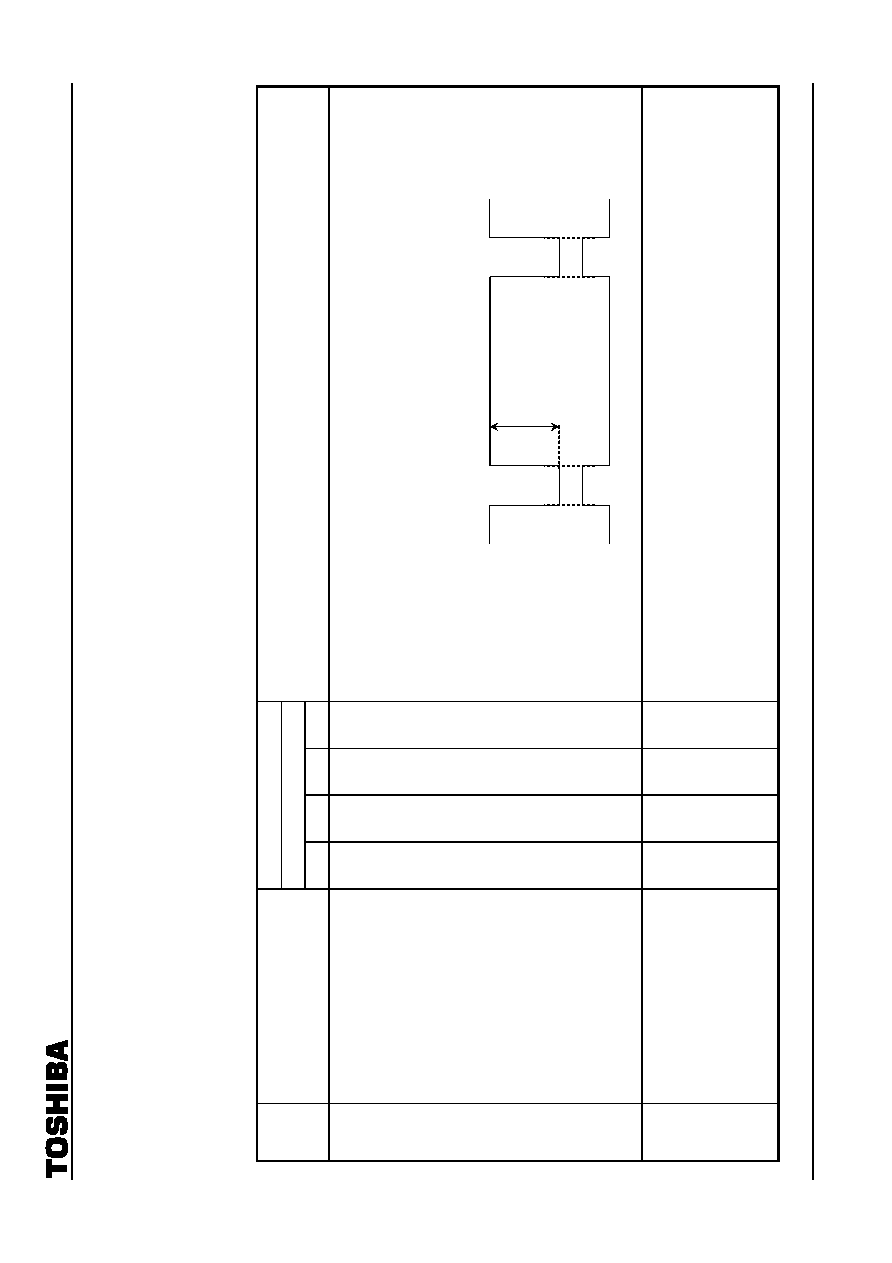
TA1316AN
2002-10-04
54
Test Conditions for Luminance
Common Test Conditions for Luminance
(1) SW4
= SW5 = B, SW7 = OPEN, SW8~SW10 = B, SW20 = ON, SW23 = B, SW33SW39 = A, SW54 = 54 = ON
(2) After sending bus control data with preset values, set ACB MODE to off (00) and SYNC INPUT-SW to sync input (10).
(3) Input sync signal [signal in sync with input signal used for testing, except for sweep signal] to pin 14 (SYNC IN). Set horizontal frequency to that of pin 14.
(4) Set pin 7 to open, Y/color difference signal input mode (YUV INPUT MODE) to Through (10), SYNC SEP-LEVEL to 20% (01) and vertical free-running frequency
to 307H (110).
Test Conditions
SW mode
Note No.
Parameter
SW1
SW2
SW3
SW56
Test Method (test conditions: V
CC
= 9 V/2 V, Ta
= 25∞ ± 3∞C)
P01
Black detection level shift
B
C
C
OPEN (1) Connect external power supply (PS) to pin 3 and monitor pins 2 and 56.
(2) Set black stretch point 1 to off (000) and black detection level (BDL) to 0 IRE (1).
(3) Increase PS voltage from 4.95 V in 1-mV steps. When pin 2 picture period (High) goes Low, measure pin 56
DC differential V
B
.
(4) Set black detection level (BDL) to 3 IRE (0).
(5) Repeat step (3) above and measure pin 56 DC differential V
B3
.
P02
Black stretch amplifier maximum gain
B
A
A
OPEN (1) Set SW2 to A (maximum gain) and input 500-kHz sine wave to TPA.
(2) Adjust signal amplitude to 0.1 V
p-p
using pin 3.
(3) Set black stretch point 1 to off (000) and measure pin 56 amplitude V
A
.
(4) Set black stretch point 1 to 001 (black stretch on) and measure pin 56 amplitude V
B
.
(5) Calculate GBS using the following formula.
GBS
= 20 ◊ og (V
B
˜ V
A
) [dB]
V
B
, V
B3
Pin 56 waveform
Pin 2 waveform

TA1316AN
2002-10-04
55
Test Conditions
SW mode
Note No.
Parameter
SW1
SW2
SW3
SW56
Test Method (test conditions: V
CC
= 9 V/2 V, Ta
= 25∞ ± 3∞C)
P03
Black stretch start point 1
B
A
C
OPEN (1) Set SW2 to A (maximum gain) and black stretch start point 1 to off (000).
(2) Connect external power supply (PS) to pin 3, increase voltage from V
3
, and plot resulting pin 56 voltage
change S1. Define pin 56 voltages when V
3
and V
3
+ 0.7 V are applied as V
0
and V
100
.
(3) Set black stretch start point 1 to 001 (minimum), increase PS voltage from V
3
as in (2) above and plot
resulting pin 56 voltage change S2.
(4) Set black stretch start point 1 to maximum (111), repeat step (2) above and plot resulting pin 56 voltage
change S3.
(5) Determine S1 and S2 intersection V
BST1
and S1 and S3 intersection V
BST2
using the graph below. Calculate
P
BST1
and P
BST2
using the following formulae.
V
Z
[V]
= V
100
[V]
- V
0
[V]
P
BST1
[(IRE)]
= [(V
BST1
[V]
- V
56
[V])
˜ V
Z
]
◊ 100 (IRE)
P
BST2
[(IRE)]
= [(V
BST2
[V]
- V
56
[V])
˜ V
Z
]
◊ 100 (IRE)
Pin 56
Pin 3
V
56
V
BST1
V
BST2
S3
S2
S1
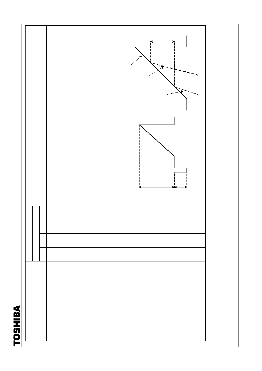
TA1316AN
2002-10-04
56
Test Conditions
SW mode
Note No.
Parameter
SW1
SW2
SW3
SW56
Test Method (test conditions: V
CC
= 9 V/2 V, Ta
= 25∞ ± 3∞C)
P04
Black stretch start point 2
B
A
A
ON
(1) Set black stretch start point 1 to off (000), picture mute to off (P-MODE: Normal1 (000)) and apply 0 V to #1.
Input TG7 linearity to TPA, adjust amplitude using pin 3 as shown below, set UNI-COLOR to center
(1000000), then measure pin 43 (R OUT) amplitude V
P43
.
(2) Set black stretch start point 1 to 001 (black stretch on), connect external power supply (PS) to pin 56 and
monitor pin 43 (R OUT).
(3) When black stretch start point 2 data is a minimum (00), determine black stretch start point differential
V
00
for PS
= V
56
(APL
= 0%) and for PS = V
56
+ 1.0 V (APL = 100%), as shown below. (Using oscilloscope,
adjust input waveform so that amplitude (gradient) is same as that of output waveform in VAR. Compare
waveforms and determine point where output waveform bends.)
(4) When black stretch start point 2 data is a maximum (11), determine black stretch start point differential
V
11
as in (3) above.
(5) Calculate using the following formulae.
P
BS1
= (V
00
/V
P43
)
◊ 100
P
BS2
= (V
11
/V
P43
)
◊ 100
APL 0%
Pin 3 waveform (linear)
0.7 V
p-p
0.3 V
p-p
V
***
Pin 43 (R OUT)
APL 100%
LINEARITY
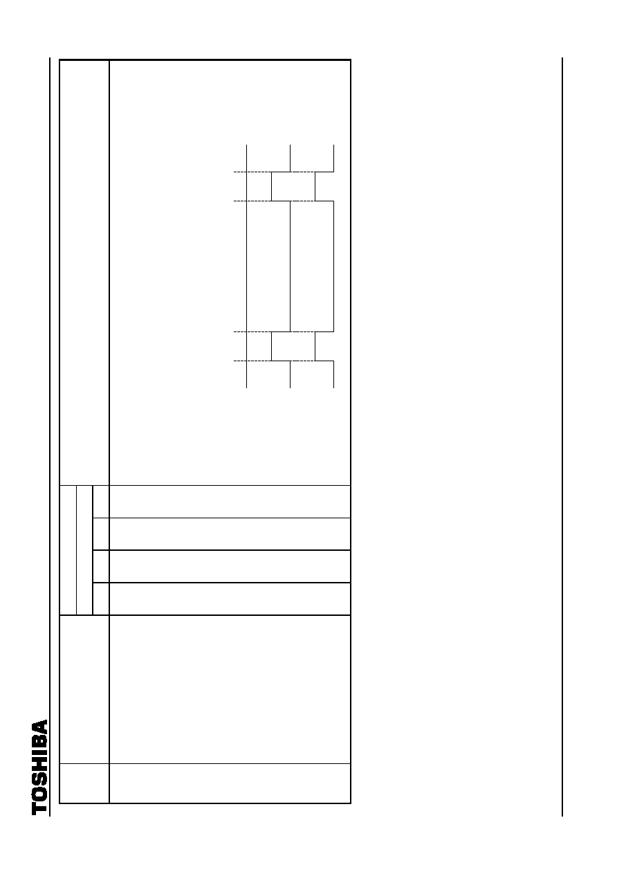
TA1316AN
2002-10-04
57
Test Conditions
SW mode
Note No.
Parameter
SW1
SW2
SW3
SW56
Test Method (test conditions: V
CC
= 9 V/2 V, Ta
= 25∞ ± 3∞C)
P05
Dynamic ABL detection voltage
B
A
C
OPEN (1) Set ABL GAIN to minimum (000), DYNAMIC ABL GAIN to maximum (111) and black stretch point 1 to off
(000).
(2) Connect external power supply (PS) to pin 53 and decrease voltage from 6.5 V.
(3) When DYNAMIC ABL POINT bus data is 000, 001, 110 and 100, repeat step (2) above. When pin 56 picture
period goes Low, measure PS voltages V
000
, V
001
, V
010
and V
100
.
(4) Determine voltage differential between V
000
and V
001
(V
001
), between V
000
and V
010
(
V
010
)
,
and between
V
000
and V
100
(
V
100
).
DV
***
= V
000
- V
001
(V
010
, V
100
)
Pin 2 waveform
Pin 56 detected
Pin 56 undetected
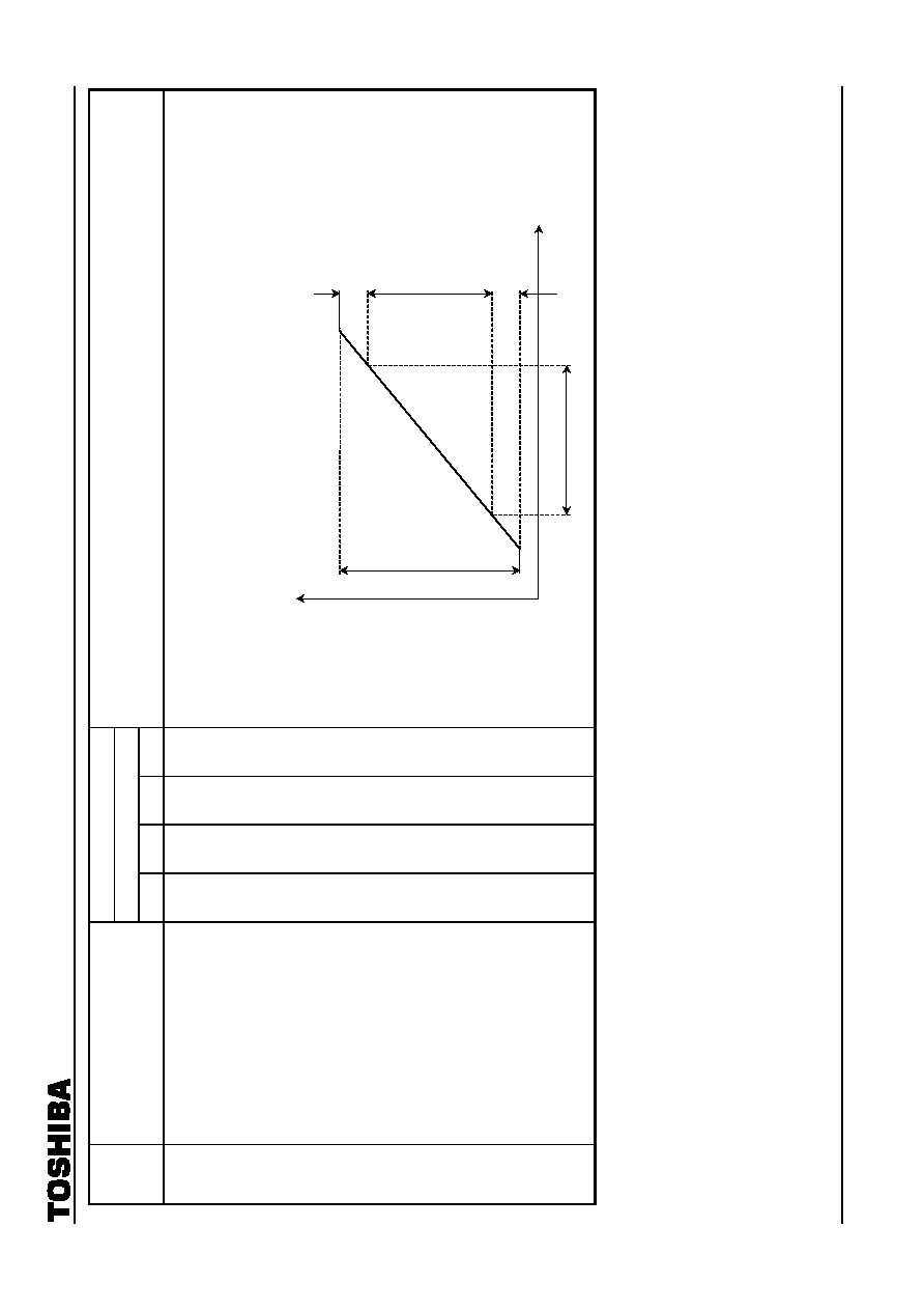
TA1316AN
2002-10-04
58
Test Conditions
SW mode
Note No.
Parameter
SW1
SW2
SW3
SW56
Test Method (test conditions: V
CC
= 9 V/2 V, Ta
= 25∞ ± 3∞C)
P06
Dynamic ABL sensitivity
B
A
C
ON
(1) Set black stretch point 1 to off (000) and connect external power supply (PS) to pin 53.
(2) When DYNAMIC ABL POINT is a minimum (000) and DYNAMIC ABL GAIN is a minimum (000) or a
maximum (111), plot pin 53 voltage characteristic in relation to pin 56 voltage.
(3) Determine gradients S
DAMIN
and S
DAMAX
using the graph below.
S
DAMIN
= Y/X S
DAMAX
= Y/X
Y
Pin 53
X
100%
10%
10%
Pin 56
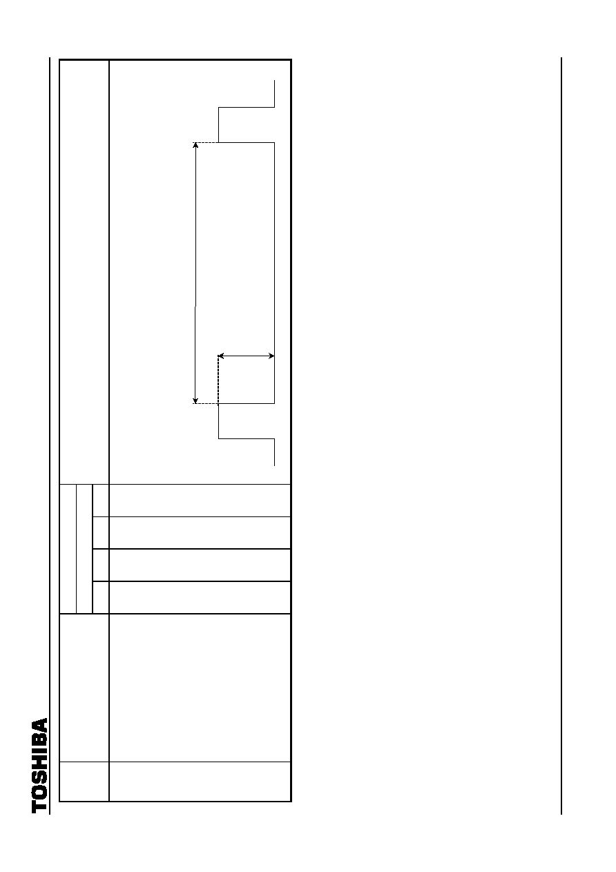
TA1316AN
2002-10-04
59
Test Conditions
SW mode
Note No.
Parameter
SW1
SW2
SW3
SW56
Test Method (test conditions: V
CC
= 9 V/2 V, Ta
= 25∞ ± 3∞C)
P07
Black level correction
B
A
C
OPEN (1) Set black stretch point 1 to off (000) and monitor pin 56.
(2) Set black level correction (BLC) to on (1), measure
V
1
(mV) and calculate BLC using the following formula.
(V
Z
: P09 value)
BLC
= [V
1
/(V
Z
◊ 10
3
)]
◊ 100 (IRE)
V
1
[mV]
Picture period
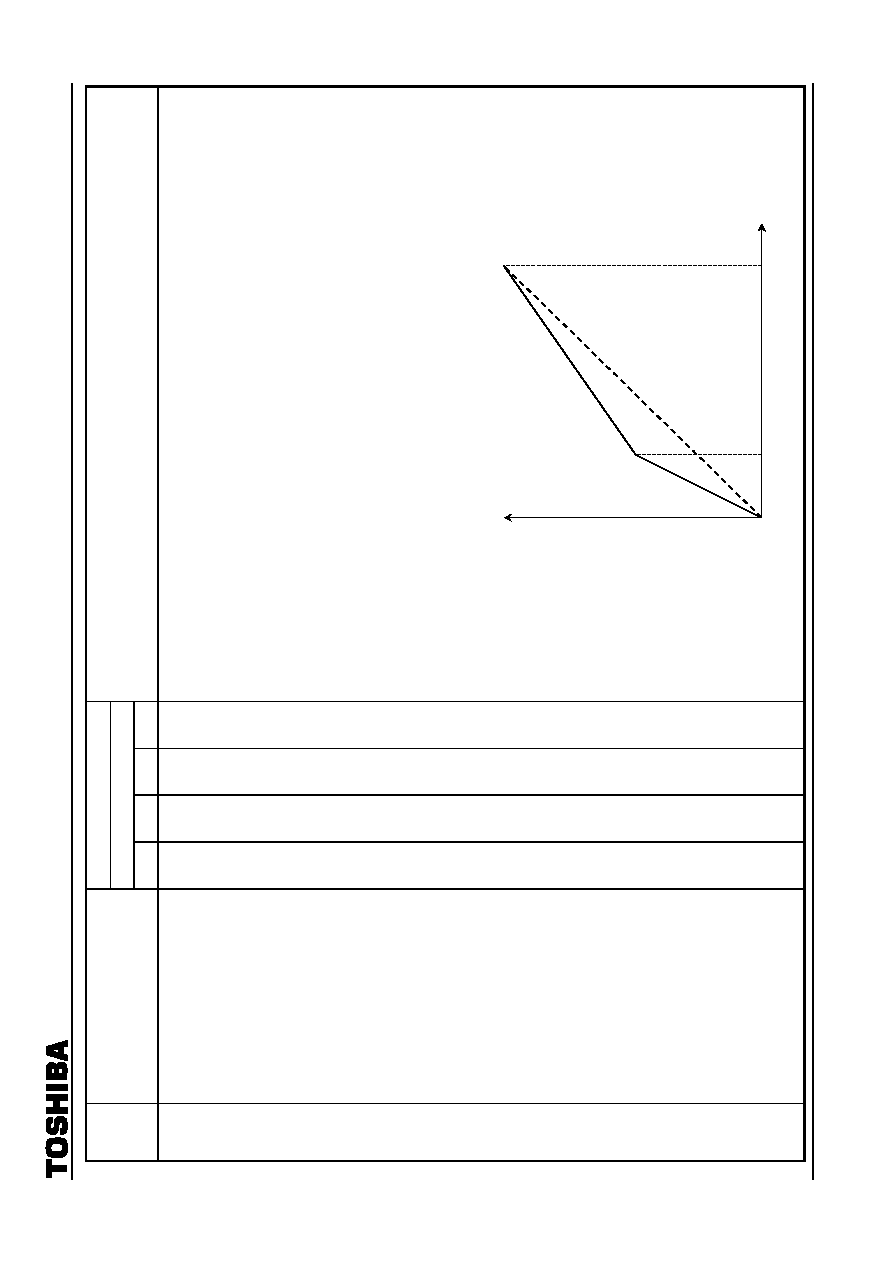
TA1316AN
2002-10-04
60
Test Conditions
SW mode
Note No.
Parameter
SW1
SW2
SW3
SW56
Test Method (test conditions: V
CC
= 9 V/2 V, Ta
= 25∞ ± 3∞C)
P08
Dynamic Y
correction point
A
B
A
OPEN (1)
Connect external power supply (PS1) to pin 3 and (PS2) to TP1. Set PS2 to 0 V.
(2) Set dynamic Y
point switch (DYNC-POINT) to 19 IRE (00), dynamic Y gain VS dark area (DYNC GAIN
VS DARK AREA) to off (000) and dynamic Y
dark area gain to off (00).
(3) When PS1 is increased from V
3
to V
3
+ 0.7 V, set V
3
to 0 V and plot voltage change in pin 56. (V
3
is pin
voltage of pin 3.)
(4) Set DYNC
GAIN VS DARK AREA to maximum (111), static Y dark area gain (STATIC-GAIN) to maximum
(11) and PS2 to 1 V.
(5) As in step (3) above, increase PS1 from V
3
to V
3
+ 0.7 V and plot pin 56 voltage change.
(6) Set DYNC
-POINT to 21 IRE (01), 25 IRE (10) and 30 IRE (11), increase PS1 from V
3
to V
3
+ 0.7 V and plot
pin 56 voltage change.
(7) Determine dynamic Y
point when DYNC-POINT is set to 19 IRE (00) as V
DGP00
using the graph below.
Also determine dynamic Y
point when DYNC-POINT is set to 21 IRE (01) as V
DGP01
; to 25 IRE (10) as
V
DGP10
; to 30 IRE (10) as V
DGP11
.
(8) Using V
DGP01
, V
DGP10
, and V
DGP11
thus determined, calculate P
DGP00
, P
DGP01
, P
DGP10
and P
DGP11
using the following formulae.
PDGP
00
= (V
DGP00
/0.7)
◊ 100
PDGPA
= PDGP
01
- PDGP
00
PDGP
01
= (V
DGP01
/0.7)
◊ 100
PDGPB
= PDGP
10
- PDGP
00
PDGP
10
= (V
DGP10
/0.7)
◊ 100
PDGPC
= PDGP
11
- PDGP
00
PDGP
11
= (V
DGP11
/0.7)
◊ 100
OFF
ON
Pin 56 voltage [V]
Pin 3 voltage
VDGP
***
100 IRE
TA1316AN
2002-10-04
61
Test Conditions
SW mode
Note No.
Parameter
SW1
SW2
SW3
SW56
Test Method (test conditions: V
CC
= 9 V/2 V, Ta
= 25∞ ± 3∞C)
P09
Dynamic Y
gain
A
B
A
OPEN (1) Connect external power supply (PS1) to pin 3 and (PS2) to TP1. Set PS2 to 0 V.
(2) Set DYNC
-POINT to 30 IRE (11), DYNC GAIN VS DARK AREA to off (000) and STATIC-GAIN to off (00).
(3) Set PS1 to V
3
and determine pin 56 voltage V
DGOFF1
.
(4) Set PS1 to V
3
+ 0.16 V and determine pin 56 voltage V
DGOFF2
.
(5) Set DYNC
GAIN VS DARK AREA to maximum (111), PS2 to 1 V and determine pin 56 voltage V
GDON
.
(6) Calculate G
DG
using the following formula.
G
DG
= 20 ◊ og (V
DGON
- V
DGOFF1
/V
DGOFF2
- V
DGOFF1
)
P10
Static Y
dark area gain
A
B
A
OPEN (1) Connect external power supply (PS1) to pin 3 and (PS2) to TP1. Set PS2 to 0 V.
(2) Set DYNC
-POINT to 30 IRE (11), DYNC GAIN VS DARK AREA to off (000) and STATIC-GAIN to off (00).
(3) Set PS1 to V
3
and determine pin 56 voltage V
SGOFF1
.
(4) Set PS1 to V
3
+ 0.16 V and determine pin 56 voltage V
SGOFF2
.
(5) Set STATIC
GAIN to maximum (11) and determine pin 56 voltage V
SGON
.
(6) Calculate G
SG
using the following formula.
G
SG
= 20 ◊ og (V
SGON
- V
SGOFF1
/V
SGOFF2
- V
SGOFF1
)
TA1316AN
2002-10-04
62
Test Conditions
SW mode
Note No.
Parameter
SW1
SW2
SW3
SW56
Test Method (test conditions: V
CC
= 9 V/2 V, Ta
= 25∞ ± 3∞C)
P11
DC restoration gain
B
B
C
ON
(1) Set picture mute to off (P-MODE: Normal1 (000)), DC restoration start point to minimum (000) and DC
restoration limit point (DC REST LIMIT) to 100% (11) and connect external power supply PS1 to pin 3.
(2) Measure DC level of pin 43 picture period. When use PS1 at V
3
as reference, Set PS1 to V
3
+ 0.7 V and
adjust DC level to 0.7 V using UNI-COLOR.
(3) Set DC REST RATE to minimum (000) and measure V
DT1
and V
DT2
when pin 3 is at V
3
and at V
3
+ 0.1 V
(see figure below).
(4) Measure V
DT3
when pin 3 is at V
3
+ 0.1 V. Set DC REST RATE to maximum (111) and measure V
DT3
.
(5) Set DC restoration rate switch (DCRR-SW) to 100% or less (1) and pin 3 to V
3
+ 0.1 V, and measure V
DT4
.
Set DC REST RATE to maximum (111) and measure V
DT4
.
(6) Calculate ADT
100
, ADT
135
and ADT
65
using the following formulae.
ADT
100
= (V
DT2
[V]
- V
DT1
[V])
˜ 0.1 [V]
ADT
135
= (V
DT3
[V]
- V
DT1
[V])
˜ 0.1 [V]
ADT
65
= 1 - {(V
DT2
[V]
- V
DT4
[V])
˜ 0.1 [V]}
Picture period
V
DT1
V
3
[V]
V
DT2
V
DT3
V
DT4
V
3
+ 0.1 V
Pin 43 waveform
TA1316AN
2002-10-04
63
Test Conditions
SW mode
Note No.
Parameter
SW1
SW2
SW3
SW56
Test Method (test conditions: V
CC
= 9 V/2 V, Ta
= 25∞ ± 3∞C)
P12
DC restoration start point
B
B
C
ON
(1) Set picture mute to off (P-MODE: Normal1 (000)), DC restoration start point to minimum (000) and DC REST
LIMIT to 100% (11), and connect external power supply PS1 to pin 3.
(2) Measure DC level of pin 43 picture period. Use PS1 at V
3
as reference. When PS1 is set to V
3
+ 0.7 V, adjust
DC level to
+1.0 V using UNI-COLOR.
(3) Set DC REST RATE to minimum (000), increase PS1 from V
3
and plot voltage relationship between pin 56
(DC voltage) and pin 43 (picture period voltage).
(4) Set DC REST RATE to maximum (111), increase PS1 from V
3
and plot voltage relationship between pins 56
and 43.
(5) Set DC REST RATE to maximum (111), DC restoration start point to maximum (111), increase PS1 from V
3
and plot voltage relationship between pins 56 and 43.
(6) Calculate V
DT0
and V
DT1
using the following formulae.
V
DT0
= [(V
SP0
- V
56
)/1 V]
◊ 100%
V
DT1
= [(V
SP1
- V
56
)/1 V]
◊ 100%
DC restoration rate: 000
DC restoration start point: 111
DC restoration start point: 000
Pin 56
V
SP1
V
SP0
V
PC
Pin 43
TA1316AN
2002-10-04
64
Test Conditions
SW mode
Note No.
Parameter
SW1
SW2
SW3
SW56
Test Method (test conditions: V
CC
= 9 V/2 V, Ta
= 25∞ ± 3∞C)
P13
DC restoration limit point
B
B
C
ON
(1) Set picture mute to off (P-MODE: Normal1 (000)), UNI-COLOR to maximum (1111111) and DC restoration
start point to minimum (000), and connect external power supply PS to pin 56.
(2) Set DC REST RATE to maximum (111).
(3) Increase PS from 5 V, monitor pin 43 and plot DC restoration.
(4) Change DC REST LIMIT and repeat step (3) above. Determine V
L11
, V
L10
, V
L01
and V
L00
using the graph
below. Calculate P
DTL11
, P
DTL10
, P
DTL01
and P
DTL00
using the following formulae.
P
DTL11
= [(V
L11
- V
56
)/1.0]
◊ 100%
P
DTL10
= [(V
L10
- V
56
)/1.0]
◊ 100%
P
DTL01
= [(V
L01
- V
56
)/1.0]
◊ 100%
P
DTL00
= [(V
L00
- V
56
)/1.0]
◊ 100%
100% (00)
87% (01)
73% (10)
60% (11)
V
L01
V
L00
V
L10
V
L11
Pin 56
Pin 43

TA1316AN
2002-10-04
65
Test Conditions
SW mode
Note No.
Parameter
SW1
SW2
SW3
SW56
Test Method (test conditions: V
CC
= 9 V/2 V, Ta
= 25∞ ± 3∞C)
P14
Sharpness control range
B
B
A
ON
(1) Input sine wave (frequency variable) to TPA.
(2) Set pin 3 amplitude to 20 mV
P-P
.
(3) Set UNI-COLOR to maximum (1111111), SHR-TRACKING to SRT-GAIN minimum (11), APACON peak
frequency (APACON PEAK f
0
) to 15 M (00) and color detail enhancer (CDE) to center (10).
(4) Set picture mute to off (P-MODE: Normal1 (000)) and monitor pin 43.
(5) Set picture sharpness (PICTURE-SHARPNESS) to center (1000000) and measure amplitude V
100
when
input frequency is 100 kHz.
(6) Set PICTURE-SHARPNESS to maximum (1111111) and measure amplitude V
MAX00
when input frequency is
F
AP00
. Calculate G
MAX00
using the following formula.
(7) Set PICTURE-SHARPNESS to minimum (0000000) and measure amplitude V
MIN00
when input frequency is
F
AP00
. Calculate G
MIN00
using the following formula.
(8) Set APACON PEAK f
0
to 8.8 M (01) and measure amplitudes V
MAX01
and V
MIN01
as in steps (6) and (7)
when input frequency is F
AP01
. Calculate G
MAX01
and G
MIN01
using the following formulae.
(9) Set APACON PEAK f
0
to 7.5 M (10) and measure amplitudes V
MAX10
and V
MIN10
as in steps (6) and (7)
when input frequency is F
AP10
. Calculate G
MAX10
and G
MIN10
using the following formulae.
(10) Set APACON PEAK f
0
to 5 M (11) and measure amplitudes V
MAX11
and V
MIN11
as in steps (6) and (7) when
input frequency is F
AP11
. Calculate G
MAX11
and G
MIN11
using the following formulae.
G
MAX
***
= 20 ◊ og (V
MAX
***
˜ V
100
) [dB]
G
MIN
***
= 20 ◊ og (V
MIN
***
˜ V
100
) [dB]
*: When using a spectrum analyzer for monitoring, measure gain for low frequency.
TA1316AN
2002-10-04
66
Test Conditions
SW mode
Note No.
Parameter
SW1
SW2
SW3
SW56
Test Method (test conditions: V
CC
= 9 V/2 V, Ta
= 25∞ ± 3∞C)
P15
Sharpness control center
characteristic
B
B
A
ON
(1) Input sine wave (frequency variable) to TPA.
(2) Set pin 3 amplitude to 20 mV
P-P
.
(3) Set UNI-COLOR to maximum (1111111), SHR-TRACKING to SRT-GAIN minimum (11), APACON peak
frequency (APACON PEAK f
0
) to 15 M (00) and color detail enhancer (CDE) to center (10).
(4) Set picture mute to off (P-MODE: Normal1 (000)) and monitor pin 43.
(5) Set PICTURE-SHARPNESS to center (1000000) and measure amplitude V
100
when input frequency is 100
kHz.
(6) Measure pin 43 amplitude V
CEN00
when input frequency is F
AP00
with PICTURE-SHARPNESS set to center
(1000000). Calculate G
CEN00
using the following formula.
(7) Set APACON PEAK f
0
to 8.8 M (01) and measure amplitude V
CEN01
as in step (6) when input frequency is
F
AP01
. Calculate G
CEN01
using the following formula.
(8) Set APACON PEAK f
0
to 7.5 M (10) and measure amplitude V
CEN10
as in step (6) when input frequency is
F
AP10
. Calculate G
CEN10
using the following formula.
(9) Set APACON PEAK f
0
to 5 M (11) and measure amplitudes V
CEN11
as in step (6) when input frequency is
F
AP11
. Calculate G
CEN11
using the following formula.
G
CEN
***
= 20 ◊ og (V
CEN
***
˜ V
100
) [dB]
*: When using a spectrum analyzer for monitoring, measure gain for low frequency.
TA1316AN
2002-10-04
67
Test Conditions
SW mode
Note No.
Parameter
SW1
SW2
SW3
SW56
Test Method (test conditions: V
CC
= 9 V/2 V, Ta
= 25∞ ± 3∞C)
P16
YNR characteristic
B
B
A
ON
(1) Input sine wave (frequency variable) to TPA.
(2) Set pin 3 amplitude to 20 mV
P-P
.
(3) Set UNI-COLOR to maximum (1111111), SHR-TRACKING to SRT-GAIN minimum (11), APACON peak
frequency (APACON PEAK f
0
) to 15 M (00) and color detail enhancer (CDE) to center (10).
(4) Set picture mute to off (P-MODE: Normal1 (000)) and monitor pin 43.
(5) Set PICTURE-SHARPNESS to center (1000000) and measure amplitude V
100
when input frequency is 100
kHz.
(6) Set YNR to on (1) and PICTURE-SHARPNESS to minimum (0000000). Measure pin 43 amplitude V
TRAP00
when input frequency is F
AP00
and calculate G
YNRT00
using the following formula.
(7) When PICTURE-SHARPNESS is set to 0000011 and measure pin 43 amplitude V
FLAT00
. Calculate
G
YNRF00
using the following formula.
(8) Set APACON PEAK f
0
to 8.8 M (01) and measure amplitude V
TRAP01
as in step (7) when input frequency is
F
AP01
. Calculate G
TRAP01
using the following formula.
(9) Set APACON PEAK f
0
to 7.5 M (10) and measure amplitude V
TRAP10
as in step (7) when input frequency is
F
AP10
. Calculate G
TRAP10
using the following formula.
(10) Set APACON PEAK f
0
to 5 M (11) and measure amplitude V
TRAP11
as in step (7) when input frequency is
F
AP11
. Calculate G
TRAP11
using the following formula.
G
YNRT
**
= 20 ◊ og (V
TRAP
**
/V
100
)
[dB]
G
YNRF
**
= 20 ◊ og (V
FLAT
**
/V
100
)
[dB]
*: When using a spectrum analyzer for monitoring, measure gain for low frequency.
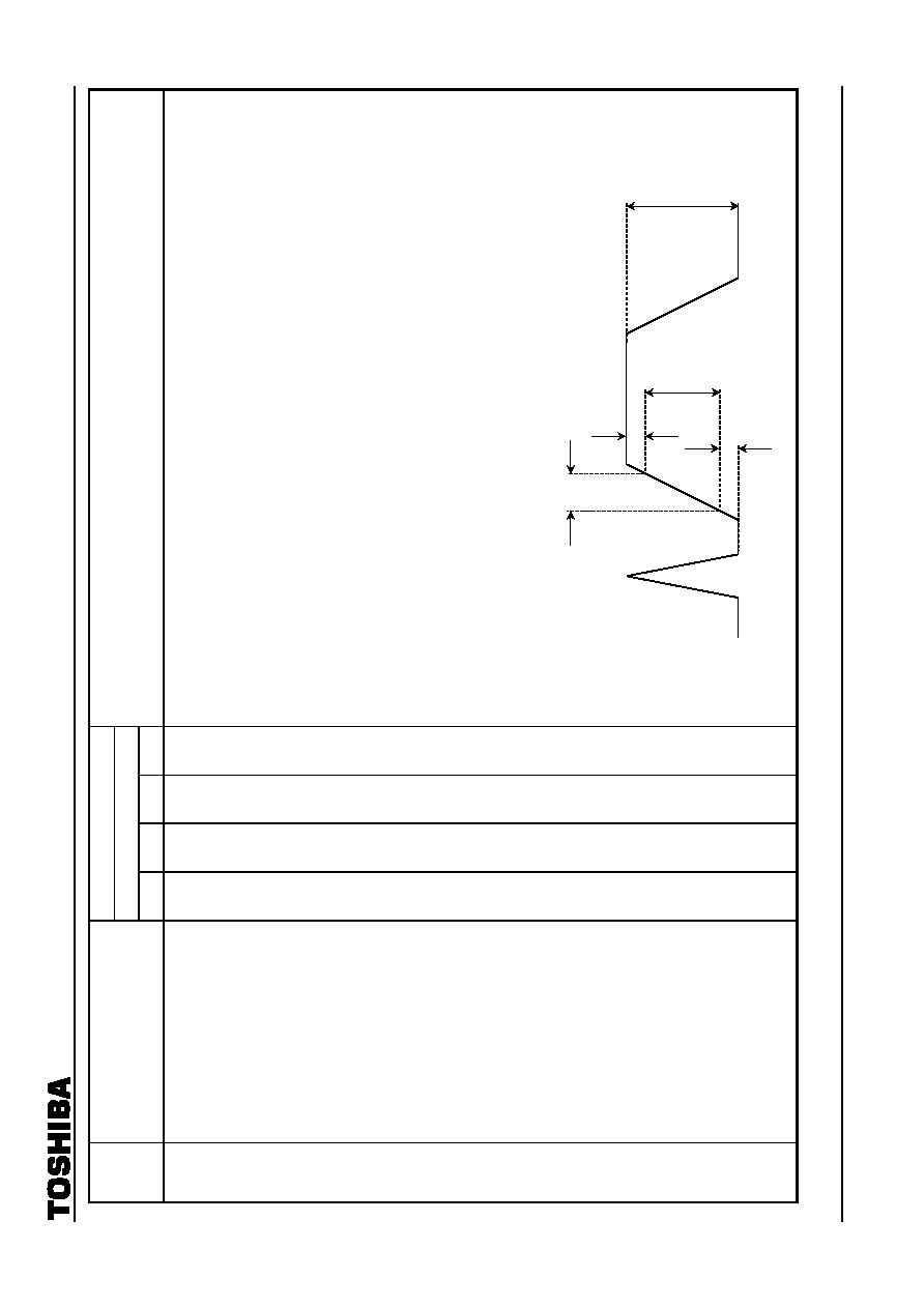
TA1316AN
2002-10-04
68
Test Conditions
SW mode
Note No.
Parameter
SW1
SW2
SW3
SW56
Test Method (test conditions: V
CC
= 9 V/2 V, Ta
= 25∞ ± 3∞C)
P17
Control of SRT response to 2T pulse
input
B
B
A
ON
(1) Input 2T pulse (0.7 V
P-P
) signal to TPA and set picture mute to off (P-MODE: Normal1 (000)), UNI-COLOR to
maximum (1111111), and SHR-TRACKING to SRT-GAIN minimum (11), CDE to center (10) and
PICTURE-SHARPNESS to center (1000000).
(2) Set APACON frequency to 15 M (00) and monitor pin 43.
(3) Measure T
SRTMIN00
and V
SRTMIN00
as shown in the figure below.
(4) Set SHR-TRACKING to SRT-GAIN maximum (00) and measure T
SRTMAX00
and V
SRTMAX00
.
(5) Set APACON frequency to 8.8 M (01), SHR-TRACKING to SRT-GAIN minimum (11) and maximum (00) as in
step (4) above, and measure T
SRTMIN01
, V
SRTMIN01
, T
SRTMAX01
and V
SRTMAX01
.
(6) Set APACON frequency to 7.5 M (10), SHR-TRACKING to SRT-GAIN minimum (11) and maximum (00) as in
step (4) above, and measure T
SRTMIN10
, V
SRTMIN10
, T
SRTMAX10
and V
SRTMAX10
.
(7) Set APACON frequency to 5 M (11), SHR-TRACKING to SRT-GAIN minimum (11) and maximum (00) as in
step (4) above, and measure T
SRTMIN11
, V
SRTMIN11
, T
SRTMAX11
and V
SRTMAX11
.
(8) Calculate using the following formulae.
T
SRT00
= 20 ◊ og [((V
SRTMAX00
/T
SRTMAX00
)/(V
SRTMIN00
/T
SRTMIN00
)]
T
SRT01
= 20 ◊ og [(V
SRTMAX01
/T
SRTMAX01
)/(V
SRTMIN01
/T
SRTMIN01
)]
T
SRT10
= 20 ◊ og [(V
SRTMAX10
/T
SRTMAX10
)/(V
SRTMIN10
/T
SRTMIN10
)]
T
SRT11
= 20 ◊ og [(V
SRTMAX11
/T
SRTMAX11
)/(V
SRTMIN11
/T
SRTMIN11
)]
20%
100%
T
***
20%
V
***

TA1316AN
2002-10-04
69
Test Conditions
SW mode
Note No.
Parameter
SW1
SW2
SW3
SW56
Test Method (test conditions: V
CC
= 9 V/2 V, Ta
= 25∞ ± 3∞C)
P18
VSM gain
B
B
A
ON
(1) Input sine wave of frequency F
VSM2
to TPA.
(2) Set picture mute to off (P-MODE: Normal1 (000)), and pin 3 amplitude to 0.02 V
P-P
.
(3) Vary VSM GAIN from off (000) to maximum (111) and measure pin 54 amplitudes V
001
, V
010
, V
011
, V
100
,
V
101
, V
110
and V
111
. Set input amplitude to 0.7 V
P-P
and measure pin 54 amplitude V
000
when VSM GAIN is
OFF (000).
(4) Calculate using the following formulae.
G
V000
= 20
◊ og (V
000
/0.7) [dB]
G
V001
= 20
◊ og (V
001
/0.02) [dB]
G
V010
= 20
◊ og (V
010
/0.02) [dB]
G
V011
= 20
◊ og (V
011
/0.02) [dB]
G
V100
= 20
◊ og (V
100
/0.02) [dB]
G
V101
= 20
◊ og (V
101
/0.02) [dB]
G
V110
= 20
◊ og (V
110
/0.02) [dB]
G
V111
= 20
◊ og (V
111
/0.02) [dB]
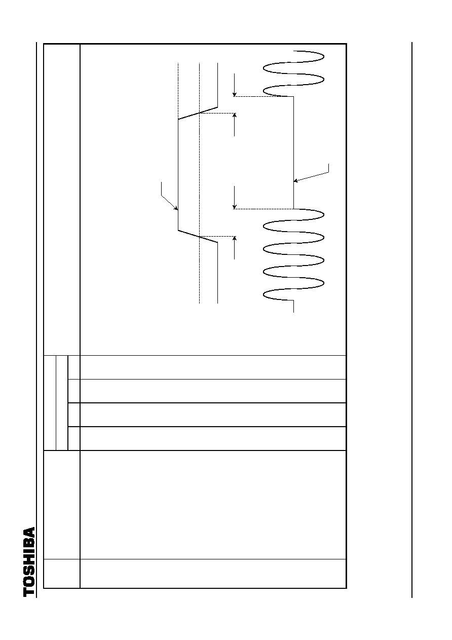
TA1316AN
2002-10-04
70
Test Conditions
SW mode
Note No.
Parameter
SW1
SW2
SW3
SW56
Test Method (test conditions: V
CC
= 9 V/2 V, Ta
= 25∞ ± 3∞C)
P19
Response time for VSM fast muting
B
B
A
ON
(1) Input sine wave of frequency F
VSM
to TPA.
(2) Set picture mute to off (P-MODE: Normal1 (000)), VSM GAIN to 100 and pin 3 amplitude to 0.1 V
P-P
. Monitor
pin 54.
(3) Input pulse as shown below to pin 49 and determine response times T
VM49A
and T
VM49B
.
(4) Likewise input pulse to pin 50 and determine response times T
VM50A
and T
VM50B
.
(5) Likewise input pulse to pin 51 and determine response times T
VM51A
and T
VM51B
.
Square wave (50 kHz, 2 V
P-P
)
Pin 54
waveform
T
VM49A
T
VM49B
0 V
2 V
Pin 49
waveform
V
SR49
[V]
Mute period

TA1316AN
2002-10-04
71
Test Conditions
SW mode
Note No.
Parameter
SW1
SW2
SW3
SW56
Test Method (test conditions: V
CC
= 9 V/2 V, Ta
= 25∞ ± 3∞C)
P20
VSM limit
B
B
A
ON
(1) Input sine wave of frequency F
VSM2
to TPA.
(2) Set picture mute to off (P-MODE: Normal1 (000)), VSM GAIN to 111 and pin 3 amplitude to 0.7 V
P-P
.
(3) Measure pin 54 amplitudes V
LU
and V
LD
[V
P-P
] as shown below.
V
LU
V
LD
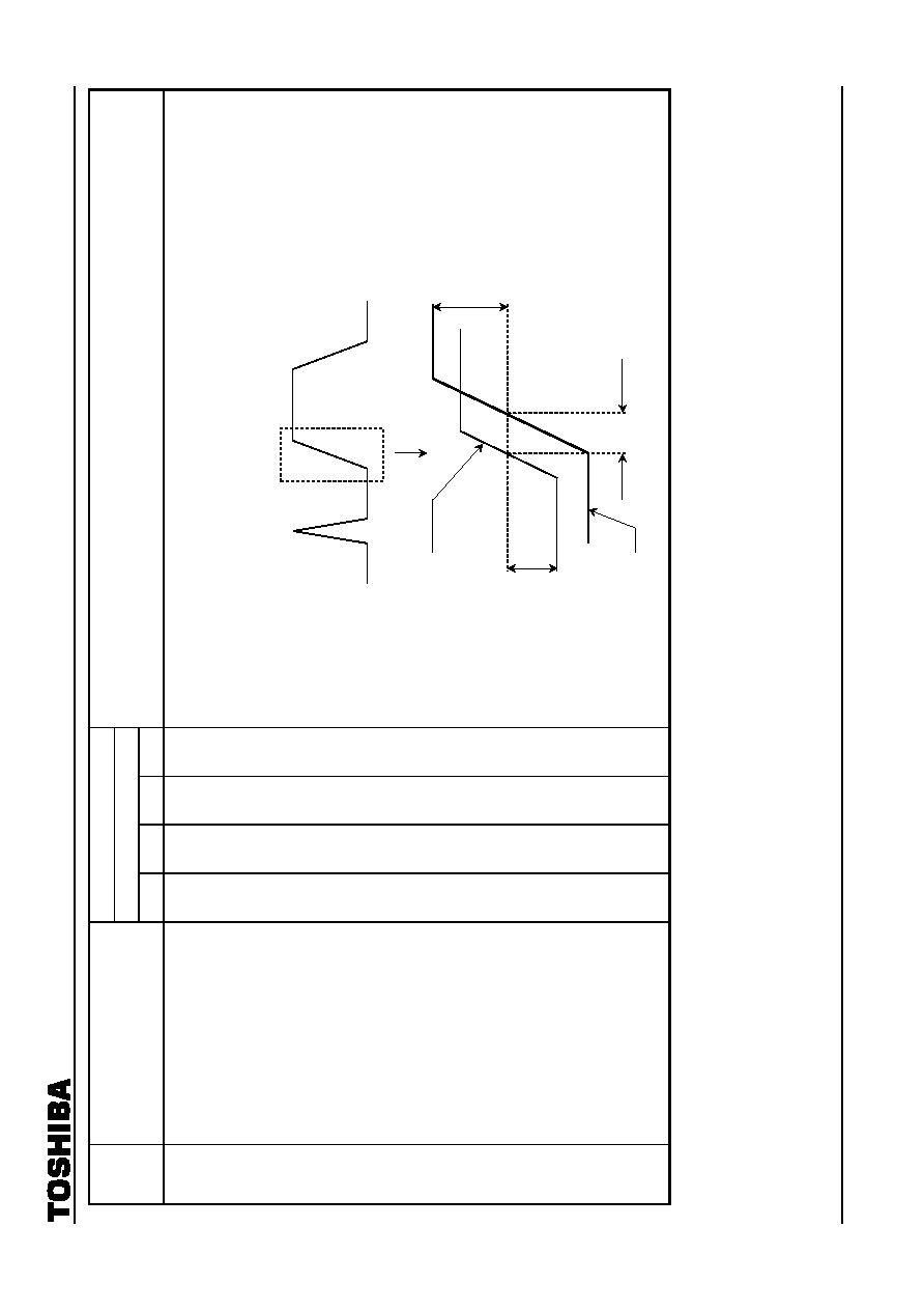
TA1316AN
2002-10-04
72
Test Conditions
SW mode
Note No.
Parameter
SW1
SW2
SW3
SW56
Test Method (test conditions: V
CC
= 9 V/2 V, Ta
= 25∞ ± 3∞C)
P21
Delay time from Y input to R output
B
B
A
ON
(1)
Set picture mute to off (P-MODE: Normal1 (000)), UNI-COLOR to maximum (1111111), SHR-TRACKING to
SRT-GAIN minimum (11) and input 2T pulse signal (STD) to TPA.
(2) Set PICTURE-SHARPNESS to center (1000000).
(3) Determine T
YR
by monitioring pins 43 and 3 as shown below.
2T pulse (STD)
50%
50%
T
YR
Pin 43
Pin 3
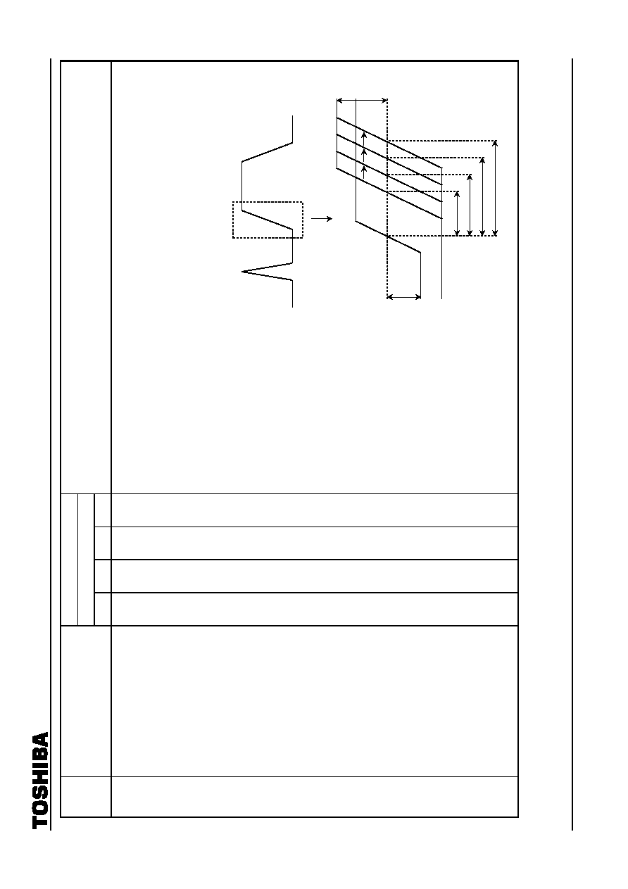
TA1316AN
2002-10-04
73
Test Conditions
SW mode
Note No.
Parameter
SW1
SW2
SW3
SW56
Test Method (test conditions: V
CC
= 9 V/2 V, Ta
= 25∞ ± 3∞C)
P22
Y delay time change
B
B
A
ON
(1)
Set picture mute to off (P-MODE: Normal1, 000), UNI-COLOR to maximum (1111111) and SHR-TRACKING
to SRT-GAIN minimum (11), and input T2 pulse signal (approx. 0.7 Vp-p) to TPA.
(2) Set picture sharpness to center (1000000).
(3) Monitor pin 3 and pin 43, and determine the time difference YDL00 for each signal at the 50% point as shown
below.
(4) Set Y/C-DL1 to
+5 ns (1) and determine YDL01.
(5) Set Y/C-DL1 to
+0 ns (0) and Y/C-DL2 to +10 ns (1), and determine YDL10.
(6) Set Y/C-DL1 to
+5 ns (1) and Y/C-DL2 to +10 ns (1), and determine YDL11.
(7) Determine YDLA, YDLB and YDLC as follows:
YDLA
= YDL01 - YDL00
YDLB
= YDL10 - YDL00
YDLC
= YDL11 - YDL00
T2 pulse signal
approx. 0.7 Vp-p
50%
50%
YDL00
#3
#43
YDL01
YDL10
YDL11
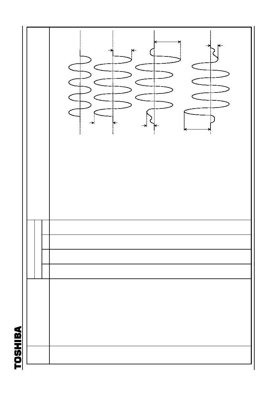
TA1316AN
2002-10-04
74
Test Conditions
SW mode
Note No.
Parameter
SW1
SW2
SW3
SW56
Test Method (test conditions: V
CC
= 9 V/2 V, Ta
= 25∞ ± 3∞C)
P23
Transfer distortion correction
B
B
A
ON
(1) Input multi-burst signal (frequency equivalent to 4.2 MHz) of signal A to TPA. Set picture mute to off
(P-MODE: Normal1 (000)), UNI-COLOR to maximum (1111111), SHR-TRACKING to SRT-GAIN minimum
(11) and CDE to minimum (00).
(2) Set PICTURE-SHARPNESS to
flat (near DEC[24]), APACON
PEAK f
0
to 5 M (11) and monitor
pin 43.
(3) Input sine wave signal A (approx.
4.2 MHz) becomes signal B on
pin 43 as shown at right.
Determine S
A
and S
B
.
(4) When Y-GROUP DELAY
CORRECTION is set to minimum
(0000), signal A becomes signal
C on pin 43. Determine S
AMIN
and S
BMIN
.
(5) When Y-GROUP DELAY
CORRECTION is set to
maximum (1111), signal A
becomes signal D on pin 43.
Determine S
AMAX
and S
BMAX
.
(6) Calculate using the following formulae.
G
AMIN
= 20 ◊ og (S
AMIN
/S
A
) [dB]
G
BMIN
= 20 ◊ og (S
BMIN
/S
B
) [dB]
G
AMAX
= 20 ◊ og (S
AMAX
/S
A
) [dB]
G
BMAX
= 20 ◊ og (S
BMAX
/S
B
) [dB]
Note: The input sine wave starts and ends within the picture period. It is like a burst signal, not a continuous wave.
Signal
A
Signal
B
Signal
C
Signal
D
S
A
S
B
S
AMIN
S
BMIN
S
AMAX
S
AMAX
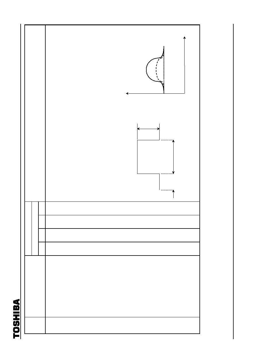
TA1316AN
2002-10-04
75
Test Conditions
SW mode
Note No.
Parameter
SW1
SW2
SW3
SW56
Test Method (test conditions: V
CC
= 9 V/2 V, Ta
= 25∞ ± 3∞C)
P24
Color detail enhancer
B
B
A
ON
(1) Set picture mute to off (P-MODE: Normal1 (000)), UNI-COLOR to maximum (1111111), SHR-TRACKING to
SRT-GAIN minimum (11), COLOR to center (1000000), color limiter level (CLT) to 2 Vp (1) and C-SRT-FREQ
to 4.5 M (10). Input SWEEP signal to TPA and set pin 3 amplitude to 20 mV
P-P
. Set SW4 to A. Input signal
(pin 4 amplitude: 0.2 V
P-P
) to TP4 as shown in the figure below.
(2) Set PICTURE-SHARPNESS to center (1000000) and Y DETAIL CONTROL to center (10000), and monitor
pin 41 using a spectrum analyzer.
(3) Set low-frequency area to 0dB when CDE is set to minimum (00) and measure peak level G
CDEMIN
.
(4) Set low-frequency area to 0dB when CDE is set to maximum (11) and measure peak level G
CDEMAX
.
(5) Calculate using the following formula.
G
CDE00
= G
CDEMAX00
- G
CDEMIN00
(6) Set APACON PEAK f
0
to 15 M (00), 8.8 M (01), 7.5 M (10) and 5 M (11), and measure peak levels G
CDE00
,
G
CDE01
, G
CDE10
and G
CDE11
.
max
Output gain [dB]
Input frequency [MHz]
0 dB
Picture period
BLK period
0.2 V
p-p
min
TA1316AN
2002-10-04
76
Test Conditions
SW mode
Note No.
Parameter
SW1
SW2
SW3
SW56
Test Method (test conditions: V
CC
= 9 V/2 V, Ta
= 25∞ ± 3∞C)
P25
Y detail control range
B
B
A
ON
(1) Set picture mute to off (P-MODE: Normal1 (000)), UNI-COLOR to maximum (1111111), SHR-TRACKING to
SRT-GAIN minimum (11) and CDE to center (10). Input SWEEP signal to TPA.
(2) Set pin 3 amplitude to 20 mV
P-P
.
(3) Set PICTURE-SHARPNESS to minimum (0000000) and Y DETAIL CONTROL to maximum (11111), and
monitor pin 43 using a spectrum analyzer.
(4) Set low-frequency area to 0dB. Set APACON PEAK f
0
to 15 M (00), 8.8 M (01), 7.5 M (10) and 5 M (11), and
measure peak levels G
YDMAX00
, G
YDMAX01
, G
YNMAX10
and G
YDMAX11
.
(5) Set Y DETAIL CONTROL to center (10000) and measure peak levels G
YDCEN00
, G
YDCEN01
, G
YDCEN10
and
G
YDCEN11
.
(6) Set Y DETAIL CONTROL to minimum (00000) and measure peak levels G
YDMIN00
, G
YDMIN01
, G
YNDIN10
and G
YDMIN11
.
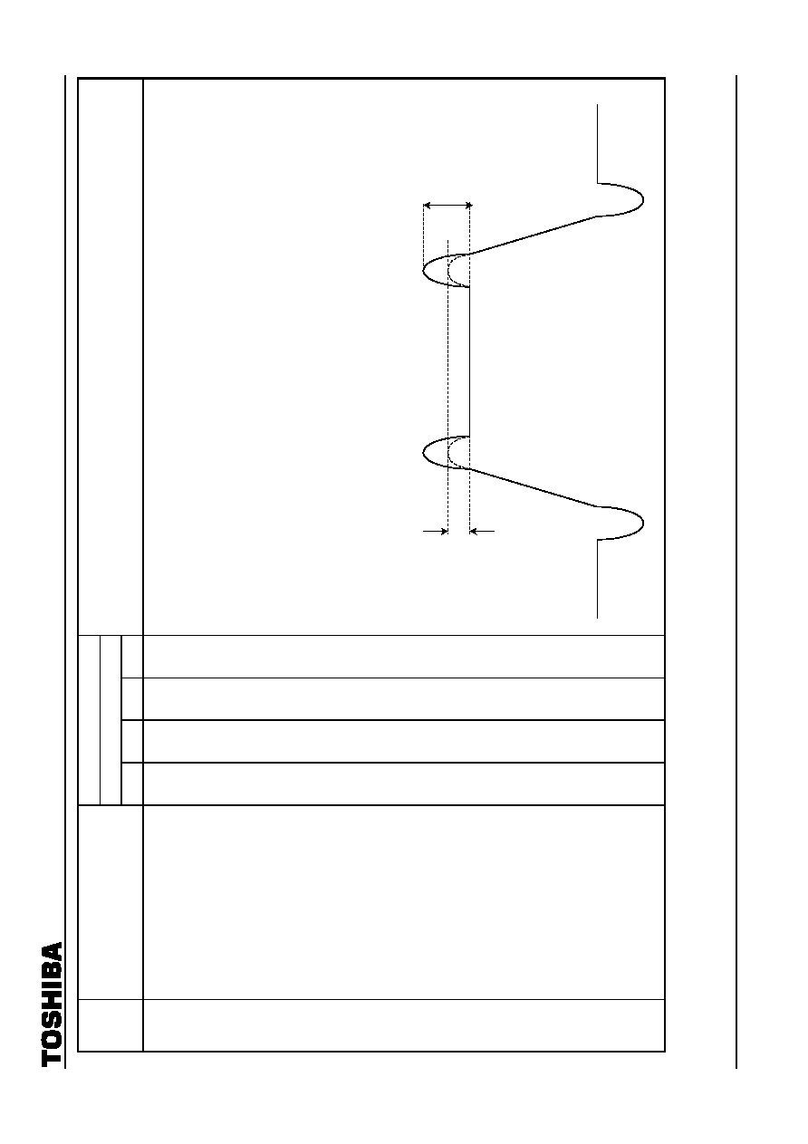
TA1316AN
2002-10-04
77
Test Conditions
SW mode
Note No.
Parameter
SW1
SW2
SW3
SW56
Test Method (test conditions: V
CC
= 9 V/2 V, Ta
= 25∞ ± 3∞C)
P26
APACON white peak limiter
B
B
A
ON
(1) Set picture mute to off (P-MODE: Normal1 (000)), UNI-COLOR to 1101000, SHR-TRACKING to SRT-GAIN
maximum (00) and CDE to maximum (11). Input T pulse signal (0.7 V
P-P
) to TPA.
(2) Set PICTURE-SHARPNESS to maximum (111111) and APACON PEAK f
0
to 5 M (11), and monitor pin 43.
(3) When APACON white peak limiter is off (000), measure positive spike amplitude V
WPLOFF1
.
(4) When APACON white peak limiter is at maximum (111), measure positive spike amplitude V
WPLMAX1
.
(5) Set UNI-COLOR to center (1000000). When APACON white peak limiter is off (000) and at maximum (111),
measure positive spike amplitudes V
WPLOFF2
and V
WPLMAX2
.
(6) Set UNI-COLOR to minimum (0000000). When APACON white peak limiter is off (000) and at maximum
(111), measure positive spike amplitudes V
WPLOFF3
and V
WPLMAX3
.
(7) Calculate using the following formulae.
G
WPL1
= 20 ◊ og (V
WPLMAX1
/V
WPLOFF1
) [dB]
G
WPL2
= 20 ◊ og (V
WPLMAX2
/V
WPLOFF2
) [dB]
G
WPL3
= 20 ◊ og (V
WPLMAX3
/V
WPLOFF3
) [dB]
V
WPLOFF
V
WPLMAX
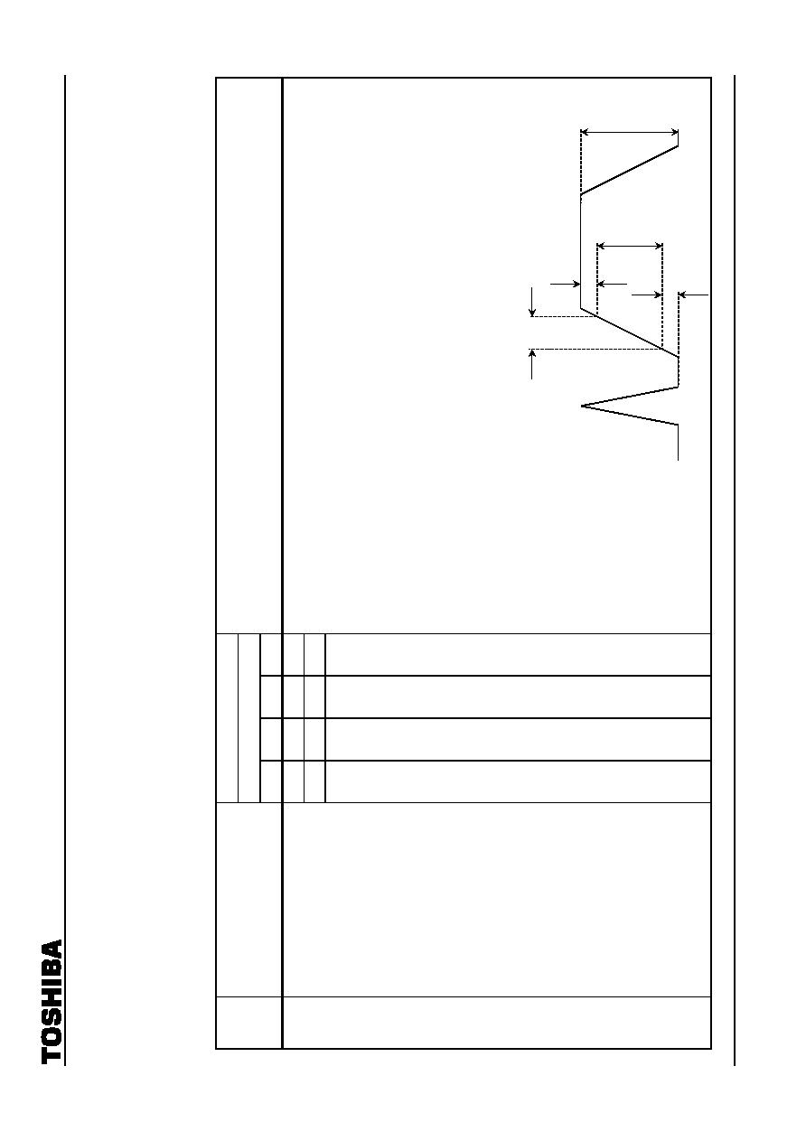
TA1316AN
2002-10-04
78
Test Conditions for Color Difference Signal 1/YUV Input and Matrix
Common Test Conditions for Color Difference Signal 1/YUV Input and Matrix
(1) SW1
= B, SW2 = B, SW20 = ON, SW33SW39 = A, SW54 = OPEN, SW56 = OPEN
(2) Send BUS control data with preset values.
(3) Set ACB MODE to off (0) and high bright color (HI BRT) to off (0).
(4) Input sync signal [signal in sync with input signal for testing, except for SWEEP signal] to pin 14 (SYNC IN) and set SYNC-INPUT to (10).
Test Conditions
SW mode
Note No.
Parameter
SW3
SW4
SW5
SW7
Test Method (test conditions: V
CC
= 9 V/2 V, Ta = 25∞ ± 3∞C)
C
A
A
OPEN
SW8
SW9
SW10
S01
Color SRT gain
B
B
B
(1) Set Y mute to on (P-MODE: Y-MUTE (001)), YUV INPUT MODE to Through (10), BRIGHTNESS to center
(10000000), COLOR to center (1000000) and UNI-COLOR to maximum (1111111).
(2) Input 2T pulse signal to TP4 and set pin 4 amplitude to 350 mV
P-P
.
(3) Monitor pin 41 output waveform. When C-SRT-FREQ is 5 MHz (00), measure edge gradients SB00MIN,
SB00CEN and SB00MAX when COLOR SRT GAIN is at minimum (000), center (100) and maximum (111) as
in shown in the figure below. Set SB00MIN to 0 dB, determine GS
B00CEN
= 20 ◊ og (SB00CEN/SB00MIN)
and GS
B00MAX
= 20 ◊ og (SB00MAX/SB00MIN).
(4) Repeat step (3) above, setting C-SRT-FREQ to 6.7 MHz (01) and 10 MHz (10), and measure edge gradients
when COLOR SRT GAIN is at minimum (000), center (100) and maximum (111). Determine GS
B01CEN
,
GS
B10CEN
, GS
B01MAX
and GS
B10MAX
.
(5) Input 2T pulse signal to TP5 and set pin 5 amplitude to 350 mV
P-P
.
(6) Monitor pin 43 output waveform. When C-SRT-FREQ is 5 MHz (00), measure edge gradients SR00MIN,
SR00CEN and SR00MAX when COLOR SRT GAIN is at minimum (000), center (100) and maximum (111) as
shown in the figure below. Set SR00MIN to 0dB, determine GS
R00CEN
= 20 ◊ og (SR00CEN/SR00MIN)
and GS
R00MAX
= 20 ◊ og (SR00MAX/SR00MIN).
(7) Repeat step (3) above,
setting C-SRT-FREQ to
6.7 MHz (01) and 10
MHz (10), and measure
edge gradients when
COLOR SRT GAIN is at
minimum (000), center
(100) and maximum
(111). Determine
GS
R01CEN
, GS
R10CEN
,
GS
R01MAX
and
GS
R10MAX
.
10%
100%
T
***
10%
V
***
Gradient S
*** = V***/T***
TA1316AN
2002-10-04
79
Test Conditions
SW mode
Note No.
Parameter
SW3
SW4
SW5
SW7
Test Method (test conditions: V
CC
= 9 V/2 V, Ta = 25∞ ± 3∞C)
C
A
A
OPEN
SW8
SW9
SW10 SW56
S02
Color difference signal amplitude
correction
B
B
B
OPEN
(1) Input 100-kHz sine wave to TP4 and set pin 4 amplitude to 0.2 V
P-P
.
(2) Set Y mute to OFF (P-MODE: Normal1 (000)), YUV INPUT MODE to Through (10), BRIGHTNESS to center
(10000000), COLOR to center (1000000), UNI-COLOR to maximum (1111111), Y/C GAIN COMP1 to
minimum (00), Y/C GAIN COMP2 to minimum (00), black stretch point 1 to off (000), dynamic Y
point to 30
IRE (11) and SW1 to A. Apply 0 V to TP1 using external power supply PS1 and 5.16 V to pin 3 using PS2.
(3) Monitor pin 41 output waveform and measure amplitude VBDY0.
(4) Set Y/C GAIN COMP1 to maximum (11) and measure pin 41 amplitude VBDY1.
(5) Set DYNC
GAIN VS DARK AREA to maximum (111), STATIC-GAIN to maximum (11) and external power
supply PS1 to 1 V, and measure pin 41 amplitude VBDY2.
(6) Set Y/C GAIN COMP2 to maximum (11) and measure pin 41 amplitude VBDY3.
(7) Set Y/C GAIN COMP1 to minimum (00), Y/C GAIN COMP2 to minimum (00), DYNC
GAIN VS DARK AREA
to minimum (000), STATIC
-GAIN to minimum (00), PS1 to 0 V, PS2 to 5 V and SW2 to A. Measure pin 41
amplitude VBBS0.
(8) Set Y/C GAIN COMP1 to maximum (11) and measure pin 41 amplitude VBBS1.
(9) Set black stretch point 1 to maximum (111) and measure pin 41 amplitude VBBS2.
(10) Set Y/C GAIN COMP2 to maximum (11) and measure pin 41 amplitude VBBS3.
(11) Calculate using the following formulae.
GC
BDY1
= 20 ◊ og (VBDY1/VBDY0) GC
BDY2
= 20 ◊ og (VBDY2/VBDY0)
GC
BDY3
= 20 ◊ og (VBDY3/VBDY0) GC
BBS1
= 20 ◊ og (VBBS1/VBBS0)
GC
BBS2
= 20 ◊ og (VBBS2/VBBS0) GC
BBS3
= 20 ◊ og (VBBS3/VBBS0)
(12) Input 100-kHz sine wave to TP5, set pin 5 amplitude to 0.2 V
P-P
, repeat steps (2) to (11) above and
determine GC
RDY1
, GC
RDY2
, GC
RDY3
, GC
RSB1
, GC
RSB2
and GC
RSB3
.

TA1316AN
2002-10-04
80
Test Conditions
SW mode
Note No.
Parameter
SW3
SW4
SW5
SW7
Test Method (test conditions: V
CC
= 9 V/2 V, Ta = 25∞ ± 3∞C)
A/C
A/B
A/B
OPEN
SW8
SW9
SW10
S03
YUV gain
B
B
B
(1) Set picture mute to off (P-MODE: Normal1 (000)), BRIGHTNESS to maximum (11111111), COLOR to center
(1000000) and UNI-COLOR to maximum (1111111).
(2) Set SW3 to A, and SW4 and SW5 to B; input a 100-kHz sine wave to TPA and set pin 3 amplitude to 0.2
V
P-P
.
(3) Set SW56 to open, YUV INPUT MODE to Y/Cb/Cr (00), Y/Pb/Pr (01), Through (10) and Y/U/V (11). Measure
pin 56 amplitudes, VY00, VY01, VY10 and VY11.
(4) Set SW3 to C, and SW4 to A and SW5 to B, input 100-kHz sine wave to TP4 and set pin 4 amplitude to 0.2
V
P-P
.
(5) Set YUV INPUT MODE to Y/Cb/Cr (00), Y/Pb/Pr (01), Through (10) and Y/U/V (11). Measure pin 41
amplitudes VB00, VB01, VB10 and VB11.
(6) Set SW3 to C, and SW4 and SW5 to A; input a 100-kHz sine wave to TP5 and set pin 5 amplitude to 0.2
V
P-P
.
(7) Set YUV INPUT MODE to Y/Cb/Cr (00), Y/Pb/Pr (01), Through (10) and Y/U/V (11). Measure pin 43
amplitudes VR00, VR01, VR10 and VR11.
(8) Calculate using the following formulae.
G
Y00
= 20 ◊ og (VY00/0.2) G
Y01
= 20 ◊ og (VY01/0.2)
G
Y10
= 20 ◊ og (VY10/0.2) G
Y11
= 20 ◊ og (VY11/0.2)
G
BA
= 20 ◊ og (VB01/VB00) G
BB
= 20 ◊ og (VB10/VB00)
G
BC
= 20 ◊ og (VB11/VB00)
G
RA
= 20 ◊ og (VR01/VR00) G
RB
= 20 ◊ og (VR10/VR00)
G
RC
= 20 ◊ og (VR11/VR00)

TA1316AN
2002-10-04
81
Test Conditions for Color Difference Signal 2
Test Conditions
SW mode
Note No.
Parameter
SW3
SW4
SW5
SW33 SW34 SW35 SW37 SW38 SW39
Test Method (test conditions: V
CC
= 9 V/2 V, Ta = 25∞ ± 3∞C)
A01
Color difference signal
contrast adjustment
characteristic
C
A
or
B
A
or
B
A
A
A
A
A
A
(1) Set BRIGHTNESS to maximum and sub-address (12) data to F0.
(2) Input signal 3 (f
0
= 100 kHz, picture period amplitude = 0.23 V
P-P
) to pin 5.
(3) Vary UNI-COLOR to maximum (7F), center (40) and minimum (00) and
measure pin 43 picture period amplitudes V
uCYMAX
, V
uCYCNT
and V
uCYMIN
.
(4) Determine in decibels amplitude ratio
V
uCY
of UNI-COLOR maximum to
minimum.
(5) Repeat steps (2) and (4) changing input to pin 4 (picture period amplitude
= 0.2
V
P-P
), and measure pin 41 output.
A02
Color adjustment
characteristic
C
A
or
B
A
or
B
A
A
A
A
A
A
(1) Set BRIGHTNESS to maximum and sub-address (12) data to F0.
(2) Input signal 3 (f
0
= 100 kHz, picture period amplitude = 0.115 V
P-P
) to pin 5.
(3) Vary COLOR to maximum (7F), center (40) and minimum (01), and measure
pin 43 picture period amplitudes V
CCYMAX
, V
CCYCNT
and V
CCYMIN
.
(4) Determine in decibels amplitude ratio
V
CCY
of maximum and minimum to
COLOR center.
(5) Repeat steps (2) and (4), changing input to pin 4 (picture period amplitude
= 0.1
V
P-P
), and measure pin 41 output.

TA1316AN
2002-10-04
82
Test Conditions
SW mode
Note No.
Parameter
SW3
SW4
SW5
SW33 SW34 SW35 SW37 SW38 SW39
Test Method (test conditions: V
CC
= 9 V/2 V, Ta = 25∞ ± 3∞C)
A03
Color difference signal
half-tone characteristic
C
A
or
B
A
or
B
A
A
A
A
A
A
(1) Input signal 3 (f
0
= 100 kHz, picture period amplitude = 0.2 V
P-P
) to pin 5.
(2) Measure pin 43 output picture period amplitude vHTARY.
(3) Apply 1.5 V to pin 52 from external power supply.
(4) Measure pin 43 output picture period amplitude vHTBRY.
(5) Determine GHT
RY
= vHTBRY/vHTARY.
(6) Repeat steps (1) to (5) above, changing pin to pin 42, and determine GHT
GY
=
vHTBGY/vHTAGY.
(7) Input signal to pin 4, measure pin 4 and determine GHT
BY
= vHTBBY/vHTABY.
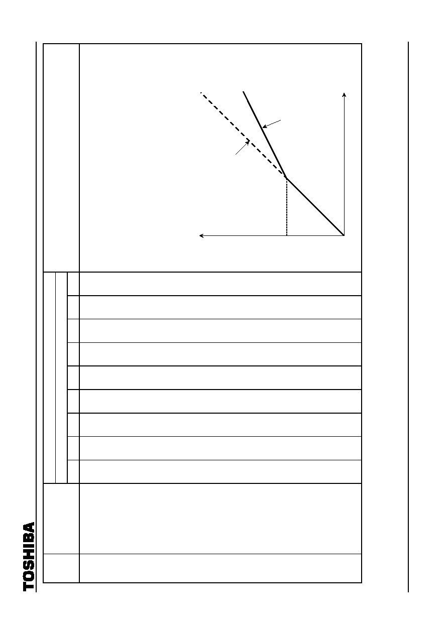
TA1316AN
2002-10-04
83
Test Conditions
SW mode
Note No.
Parameter
SW3
SW4
SW5
SW33 SW34 SW35 SW37 SW38 SW39
Test Method (test conditions: V
CC
= 9 V/2 V, Ta = 25∞ ± 3∞C)
A04
Color
characteristic
C
B
A
A
A
A
A
A
A
(1) Input signal 2 to pin 5.
(2) Increase signal 2 amplitude A. When sub-address (14) data starts with
correction, determine pin 43 output signal amplitudes V
1
, V
2
and V
3
. Graph
the results in the following cases:
(01)
- off
(03)
- 1 on
(05)
- 2 on
(07)
- 3 on
(3) Determine V
where starts applying and gradient ratio at on when
linearity at off is (1).
Pin 43 output amplitude
Pin 5 input
amplitude
V
OFF
ON
TA1316AN
2002-10-04
84
Test Conditions
SW mode
Note No.
Parameter
SW3
SW4
SW5
SW33 SW34 SW35 SW37 SW38 SW39
Test Method (test conditions: V
CC
= 9 V/2 V, Ta = 25∞ ± 3∞C)
A05
Color limiter
characteristic
C
B
A
A
A
A
A
A
A
(1) Input signal 2 (picture period amplitude
= 0.4 V
P-P
) to pin 4.
(2) When sub-address (14) data is 00 and 01, measure pin 43 output signal picture
period amplitudes C
LT0
and C
LT1
.
A06
High bright color gain
C
B
A
A
A
A
A
A
A
(1) Input signal 2 (picture period amplitude
= 0.2 V
P-P
) to pin 4.
(2) Adjust COLOR and set pin 41 output picture period amplitude to 1.2 V
P-P
.
(3) When sub-address (0B) data is 80, measure pin 41 output signal picture period
amplitude V
41
.
(4) Calculate using the following formula. HBC
1
= (1.2 - v
41
)/1.2
TA1316AN
2002-10-04
85
Test Conditions for Text
Common Test Conditions for Text
(1) Unless otherwise specified, measure bus data using preset values.
(2) Set the following data:
Sub-address (00) to data (02)
Sub-address (05) to data (7F)
Sub-address (09) to data (40)
Sub-address (0B) to data (7F)
Sub-address (0C) to data (82)
Sub-address (12) to data (F0)
Sub-address (19) to data (F8)
Sub-address (1A) to data (E0)
Sub-address (1B) to data (E0)
Sub-address (1D) to data (78)
Sub-address (1E) to data (87)
Test Conditions
SW mode
Note
No.
Parameter
SW3
SW4
SW5
SW33 SW34 SW35 SW37 SW38 SW39
Test Method (test conditions: V
CC
= 9 V/2 V, Ta = 25∞ ± 3∞C)
T01 AC gain
A
B
B
A
A
A
A
A
A
(1) Input signal 1 (f
0
= 100 kHz, amplitude of picture period voltage = 0.2 V
P-P
) to pin 3.
(2) Measure pins 41, 42 and 43 picture period amplitudes V
41
, V
42
and V
43
.
(3) Determine AC gain using the following formulae.
G
R
= V
43
/0.2 G
G
= V
42
/0.2 G
B
= V
41
/0.2
T02 Unicolor
adjustment
characteristic
A
B
B
A
A
A
A
A
A
(1) Input signal 1 (f
0
= 100 kHz, amplitude of picture period voltage = 0.2 V
P-P
) to pin 3.
(2) Vary UNI-COLOR data to maximum (7F), center (40) and minimum (00), and measure pin 43
picture period amplitudes V
uMAX
, V
uCNT
and V
uMIN
.
(3) Determine amplitude ratio
V
u
of V
uMAX
to V
uCNT
(in decibels).
T03 Brightness
adjustment
characteristic
A
B
B
A
A
A
A
A
A
(1) Input signal 2 to pin 3 and set pin 43 picture period amplitude to 1 V
P-P
.
(2) Vary BRIGHTNESS to maximum (7F), center (80) and minimum (00), and measure pin 43
voltages V
brMAX
, V
brCNT
and V
brMIN
.
T04 White peak
slice level
C
B
B
A
A
A
A
A
A
(1) Set SUB-CONTRAST to maximum.
(2) Apply external power supply to pin 3 and increase voltage from 5.8 V.
(3) When pin 43 picture period is clipped, measure pin 43 picture period amplitude voltage V
WPS1
.
(4) Repeat steps from (1) to (3) above (for V
WPS2
), changing sub-address (0C) data to 06.
TA1316AN
2002-10-04
86
Test Conditions
SW mode
Note
No.
Parameter
SW3
SW4
SW5
SW33 SW34 SW35 SW37 SW38 SW39
Test Method (test conditions: V
CC
= 9 V/2 V, Ta = 25∞ ± 3∞C)
T05 Black peak
slice level
C
B
B
A
A
A
A
A
A
(1) Apply external power supply to pin 3 and gradually decrease voltage from 5.8 V.
(2) When picture period is clipped, measure V
bps
voltage for pins 41, 42 and 43.
T06 RGB output
S/N
C
B
B
A
A
A
A
A
A
(1) Adjust BRIGHTNESS so that pin 41 picture period voltage is 2.4 V.
(2) Set COLOR to minimum.
(3) Measure pins 41, 42 and 43 picture period noise levels n41, n42 and n43 (V
P-P
) using
oscilloscope.
(4) Calculate S/N.
N
41
= -20 ◊ og [2.3/(0.2 ◊ n41)]
N
42
= -20 ◊ og [2.3/(0.2 ◊ n42)]
N
43
= -20 ◊ og [2.3/(0.2 ◊ n43)]
T07 Half-tone
characteristic
A
B
B
A
A
A
A
A
A
(1) Input signal 1 (f
0
= 100 kHz, amplitude of picture period voltage = 0.2 V
P-P
) to pin 3.
(2) Measure pin 41 picture period amplitude v41A.
(3) Apply 1.5 V to pin 52 from external power supply.
(4) Measure pin 41 picture period amplitude v41B.
(5) Determine G
HT1
= v41B/v41A.
(6) Stop applying voltage to pin 52, set sub-address (1A) data to E2 and measure pin 41 picture
period amplitude v41C.
(7) Determine G
HT2
= v41C/v41A.
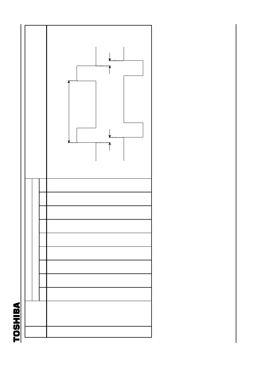
TA1316AN
2002-10-04
87
Test Conditions
SW mode
Note
No.
Parameter
SW3
SW4
SW5
SW33 SW34 SW35 SW37 SW38 SW39
Test Method (test conditions: V
CC
= 9 V/2 V, Ta = 25∞ ± 3∞C)
T08 Blanking pulse
delay time
C
B
B
A
A
A
A
A
A
(1) Apply signal shown in Figure (A) to pin 24 (BLK IN) and determine td
ON
and td
OFF
from
output signal from pins 41, 42 and 43 (Figure (B)).
63.5
µs
td
ON
td
OFF
(A) Signal applied
to pin 24
(B) Output signal
from pins 41,
42 and 43.
TA1316AN
2002-10-04
88
Test Conditions
SW mode
Note
No.
Parameter
SW3
SW4
SW5
SW33 SW34 SW35 SW37 SW38 SW39
Test Method (test conditions: V
CC
= 9 V/2 V, Ta = 25∞ ± 3∞C)
T09 Drive
adjustment
variable range
A
B
B
A
A
A
A
A
A
(1) Input signal 1 (f
0
= 100 kHz, picture period amplitude = 0.2 V
P-P
) to pin 3.
(2) Change sub-address (0D) data to maximum (FE), center (80) and minimum (00), and
measure pin 42 picture period amplitude.
(3) Determine in decibels amplitude ratios of maximum and minimum to drive center (DRG
G1
+
,
DR
G1
-
).
(4) Repeat steps (1) to (3) above, changing sub-address (0E) data to instead, and determine in
decibels pin 41 picture period amplitude ratios (DR
B1
+
, DR
B2
-
).
(5) Repeat steps (1) to (3) above, changing sub-address (0E) data to center (81), and determine
in decibels pin 42 picture period amplitude ratios (DR
G2
+
, DR
G2
-
).
(6) Repeat steps (1) to (3) above, changing sub-address (0E) data to maximum (FF), center (81)
and minimum (01), and determine in decibels pin 41 amplitude ratios (DR
B2
+
, DR
B2
-
).
(7) Repeat steps (1) to (3) above, changing sub-address (0D) data to maximum (FF), center (81)
and minimum (01), and determine in decibels pin 43 amplitude ratios (DR
R1
+
, DR
R1
-
).
(8) Repeat steps (1) to (3) above, setting sub-address (0D) data to 81 and changing sub-address
(0E) data, and determine in decibels pin 41 picture period amplitude ratios (DR
B3
+
, DR
B3
-
).
(9) Repeat steps (1) to (3) above, setting sub-address (0E) data to 81 and changing sub-address
(0D) data to maximum (FF), center (81) and minimum (01), and determine in decibels pin 42
picture period amplitude ratios (DR
G3
+
, DR
G3
-
).
(10) Repeat steps (1) to (3) above, setting sub-address (0D) data to 81 and changing sub-address
(0E) data to maximum (FF), center (81) and minimum (01), and determine in decibels pin 43
picture period amplitude ratios (DR
R2
+
, DR
R2
-
).
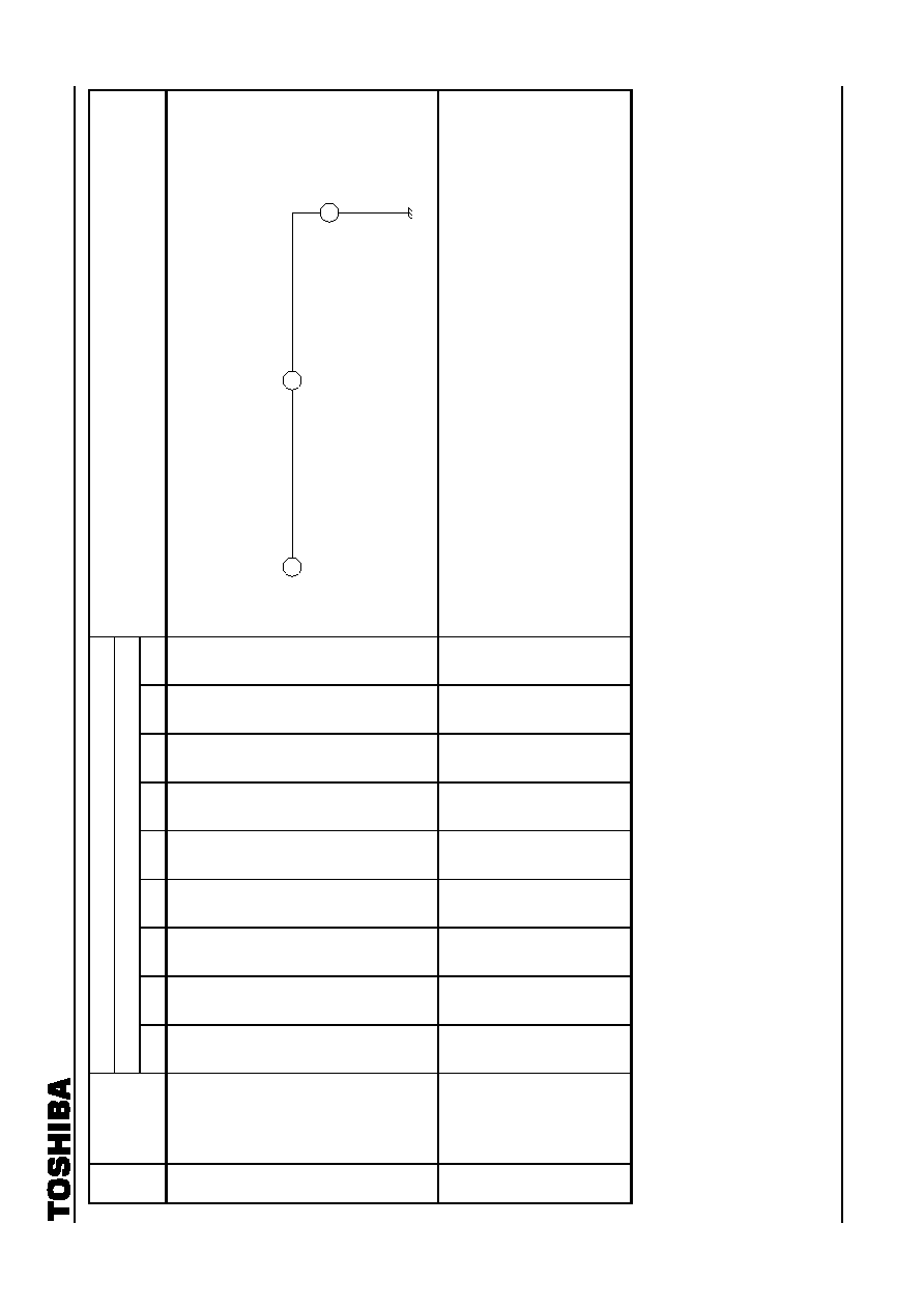
TA1316AN
2002-10-04
89
Test Conditions
SW mode
Note
No.
Parameter
SW3
SW4
SW5
SW33 SW34 SW35 SW37 SW38 SW39
Test Method (test conditions: V
CC
= 9 V/2 V, Ta = 25∞ ± 3∞C)
T10 Pin 53 input
impedance
C
B
B
A
A
A
A
A
A
(1) Connect external power supply, voltmeter and ammeter as shown below. Adjust voltage so
that current value is 0.
(2) Increase pin 53 voltage by 0.2 V and measure current value of ammeter I
in
.
(3) Determine Z
in53
= 0.2 V/I
in
(
).
T11 ACL
characteristic
C
B
B
A
A
A
A
A
A
(1) Input signal 1 (f
0
= 100 kHz, picture period amplitude = 0.2 V
P-P
) to pin 3.
(2) Measure pin 43 picture period amplitude vACL1.
(3) Apply external power supply (pin 53 DC voltage
- 0.5 V) to pin 53 and measure pin 43
picture period amplitude vACL2.
(4) Apply external power supply (pin 53 DC voltage
- 1 V) to pin 53 and measure pin 43 picture
period amplitude vACL3.
(5) Calculate using the following formulae.
ACL
1
= -20 ◊ og (vACL2/vACL1)
ACL
2
= -20 ◊ og (vACL3/vACL1)
-
+
Ammeter (
µA)
Voltmeter
53
A
V
TA1316AN
2002-10-04
90
Test Conditions
SW mode
Note
No.
Parameter
SW3
SW4
SW5
SW33 SW34 SW35 SW37 SW38 SW39
Test Method (test conditions: V
CC
= 9 V/2 V, Ta = 25∞ ± 3∞C)
T12 ABL point
C
B
B
A
A
A
A
A
A
(1) Measure pin 53 DC voltage VABL1.
(2) Set sub-address (1B) data to 1C.
(3) Apply external power supply to pin 53 and decrease voltage from 6.5 V. When pin 43 voltage
starts changing, measure pin 53 voltage VABL2.
(4) Repeat step (3) above, making the following changes:
Set sub-address (1B) data to 3C, 5C, 7C, 9C, BC, DC and FC and measure the following
voltages on pin 53: VABL3, VABL4, VABL5, VABL6, VABL7, VABL8 and VABL9.
(5) ABL
P1
= VABL2 - VABL1
ABL
P5
= VABL6 - VABL1
ABL
P2
= VABL3 - VABL1
ABL
P6
= VABL7 - VABL1
ABL
P3
= VABL4 - VABL1
ABL
P7
= VABL8 - VABL1
ABL
P4
= VABL5 - VABL1
ABL
P8
= VABL9 - VABL1
T13 ABL gain
C
B
B
A
A
A
A
A
A
(1) Apply external power supply of 6.5 V to pin 53.
(2) Set sub-address (1B) data to 00.
(3) Set BRIGHTNESS to maximum.
(4) Apply external power supply of 4.5 V to pin 53.
(5) Repeat step (3) above, making the following changes:
Set sub-address (1B) data to 00, 04, 08, 0C, 10, 14, 18 and 1C and measure the following
voltages on pin 53: VABL11, VABL12, VABL13, VABL14, VABL15, VABL16, VABL17 and
VABL18.
(6) ABL
G1
= VABL11 - VABL10
ABL
G2
= VABL12 - VABL10
ABL
G3
= VABL13 - VABL10
ABL
G4
= VABL14 - VABL10
ABL
G5
= VABL15 - VABL10
ABL
G6
= VABL16 - VABL10
ABL
G7
= VABL17 - VABL10
ABL
G8
= VABL18 - VABL10
TA1316AN
2002-10-04
91
Test Conditions
SW mode
Note
No.
Parameter
SW3
SW4
SW5
SW33 SW34 SW35 SW37 SW38 SW39
Test Method (test conditions: V
CC
= 9 V/2 V, Ta = 25∞ ± 3∞C)
T14 RGB output
mode
C
B
B
A
A
A
A
A
A
(1) Adjust BRIGHTNESS so that pin 43 picture period voltage becomes 2.4 V.
(2) Set sub-address (1B) data to 01.
(3) Measure picture period voltages V
43R
, V
42R
and V
41R
on pins 43, 42 and 41 respectively.
(4) Repeat step (3) above, changing sub-address (1B) data to 02, and measure picture period
voltages V
43G
, V
42G
and V
41G
on pins 43, 42 and 41 respectively.
(5) Repeat step (3), changing sub-address (1B) data to 03, and measure picture period voltages
V
43B
, V
42B
and V
41B
on pins 43, 42 and 41 respectively.
TA1316AN
2002-10-04
92
Test Conditions
SW mode
Note
No.
Parameter
SW3
SW4
SW5
SW33 SW34 SW35 SW37 SW38 SW39
Test Method (test conditions: V
CC
= 9 V/2 V, Ta = 25∞ ± 3∞C)
T15 Y-OUT
characteristic
A
B
B
A
A
A
A
A
A
(1) Input ramp waveform to pin 3 and adjust input amplitude so that pin 43 picture period
amplitude becomes 2.3 V
P-P
.
(2) Set sub-address (1C) data to 01.
(3) Adjust input amplitude so that pin 43 picture period amplitude becomes 2.3 V
P-P
.
(4) According to the figure below, determine in decibels Y-OUT
correction start points 1 and 2
and gradient ratios
1, 2 and 3, which are ratios of gradient at -on to gradient at -off.
100 IRE
2
1
Output amplitude (Y-OUT)
Input amplitude
2.3 V
p-p
1
2
3
Note: Solid line:
-off
Dotted line:
-on
TA1316AN
2002-10-04
93
Test Conditions
SW mode
Note
No.
Parameter
SW3
SW4
SW5
SW33 SW34 SW35 SW37 SW38 SW39
Test Method (test conditions: V
CC
= 9 V/2 V, Ta = 25∞ ± 3∞C)
T16 Blue stretch
circuit
characteristic
A
B
B
A
A
A
A
A
A
(1) Input ramp signal of 0.7 V
P-P
to pin 3.
(2) Set SUB-CONTRAST to maximum.
(3) Set sub-address (1F) data to 04.
(4) Set sub-address (1E) data to 00 and determine blue stretch start point BS
P
min
using pin 41
in the figure below.
(5) Repeat step (4) above, changing sub-address (1E) data to 04 and 07. Determine blue stretch
start points BS
P
CNT and BS
P
max.
(6) Set sub-address (1E) data to 04.
(7) Determine in decibels ratio of gradient at blue stretch on to gradient at blue stretch off, using
pin 41 as shown in the figure below.
(8) Repeat step (7) above, changing sub-address (1F) data to 00 and 07, and determine in
decibels gradient ratios BS
G
min and BS
G
max.
Note: The blue stretch start point is determined as an IRE value by setting the amplitude from the
output signal pedestal level to the positive side to be 2.3 V
P-P
= 100 IRE.
Blue stretch on
Blue stretch off
Blue stretch start point
Output amplitude
Input amplitude
(Pin 41 output)
TA1316AN
2002-10-04
94
Test Conditions
SW mode
Note
No.
Parameter
SW3
SW4
SW5
SW33 SW34 SW35 SW37 SW38 SW39
Test Method (test conditions: V
CC
= 9 V/2 V, Ta = 25∞ ± 3∞C)
T17 ACB pulse
phase and
amplitude
A
or
C
B
B
A
A
A
A
A
A
(1) Input signal 1 (f
0
= 100 kHz, picture period amplitude = 0.2 V
P-P
) to pin 3. Adjust DRIVE
GAIN 1/2 so that pin 41/42 picture period amplitude is equal to that of pin 43.
(2) Measure voltage of pins 46, 47 and 48 and apply measured voltages from external power
supply to pins.
(3) Set sub-address (02) data to 40.
(4) Determine ACB pulse phase by referencing signal waveform output from pins 43, 42 and 41
as shown in Figure 1 below.
Note: The first picture period after V-BLK ends and FBP input falls is 1H. After each H-BLK, the
phase is 2H, 3H and so on.
(5) Determine ACB pulse amplitudes VACB1R, VACB1G and VACB1B by referencing signal
waveform output from pins 43, 42 and 41. (Amplitude is based on picture period level at no
input.)
(6) Repeat step (5) above, setting sub-address (02) data to 80, and measure VACB2R, VACB2G
and VACB2B.
(7) Repeat step (5) above, setting sub-address (02) data to C0, and measure VACB3R,
VACB3G and VACB3B.
Figure 1 RGB output
ACB pulse amplitude
1H
2H
3H
4H
V-BLK period
Figure 2 FBP input (pin 24)
TA1316AN
2002-10-04
95
Test Conditions
SW mode
Note
No.
Parameter
SW3
SW4
SW5
SW33 SW34 SW35 SW37 SW38 SW39
Test Method (test conditions: V
CC
= 9 V/2 V, Ta = 25∞ ± 3∞C)
T18 IK input
amplitude
A
or
C
B
B
A
A
A
A
A
A
(1) Input signal 1 (f
0
= 100 kHz, picture period amplitude = 0.2 V
P-P
) to pin 3. Adjust DRIVE
GAIN 1/2 so that pin 41/42 picture period amplitude is equal to that of pin 43.
(2) Set sub-address (02) data to 40.
(3) Determine voltage amplitudes while ACB pulse is being applied to pin 45 input signal as
shown in Figure 1 of T19 above.
At 1H
= IK
R
, at 2H
= IK
G
and at 3H
= IK
B
T19 IK input cover
range
C
B
B
A
A
A
A
A
A
(1) Input signal 1 (f
0
= 100 kHz, picture period amplitude = 0.2 V
P-P
) to pin 3 and adjust DRIVE
GAIN 1/2 so that pin 41/42 picture period amplitude is equal to that of pin 43.
(2) Set sub-address (02) data to 40.
(3) Determine DC voltage of pin 45 during V-BLK (#45VBLK).
(4) Apply external voltage via 10 k
and gradually increase the voltage from 0 V.
(5) Determine DC voltage of pin 45 during V-BLK when picture period amplitude of pin 43 has
just started decreasing (#45VBLK
+).
(6) Reset the external voltage to 0 V and gradually decrease from 0 V.
(7) Determine DC voltage of pin 45 during V-BLK when picture period amplitude of pin 43 has
just started increasing (#45VBLK
-).
(8) DIK
in
+
= (#45VBLK+) - (#45VBLK)
DIK
in
-
= (#45VBLK-) + (#45VBLK)
T20 Analog RGB
gain
A
B
B
A
or
B
A
or
B
A
or
B
A
A
A
(1) Input signal 1 (f
0
= 100 kHz, picture period amplitude = 0.2 V
P-P
) to pin 3 and adjust DRIVE
GAIN 1/2 so that pin 41/42 picture period amplitude is equal to that of pin 43.
(2) Apply 5 V from external power supply to pin 49.
(3) Input signal 1 (f
0
= 100 kHz, picture period amplitude = 0.2 V
P-P
) to pin 35.
(4) Measure picture period amplitude v43R on pin 43.
(5) Repeat steps (3) and (4), making the following changes.
Input signal 1 to pin 34 and measure pin 42 output (v42G).
Input signal 1 to pin 33 and measure pin 41 output (v41B).
(6) Calculate using the following formulae.
GTXR
= v43R/0.2 GTXG = v42G/0.2 GTXB = v41B/0.2

TA1316AN
2002-10-04
96
Test Conditions
SW mode
Note
No.
Parameter
SW3
SW4
SW5
SW33 SW34 SW35 SW37 SW38 SW39
Test Method (test conditions: V
CC
= 9 V/2 V, Ta = 25∞ ± 3∞C)
T21 Analog RGB
white peak
slice level
A
B
B
A
A
A
A
A
A
(1) Apply 5 V from external power supply to pin 49.
(2) Set RGB CONTRAST to maximum (7F).
(3) Apply external power supply to pin 35. Gradually increase voltage from 3.0 V DC. When pin
43 output is clipped, measure picture period amplitude.
(4) Repeat step (3), making the following changes:
Input to pin 34 and measure pin 42 output; input to pin 33 and measure pin 41 output.
T22 Analog RGB
black peak
limit level
A
B
B
A
A
A
A
A
A
(1) Apply 5 V from external power supply to pin 49.
(2) Set RGB CONTRAST to maximum (7F).
(3) Apply external power supply to pin 35. Gradually increase voltage from 4.5 V DC. When pin
43 output is clipped, measure picture period amplitude.
(4) Repeat step (3), making the following changes:
Input to pin 34 and measure pin 42 output; input to pin 33 and measure pin 41 output.
T23 RGB contrast
adjustment
characteristic
A
B
B
A
or
B
A
or
B
A
or
B
A
A
A
(1) Apply 5 V from external power supply to pin 49.
(2) Input signal 1 (f
0
= 100 kHz, picture period amplitude = 0.2 V
P-P
) to pin 35.
(3) Change RGB CONTRAST to maximum (7F), center (40) and minimum (00), and measure
picture period amplitude output V
uTXR
(max, CNT and min) on pin 43.
(4) Determine in decibels amplitude ratios of maximum and minimum to center.
(5) Repeat steps (3) and (4), making the following changes:
Input to pin 34 and measure picture period amplitude output on pin 42.
Input to pin 33 and measure picture period amplitude output on pin 41.
T24 Analog RGB
brightness
adjustment
characteristic
A
B
B
A
or
B
A
or
B
A
or
B
A
A
A
(1) Input signal 2 to pins 33, 34 and 35.
(2) Apply 5 V from external power supply to pin 49.
(3) Adjust signal 2 amplitude (A) so that pin 43 picture period amplitude becomes 0.5 V
P-P
.
(4) Change RGB BRIGHTNESS to maximum (FE), center (80) and minimum (00), and measure
picture period voltage output V
brTX
(max, CNT and min) on pins 43, 42 and 41 respectively.
T25 Analog RGB
mode
switching
transfer
characteristic
C
B
B
A
A
A
A
A
A
(1) Set RGB BRIGHTNESS to maximum (FE).
(2) Input signal 4 (signal amplitude
= 1.5 V
P-P
) to pin 49.
(3) Measure input/output transfer characteristic using pin 43 in Figure T-2.
(4) Repeat steps (2) and (3) above, making the following changes:
Input to pin 34 and measure pin 42; input to pin 33 and measure pin 41.
(5) Determine maximum inter-axial rise/fall transfer delay time, using the data measured above.
TA1316AN
2002-10-04
97
Test Conditions
SW mode
Note
No.
Parameter
SW3
SW4
SW5
SW33 SW34 SW35 SW37 SW38 SW39
Test Method (test conditions: V
CC
= 9 V/2 V, Ta = 25∞ ± 3∞C)
T26 Text ACL
characteristic
A
B
B
A
A
B
A
A
A
(1) Apply 5 V from external power supply to pin 49.
(2) Input signal 1 (f
0
= 100 kHz, picture period amplitude = 0.2 V
P-P
) to pin 35.
(3) Measure pin 43 picture period amplitude vTXACL1.
(4) Apply external power supply (pin 53 DC voltage
- 0.5 V) to pin 53 and measure picture
period amplitude output vTXACL2 on pin 43.
(5) Apply external power supply (pin 53 DC voltage
- 1.0 V) to pin 53 and measure picture
period amplitude output vTXACL3 on pin 43.
(6) TXACL
1
= -20 ◊ og (vTXACL2/vTXACL1)
TXACL
2
= -20 ◊ og (vTXACL3/vTXACL1)
(7) Repeat steps (5) and (6), setting sub-address (10) data to 01 to ascertain TXACL
3
and
TXACL
4.
T27 Analog OSD
gain
A
B
B
A
A
A
A
or
B
A
or
B
A
or
B
(1) Input signal 1 (f
0
= 100 kHz, picture period amplitude = 0.2 V
P-P
) to pin 3 and adjust DRIVE
GAIN 1/2 so that pin 41/42 picture period amplitude is equal to that of pin 43.
(2) Apply 5 V from external power supply to pins 50 and 51.
(3) Input signal 1 (f
0
= 100 kHz, picture period amplitude = 0.2 V
P-P
) to pin 39.
(4) Adjust output picture period amplitude v43R on pin 43.
(5) Repeat steps (3) and (4), making the following changes:
Input to pin 38 and measure picture period amplitude output on pin 42 (v42G).
Input to pin 37 and measure picture period amplitude output on pin 41 (v41B).
(6) Calculate using the following formulae.
G
OSDR
= v43R/0.2
G
OSDG
= v42G/0.2
G
OSDB
= v41B/0.2
T28 Analog OSD
white peak
slice level
A
B
B
A
A
A
A
A
A
(1) Apply 5 V from external power supply to pins 50 and 51.
(2) Apply external power supply to pin 39 and gradually increase voltage from 4.5 V DC. When
pin 43 output is clipped, measure picture period amplitude.
(3) Repeat step (2), making the following changes:
Input to pin 38 and measure picture period amplitude output on pin 42.
Input to pin 37 and measure picture period amplitude output on pin 41.
T29 Analog OSD
black peak
limit level
A
B
B
A
A
A
A
A
A
(1) Apply 5 V from external power supply to pins 50 and 51.
(2) Apply external power supply to pin 39 and gradually decrease voltage from 4.5 V DC. When
pin 43 output is clipped, measure picture period amplitude.
(3) Repeat step (2), making the following changes.
Input to pin 38 and measure picture period amplitude output on pin 42.
Input to pin 37 and measure picture period amplitude output on pin 41.

TA1316AN
2002-10-04
98
Test Conditions
SW mode
Note
No.
Parameter
SW3
SW4
SW5
SW33 SW34 SW35 SW37 SW38 SW39
Test Method (test conditions: V
CC
= 9 V/2 V, Ta = 25∞ ± 3∞C)
T30 Analog OSD
contrast
adjustment
characteristic
A
B
B
A
A
A
A
or
B
A
or
B
A
or
B
(1) Apply 5 V from external power supply to pins 50 and 51.
(2) Input signal 1 (f
0
= 100 kHz, picture period amplitude = 0.2 V
P-P
) to pin 39.
(3) Change OSD-CONTRAST to (11), (10), (01) and (00) and measure picture period amplitude
outputs V
uOSDR
(11), (10), (01) and (00) on pin 43.
(4) Repeat steps (2) and (3), making the following changes:
Input to pin 38 and measure picture period amplitude outputs V
uOSDG
(11), (10), (01) and
(00) on pin 42.
Input to pin 37 and measure picture period amplitude outputs V
uOSDB
(11), (10), (01) and
(00) on pin 41.
T31 Analog OSD
brightness
adjustment
characteristic
C
B
B
A
A
A
A
A
A
(1) Apply 5 V from external power supply to pins 50 and 51.
(2) Change OSD BRIGHT (sub-address 1D) to (38), (78), (B8) and (F8) and measure picture
period voltage outputs on pins 43, 42 and 41.
Data (38)
- V
brOSD0
Data (78)
- V
brOSD1
Data (B8)
- V
brOSD2
Data (F8)
- V
brOSD3
T32 Analog OSD
mode
switching
transfer
characteristic
C
B
B
A
A
A
A
A
A
(1) Set OSD BRIGHT to maximum (11).
(2) Input signal 4 (signal amplitude
= 4.5 V
P-P
) to pin 50.
(3) Measure input/output transfer characteristic, using pin 43 as shown in Figure T-2.
(4) Repeat steps (2) and (3) above, and measure pins 42 and 41.
(5) Determine maximum inter-axial rise/fall transfer delay time, using the data measured above.
(6) Repeat steps (1) to (5), inputting signal 4 (signal amplitude
= 4.5 V
P-P
) to pin 51, and
measure.

TA1316AN
2002-10-04
99
Test Conditions
SW mode
Note
No.
Parameter
SW3
SW4
SW5
SW33 SW34 SW35 SW37 SW38 SW39
Test Method (test conditions: V
CC
= 9 V/2 V, Ta = 25∞ ± 3∞C)
T33 OSD ACL
characteristic
A
B
B
A
A
A
A
A
B
(1) Set sub-address (07) data to 01.
(2) Apply 5 V from external power supply to pins 50 and 51.
(3) Input signal 1 (f
0
= 100 kHz, picture period amplitude = 0.2 V
P-P
) to pin 39.
(4) Measure picture period amplitude vOSDACL1 on pin 43.
(5) Apply external power supply (pin 53 DC voltage
- 0.5 V) to pin 53 and measure picture
period amplitude vOSDACL2 on pin 43.
(6) Apply external power supply (pin 53 DC voltage
- 1 V) to pin 53 and measure picture period
amplitude vOSDACL3 on pin 43.
(7) OSDACL
1
= -20 ◊ og (vOSDACL2/vOSDACL1)
OSDACL
2
= -20 ◊ og (vOSDACL3/vOSDACL1)
(8) Repeat steps (5) and (6) above, changing sub-address (07) data to 00, and measure
OSDACL3 and OSDACL4.
TA1316AN
2002-10-04
100
Test Conditions
SW mode
Note
No.
Parameter
SW3
SW4
SW5
SW33 SW34 SW35 SW37 SW38 SW39
Test Method (test conditions: V
CC
= 9 V/2 V, Ta = 25∞ ± 3∞C)
T34 OSD blending
characteristic
A
C
B
B
A
A
A
A
B
A
B
B
B
(1) Input signal 1 (f
0
= 100 kHz, picture period amplitude = 0.2 V
P-P
) to pin 3.
(2) Measure picture period amplitudes v41a, v42a and v43a on pins 41, 42 and 43 respectively.
(3) Apply 5 V from external power supply to pin 51.
(4) Measure picture period amplitudes v41b, v42b and v43b on pins 41, 42 and 43 respectively.
(5) Determine in decibels v41b amplitude in relation to v41a; v42b amplitude in relation to v42a;
v43b amplitude in relation to v43a:
41TV1, 42TV1 and 43TV1.
(6) Repeat steps (3) to (5), applying 5 V from external power supply to pin 50, and measure
41TV2, 42TV2 and 43TV2.
(7) Repeat steps (3) to (5), applying 5 V from external power supply to pins 50 and 51, and
measure
41TV3, 42TV3 and 43TV3.
(8) Set to SW3 to C; SW37, SW38, Sw39 to B.
(9) Input signal 1 (f
0
= 100 kHz, picture period amplitude = 0.2 V
P-P
) to pins 37, 38 and 39.
(10) Apply 5 V from external power supply to pins 50 and 51.
(11) Measure picture period amplitudes v41c, v42c and v43c on pins 41, 42 and 43 respectively.
(12) Apply 5 V from external power supply to pin 50.
(13) Measure picture period amplitudes v41d, v42d and v43d on pins 41, 42 and 43 respectively.
(14) Determine in decibels v41d amplitude in relation to v41c; v42d amplitude in relation to v42c;
v43d amplitude in relation to v43c:
41OSD1, 42OSD1 and 43OSD1.
(15) Repeat steps (12) to (14), applying 5 V from external power supply to pin 51, and measure
41OSD2, 42OSD2 and 43OSD2.
(16) Repeat steps (12) to (14), applying 5 V from external power supply to pins 50 and 51, and
measure
41OSD3, 42OSD3 and 43OSD3.
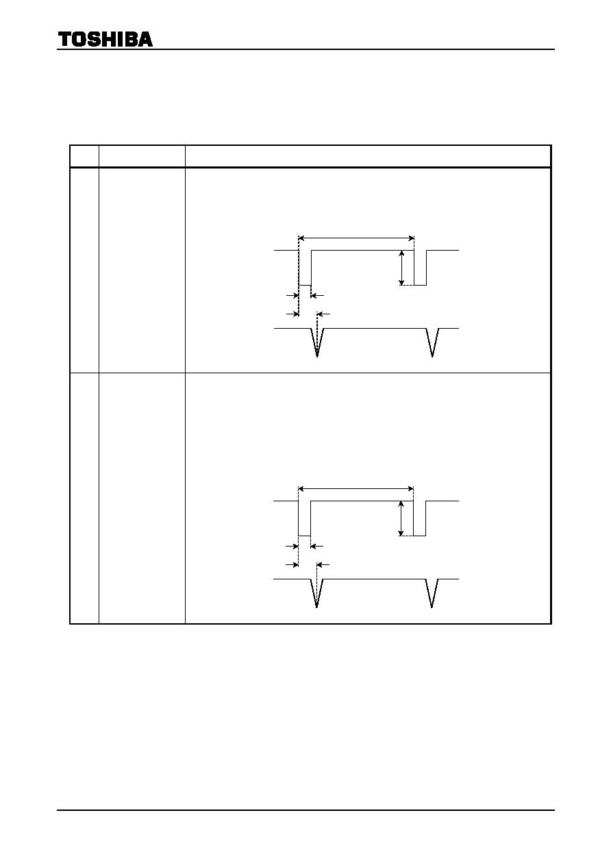
TA1316AN
2002-10-04
101
Test Conditions for Deflection
Common Test Conditions for Sync Signal
(Unless otherwise specified, V
CC
=
=
=
= 9 V/2 V, Ta ==== 25∞C, BUS data ==== preset values.)
(Unless otherwise specified, SW3
=
=
=
= A, SW14 ==== A, SW20 ==== on, SW22 ==== open, SW23 ==== B, SW24a ==== B,
SW24b
=
=
=
= open and SW26 ==== B.)
Note
No.
Parameter
Test Method
HA01 Sync input horizontal
sync phase
(1) Input signal a (as shown in figure below) to TPA. Set sub-address (00) data to 82H.
(2) Determine phase difference S
1PH
from pin 14 (SYNC IN) input waveform and pin 20 (AFC
filter) waveform.
HA02 HD 1/2 input
horizontal sync phase
(1) Set sub-address (00) data to 40H.
(2) Input signal b (as shown in figure below) to TP16.
(3) Determine phase difference HD
1PH
from pin 16 (HD1 IN) input waveform and pin 20 (AFC
filter) waveform.
(4) Input signal b to TP13 and set sub-address (00) data to 41H.
(5) Determine phase difference HD
2PH
as in step (3) above.
29.36
µs
0.285 V
0.593
µs
Signal a
Pin 20 waveform
S
PH
31.75
µs
1.5 V
2.35
µs
Signal b
Pin 20 waveform
HD
1PH
, HD
2PH

TA1316AN
2002-10-04
102
Note
No.
Parameter
Test Method
HA03 Polarity detection
range
(1) Set sub-address (00) data to 40H.
(2) Input signal b (as shown in figure below) to TP16.
(3) Decrease signal b duty from 10% (to shorter negative polarity period) and determine signal b
duty (HD
DUTY1
) when pin 16 input signal phase no longer locks with that of pin 26 (H-OUT).
(4) Increase signal b duty from 10% (to longer negative polarity period) and determine signal b
duty (HD
DUTY2
) when pin 24 (FBP IN) phase changes in relation to signal b.
(5) Further increase signal b duty (to longer negative polarity period) and determine signal b duty
(HD
DUTY3
) when pin 16 input signal phase no longer locks with that of pin 26 (H-OUT).
(6) Decrease signal b duty from 90% (to shorter negative polarity period) and determine signal b
duty (HD
DUTY4
) when pin 24 (FBP IN) phase changes in relation to signal b.
Duty
= A/B ◊ 100% (0%~100%)
HA04 Sync input threshold
amplitude
(1)
Set sub-address (00) to 82H and TEST mode to 01.
(2) Apply external voltage via 20 k
to pin 14.
(3) Set external voltage to 0 V and monitor pin 14 pin voltage SYNC_TIP_00.
Also check that pin 28 pin voltage is L.
(4) By increasing external voltage SYNC_OFF_00, monitor pin 14 SYNC IN pin voltage when pin
28 DAC1 pin voltage becomes H.
(5) Determine SYNC input level at SYNC separation level 00 as follows:
V
ths00
= (SYNC_OFF_00 - SYNC_TIP_00) /0.286 ◊ 100
(6) Set SYNC separation level from 01 to 10 to 11, and determine V
ths01
, V
ths10
and V
ths11
.
V
ths01
= (SYNC_OFF_01 - SYNC_TIP_01) /0.286 ◊ 100
V
ths10
= (SYNC_OFF_10 - SYNC_TIP_10) /0.286 ◊ 100
V
ths11
= (SYNC_OFF_11 - SYNC_TIP_11) /0.286 ◊ 100
31.75
µs
1.5 V
Signal b
A
B
1H
Pin 14
0.08H
40 IRE
(
= 286
mV
p-p
)
Pin 28
(SYNC output Mode)
Sync Tip level
Sync Sepa level
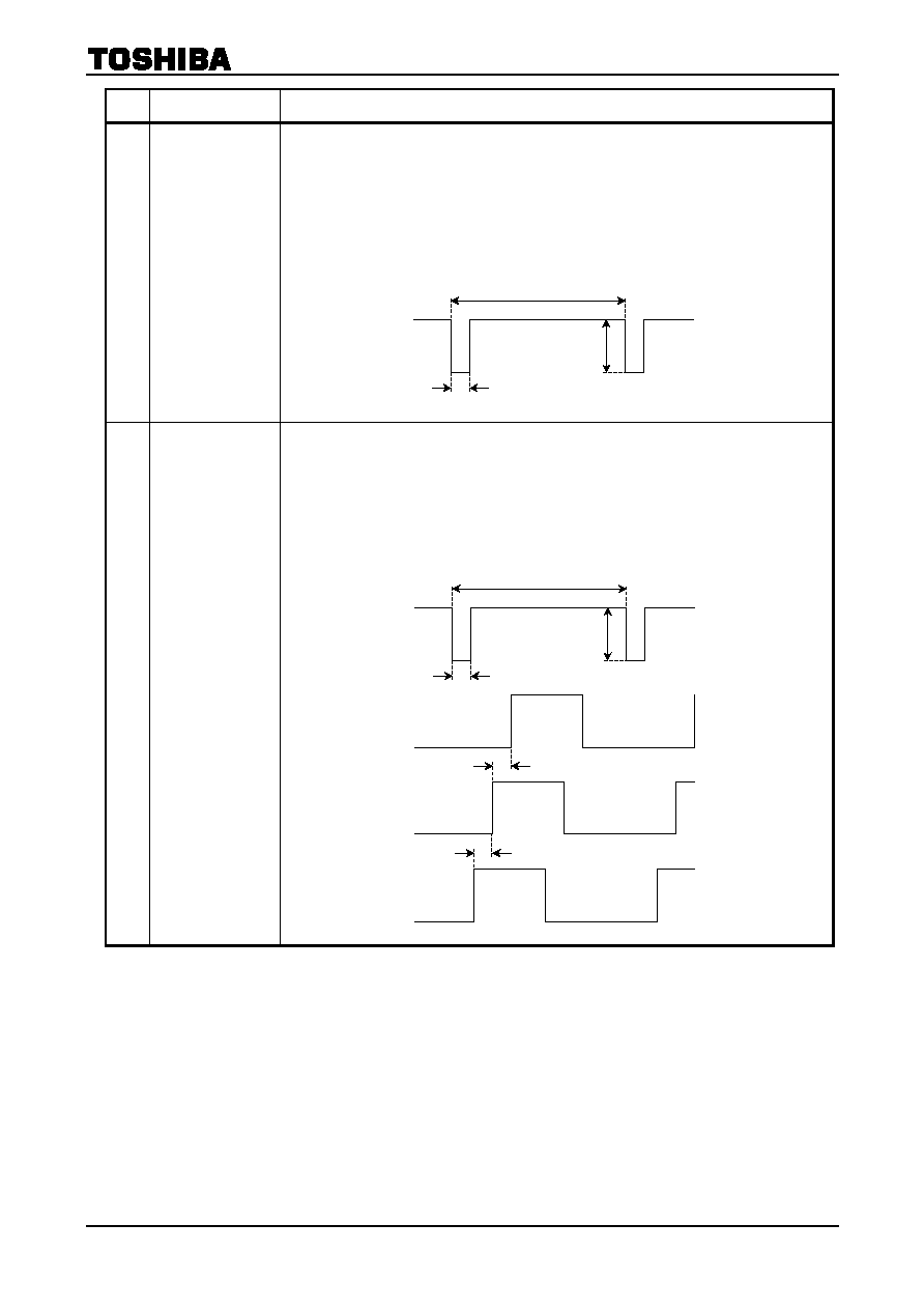
TA1316AN
2002-10-04
103
Note
No.
Parameter
Test Method
HA05 HD 1/2 input
threshold voltage
(1) Set sub-address (00) data to 40H.
(2) Input signal b (as shown in figure below) to TP16.
(3) Increase signal b amplitude from 0 V
P-P
. When pin 26 (H-OUT) phase locks with that of signal
b, determine signal b amplitude V
thHD1
.
(4) Input signal b (as shown in figure below) to TP13 and set sub-address (00) data to 41H.
(5) Measure as in step (3) above, and determine signal amplitude V
thHD2
.
HA06 Horizontal picture
phase adjustment
variable range
(1) Set sub-address (00) data to 40H.
(2) Input signal b (as shown in figure below) to TP16.
(3) Change sub-address (01) data from 80H to 00H and measure pin 26 (H-OUT) waveform
phase change
H
SFT
-
.
(4) Change sub-address (01) data from 80H to FEH and measure pin 26 (H-OUT) waveform
phase change
H
SFT
+
.
31.75
µs
V
thDH
2.35
µs
Signal b
31.75
µs
1.5 V
2.35
µs
Signal b
Pin 26 waveform
Data: 00H
H
SFT
-
H
SFT
+
Pin 26 waveform
Data: FEH
Pin 26 waveform
Data: 80H
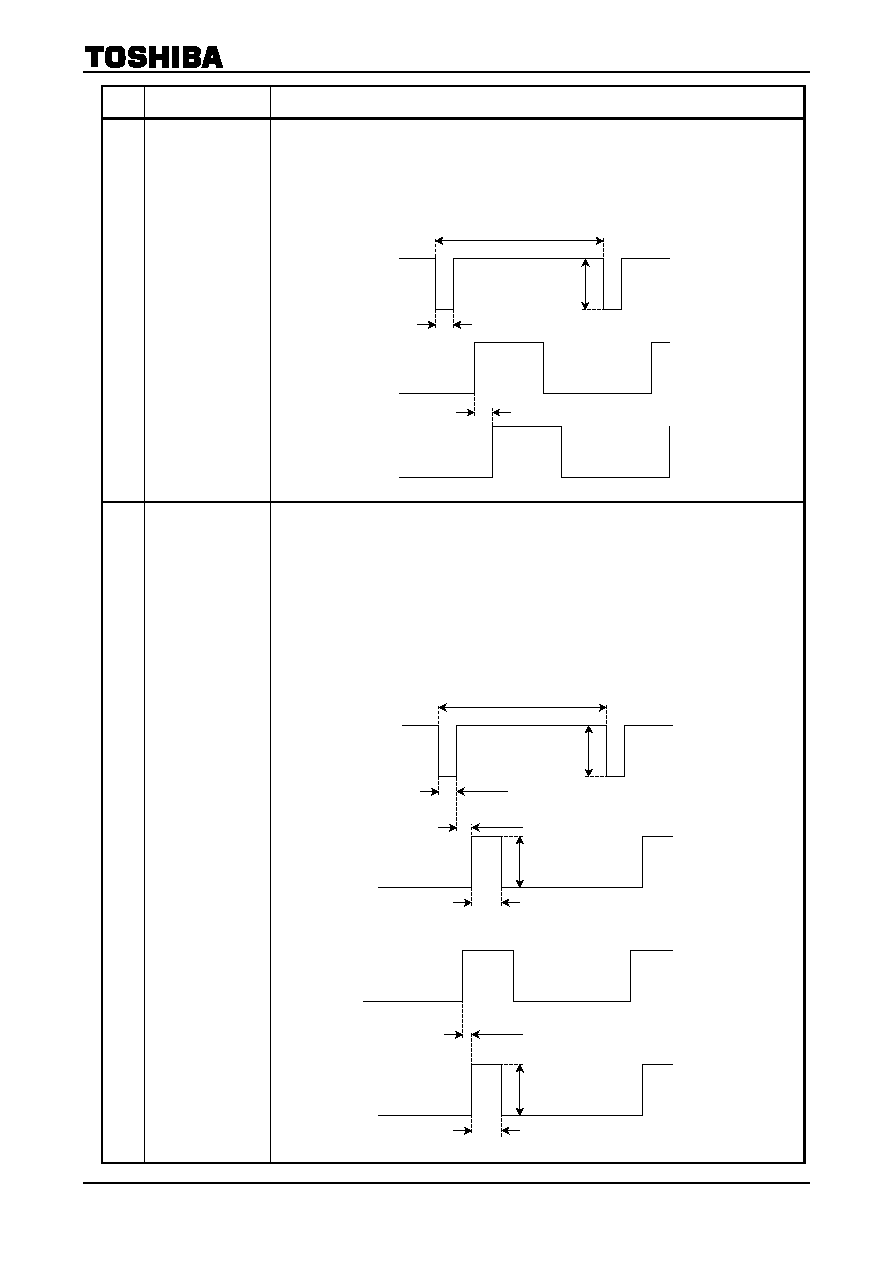
TA1316AN
2002-10-04
104
Note
No.
Parameter
Test Method
HA07 Curve correction
(1) Set sub-address (00) data to 40H.
(2) Input signal b (as shown in figure below) to TP16.
(3) Connect external power supply to pin 23 (H CURVE CORRECTION). Apply 1.5 V and 3.5 V to
pin 23 and measure the output waveform phase change
H
#23
on pin 26 (H-OUT).
HA08 Clamp pulse phase,
width and level
(1) Set sub-address (00) data to 40H.
(2) Input signal b (as shown in figure below) to TP16.
(3) Determine clamp pulse phase CP
S0
, width CP
PW0
and output level CP
V0
on pin 18 (SCP
OUT) in relation to signal b.
(4) Set sub-address (01) data to 81H. Determine CP
S1
, CP
PW1
and CP
V1
as in step (3) above.
(5) Apply no signal input to TP16.
(6) Determine pin 18 clamp pulse phase CP
S2
, width CP
PW2
and output level CP
V2
in relation to
pin 24.
31.75
µs
1.5 V
2.35
µs
Signal b
Pin 26 waveform
(pin 23 voltage: 1.5 V)
H
#23
Pin 26 waveform
(pin 23 voltage: 3.5 V)
31.75
µs
1.5 V
2.35
µs
Signal b
Pin 18 waveform
Pin 24 waveform
CP
V0/1
CP
W0/1
CP
S0/1
Pin 18 waveform
CP
V2
CP
W2
CP
S2
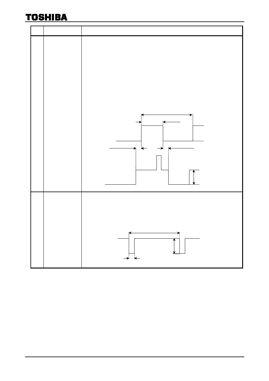
TA1316AN
2002-10-04
105
Note
No.
Parameter
Test Method
HA09 Black peak detection
pulse phase and level
(1) Set sub-address (00) data to 40H.
(2) Set SW24A to open.
(3) Input signal c (as shown in figure below) to pin 24 (FBP IN).
(4) Determine pin 18 (SCP OUT) black peak detection pulse phase HBP
S0a
and HBP
S0b
in
relation to signal c.
(5) Determine output level HBP
SV0
from pin 18 (SCP OUT) output waveform.
(6) Set sub-address (02) data to 90H.
(7) Measure as in steps (4) and (5), and determine phases HBP
S1a
and HBP
S1b
, and output level
HBP
SV1
.
(8) Change sub-address (00) data to C0H and sub-address (02) data to 80H, and determine
phases HBP
S45a
and HBP
S45b
, and output level HBP
SV45
.
HA10 FBP threshold
(1) Set sub-address (00) data to 40H.
(2) Input signal b (as shown in figure below) to TP16.
(3) Increase amplitude of FBP signal input to pin 24 (FBP IN) from 0 V
P-P
. When signal b and pin
26 (H-OUT) phases are locked, measure pin 24 input amplitude (V
thFBP
).
31.75
µs
1.5 V
2.35
µs
31.5
µs
2 V
0 V
HBP
SV0/SV1/SV45
Signal c
Pin 18 waveform
4.13
µs
HBP
S0b/S1b/S45b
HBP
S0a/S1a/S45a

TA1316AN
2002-10-04
106
Note
No.
Parameter
Test Method
HB01 H-OUT pulse duty
(1) No signal input.
(2) Measure T1 and T2 (as shown in figure below) from pin 26 (H-OUT) output waveform when
sub-address (00) data is 80H and A0H. Determine duties TH
00A
and TH
00B
using the
following formula:
TH
= T1/(T1 + T2) ◊ 100 %
(3) Set sub-address (00) data to 81H, A1H, 82H and A2H, measure as in step (2) above, and
determine duties TH
01A
, TH
01B
, TH
10A
and TH
10B
.
HB02 Horizontal
free-running
frequency
(1) Set SW20 to open.
(2) Set sub-address (00) data to 00H and measure horizontal free-running frequency F00 from pin
26 (H-OUT) output waveform.
(3) Set sub-address (00) data to 40H, 80H and C0H, measure as in step (2) above, horizontal
free-running frequencies F01, F10 and F11.
HB03 Horizontal oscillation
frequency variable
range
(1) Set sub-address (00) data to 00H.
(2) Connect 10-k
resistor between pin 20 and V
CC
. Measure horizontal frequency F00
MIN
from
pin 26 (H-OUT) output waveform.
(3) Connect 68-k
resistor between pin 20 and GND. Measure horizontal frequency F00
MAX
from
pin 26 (H-OUT) output waveform.
(4) Set sub-address (00) data to 40H, 80H and C0H, and measure as in steps (2) and (3) above,
horizontal frequencies F01
MIN
, F01
MAX
, F10
MIN
, F10
MAX
, F11
MIN
and F11
MAX
.
HB04 Horizontal oscillation
control sensitivity
(1) Set SW20 to open.
(2) Connect external power supply to TP20. Set sub-address (00) data to 00H.
Apply V
20
+ 0.05 V and V
20
- 0.05 V (see HB01) to TP20, and measure frequencies FA and
FB from pin 26 (H-OUT) output waveform. Calculate frequency change rate (BH00) using the
following formula.
(3) Set sub-address (00) data to 40H, 80H and C0H, measure as in step (2) above, and calculate
frequency change rates BH01, BH10 and BH11.
HB05 H-OUT output voltage (1) Set SW20 to open.
(2) Measure high (V15
H
) and low (V15
L
) voltages of pin 26 (H-OUT) output waveform.
Pin 26 waveform
T1
T2
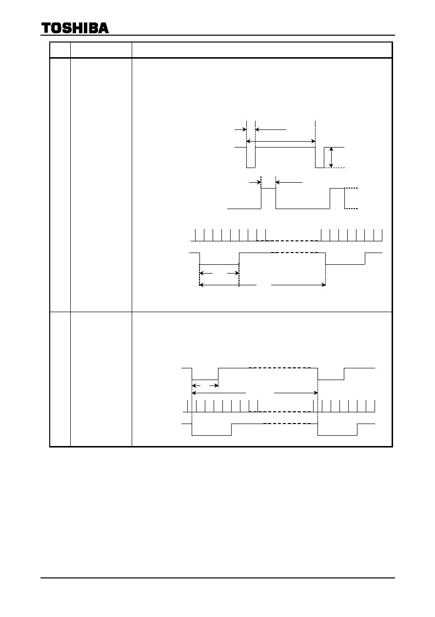
TA1316AN
2002-10-04
107
Note
No.
Parameter
Test Method
V01
VP output pulse width
Vertical free-running
(maximum pull-in
range)
(1) Input signal d (as shown in figure below) to TP16 and signal e (as shown in figure below) to
pin 24 (FBP IN).
(2) Measure VP output pulse width (VP
W
) from TP27 output waveform.
(3) Measure VP pull-in range (VP
t0
) from TP27 output waveform.
(4) Set sub-address (03) data to 01H, 02H, 03H, 04H, 05H and 06H and measure, as in step (4)
above, pull-in ranges VPt1, VPt2, VPt3, VPt4, VPt5 and VPt6.
V02
Minimum vertical
pull-in range
(1) This is same as step (1) for V01.
(2) Input signal f (as shown in figure below) to TP15.
(3) Increase signal f cycle from 30H. Measure cycle (T
VPULL
) when phase locks with that of
TP27.
Signal f (TP15
input waveform)
T
VPULL
3H
Pin 24
input waveform
TP27 waveform
Pin 24
input waveform
VPt
TP27 waveform
VPw
Signal e
(pin 24 input waveform)
9 V
GND
5.6
µs
Signal d
(TP16 input signal)
4 V
2.35
µs
29.63
µs
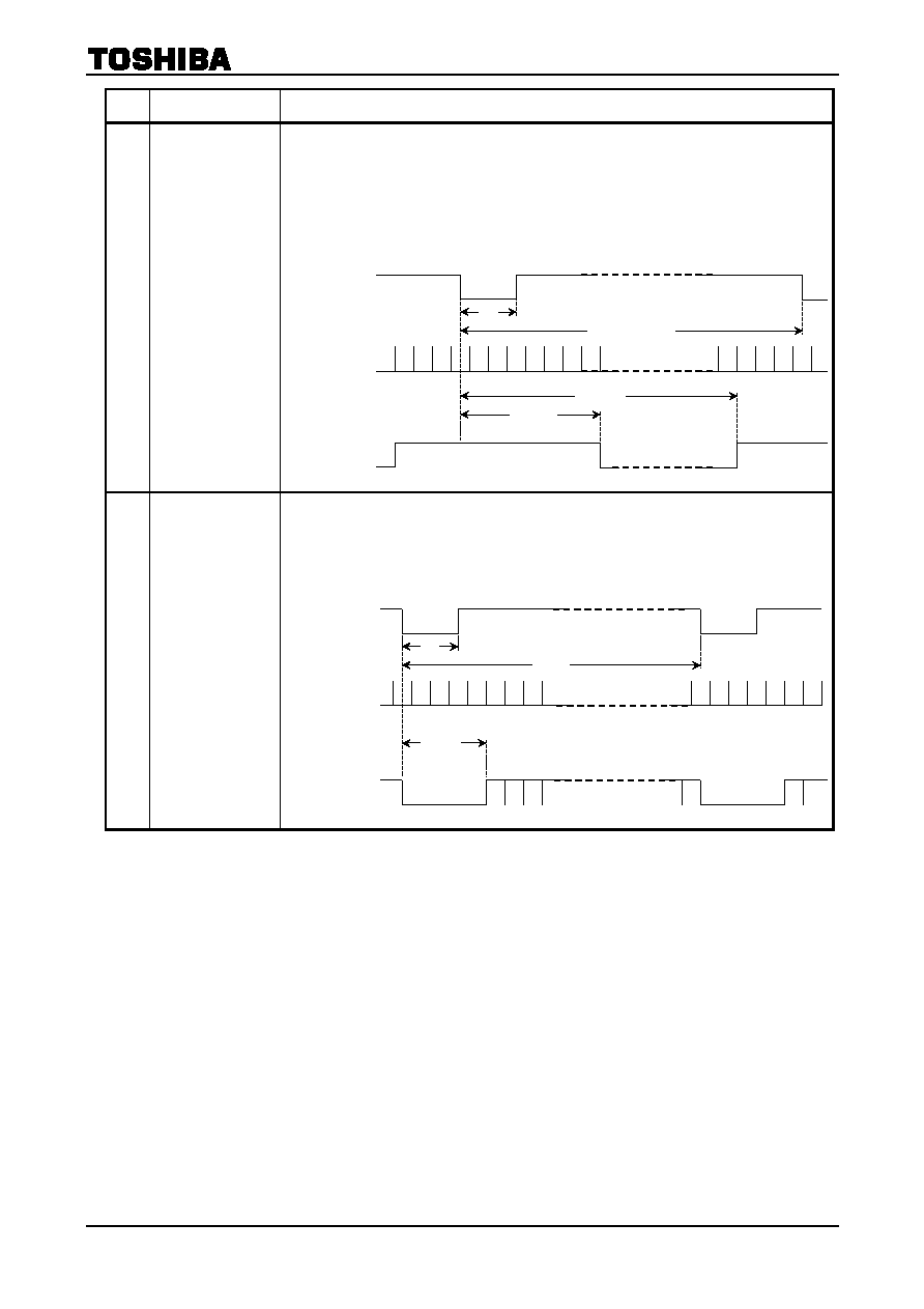
TA1316AN
2002-10-04
108
Note
No.
Parameter
Test Method
V03
Vertical black peak
detection pulse
(1) This is same as step (1) for V01.
(2) Input signal f (as shown in figure below) to TP15.
(3) Measure phase differences VBPP
0E
and VBPP
0S
from TP18 output waveform.
(4) Set sub-address (03) data to 01H, 02H, 03H, 04H, 05H and 06H, and measure as in step (3)
above, phase differences VBPP
1E
, VBPP
1S
, VBPP
2E
, VBPP
2S
, VBPP
3E
, VBPP
3S
, VBPP
4E
,
VBPP
4S
, VBPP
5E
, VBPP
5S
, VBPP
6E
and VBPP
6S
.
V04
Vertical blanking stop
phase
(1) This is same as step (1) for V01.
(2) Input signal f (as shown in figure below) to TP15.
(3) Set sub-address (03) data to 00H and F0H, and measure blanking stop phases VBLK
MIN
and
VBLK
MAX
from pin 43 output waveform.
Signal f (TP15
input waveform)
262.5H~1125H
3H
VBPP
E
VBPP
S
Pin 24
input waveform
TP18 waveform
Signal f (TP15
input waveform)
1125H
3H
Pin 24
input waveform
Pin 43 waveform
VBLK
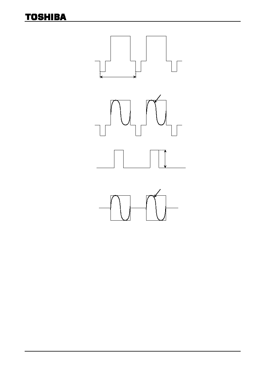
TA1316AN
2002-10-04
109
Figure T-1 Test Signals for Text/Color Difference Signal 2
Frequency f
0
sine wave
(2) Input signal 1
Amplitude A
(3) Input signal 2
(4) Input signal 3
Frequency f
0
sine wave
63.5
µs
(1) Video
signal
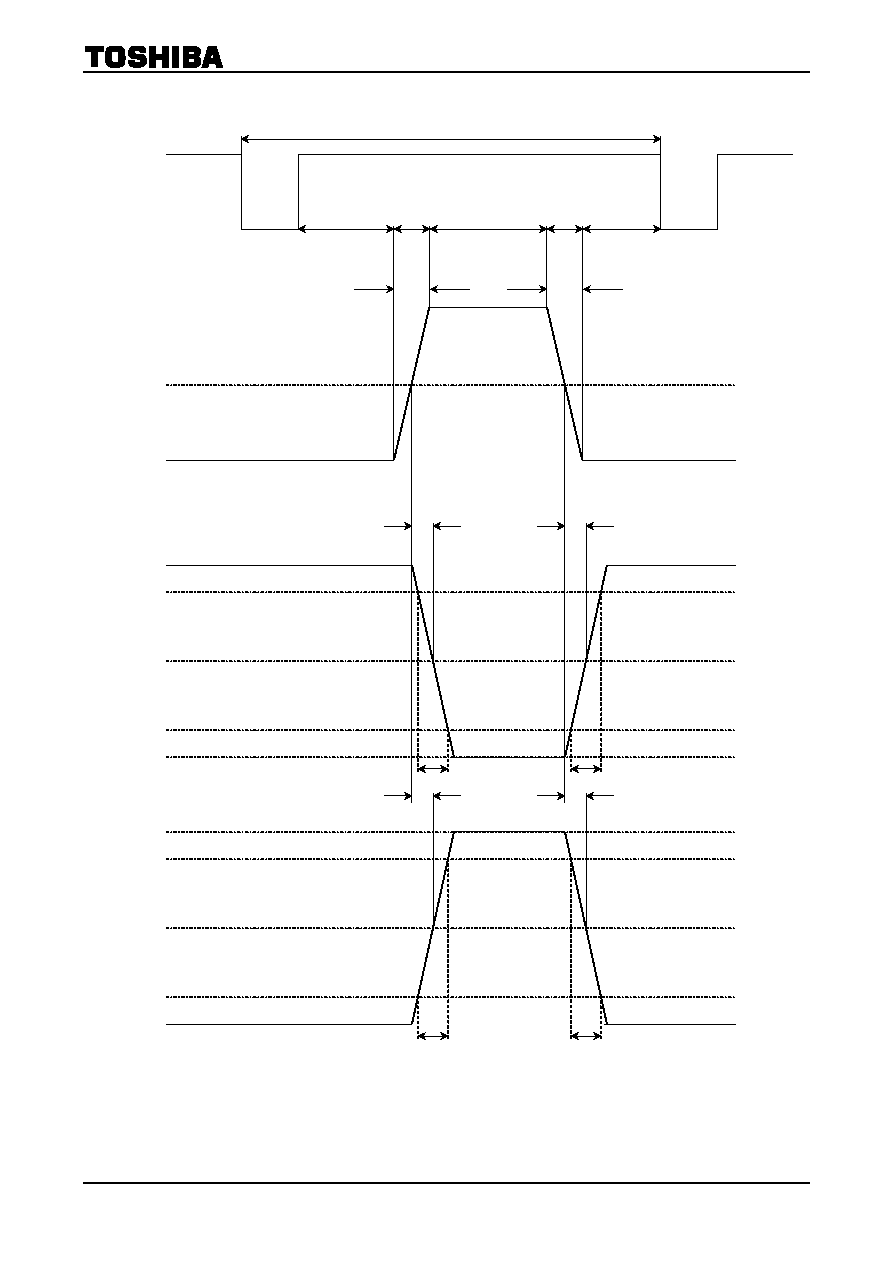
TA1316AN
2002-10-04
110
Figure T-2 Test Pulses for Text/Color Difference Signal 2
63.5
µs
20
µs
20
µs
20
µs
20 ns
20 ns
50%
0%
10%
50%
90%
t
PR
t
PF
R
F
t
PR
t
PF
R
F
0%
10%
50%
90%
100%
100%
(1) Input signal 4
(2)
(3)
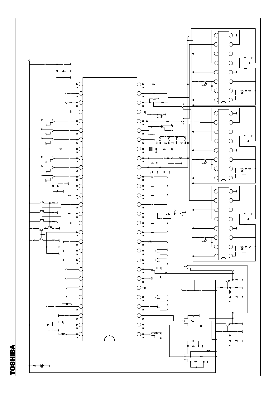
TA1316AN
2002-10-04
111
Test Circuit
A
B
C
2
k
TPD
3.
9
k
30
k
10
µ
F
0.
01
µ
F
SW
4
0.
1
µ
F
10
k
V
CC
(9 V)
#49
#50
#51
#52
APL
F
IL
T
E
R
Y/C
V
CC
VSM
O
U
T
ABC
L
IN
Y
M
/P-
M
U
T
E/BL
K
Y
S
1
(
anal
og
O
S
D)
DA
RK
A
REA
D
E
T
FILTER
BPH
F
IL
T
E
R
Y1
IN
C
b1
/P
b1
IN
C
r1
/P
r1
IN
Y
/
C
GND
MA
T
R
I
X
S
W
Y
S
2
(
anal
og
O
S
D)
Y2
IN
C
b2
/P
b2
IN
C
r2
/P
r2
IN
COLOR
LI
M
I
T
E
R
VD
2
IN
HD2
I
N
S
Y
NC I
N
VD
1
IN
HD1
I
N
SC
P
IN
SC
P
O
U
T
DE
F
/
D
A
C
V
CC
AFC
F
IL
T
E
R
HV
CO
HORI
Z
O
NT
A
L
FR
E
Q
UE
NCY
S
W
H
CURV
E
CORRE
CT
I
O
N
FBP
IN
DE
F
/
D
A
C
GND
H-OUT
VP
O
U
T
DA
C1
(S
Y
NC
OUT
)
Y
S
3
(
anal
og
RG
B
)
R
S
/
H
G
S
/
H
B
S/H
I
K
IN
RGB
GND
R
OUT
G
OUT
B O
U
T
RGB
V
CC
AN
AL
O
G
O
SD
R
IN
AN
AL
O
G
O
SD
G
I
N
AN
AL
O
G
O
SD
B
IN
DA
C2
(A
CB
pl
u
s
e
)
AN
AL
O
G
R
IN
AN
AL
O
G
G
I
N
AN
AL
O
G
B
IN
I
2
L
GND
SD
A
SC
L
I
2
L
V
DD
1
2
3
4
5
6
7
8
9
10
11
12
13
14
15
16
17
18
19
20
21
22
23
24
25
26
27
28
56
55
54
53
52
51
50
49
48
47
46
45
44
43
42
41
40
39
38
37
36
35
34
33
32
31
30
29
TA1316AN
0.
1
µ
F
0.
01
µ
F
2.
0
V
#56
#40
10
k
100
µ
F
0.
01
µ
F
#54
#53
SW
5
6
SW
5
4
3
k
100
k
TP31
100
#48
0.
1
µ
F
#47
0.
1
µ
F
#46
#45
10
k
10
k
6.
8
V
300
pF
#43
100
10
k
#42
100
10
k
#41
100
10
k
0.
1
µ
F
#39
TP39
SW
3
9
A
B
0.
1
µ
F
#38
TP38
SW
3
8
A
B
0.
1
µ
F
#37
TP37
SW
3
7
A
B
#36
470
9 V
0.
1
µ
F
#35
TP35
SW
3
5
A
B
0.
1
µ
F
#34
TP34
SW
3
4
A
B
0.
1
µ
F
#33
TP33
SW
3
3
A
B
#31
470
#30
TP30
1/
2
W
240
#29
0.
1
µ
F
100
µ
F
#55
1
µ
F
0.
01
µ
F
470
LED
#1
SW
2
#2
#3
#4
SW
1
TP1
TP4
A
B
A
B
#5
TP5
SW
5
A
B
#7
SW
7
A
B
#8
SW
8
A
B
0.
1
µ
F
0.
1
µ
F
0.
1
µ
F
#9
SW
9
A
B
0.
1
µ
F #10
SW
1
0
A
B
0.
1
µ
F
TP9
TP10
#11
TP12
#12
100
TP13
#13
100
TP15
#15
100
TP16
#16
100
TP17
#17
100
TP18
#18
1
k
TP27
#27
30
k
#28
#14
TP14a
1
µ
F N
P
TP14b
A
B
SW
2
0
#20
TP20
1
k
3
k
10
µ
F
1
µ
F
0.
01
µ
F
#21
TP21
C
SBL
A5
0
3
KEC
Z
F
3
0
470
#22
33
k
56
k
2
k
5.
1
k
75
TPC
TPB
3.
9
k
2
k
5.
1
k
75
TPA
10
µF
10
µF
A
B
S
W
I
NP
UT
SW
3
0.
1
µ
F
20
k
100
k
A
B
C
1
µ
F
20
k
30
pF
1
µ
F
#23
SW
2
3
A
B
TP23b
1
µ
F
TP23a
100
10
k
#24
3.
9
k
#26
10
k
S
W
24b
V
CC
(9 V)
5.
1
k
16
15
14
13
12
11
10
9
1
2
3
4
5
6
7
8
TC4538BP
1200 pF
50
k
7.
5
k
1000 pF
5.
1
k
50
k
51
k
51
k
16
15
14
13
12
11
10
9
1
2
3
4
5
6
7
8
TC4538BP
1200 pF
50
k
7.
5
k
1000 pF
5.
1
k
50
k
51
k
51
k
16
15
14
13
12
11
10
9
1
2
3
4
5
6
7
8
TC4538BP
1200 pF
50
k
7.
5
k
1000 pF
5.
1
k
50
k
51
k
51
k
S
W
24A
SW
2
6
A
C
B
A
C
B
15.75 kHz
31.5/33.75 kHz
45 kHz
10
µ
F
10
µ
F
10
µ
F
2.
2
µ
F
100
µ
F
10
k
0.
1
µ
F
15
k
15
k
15
k
SW14
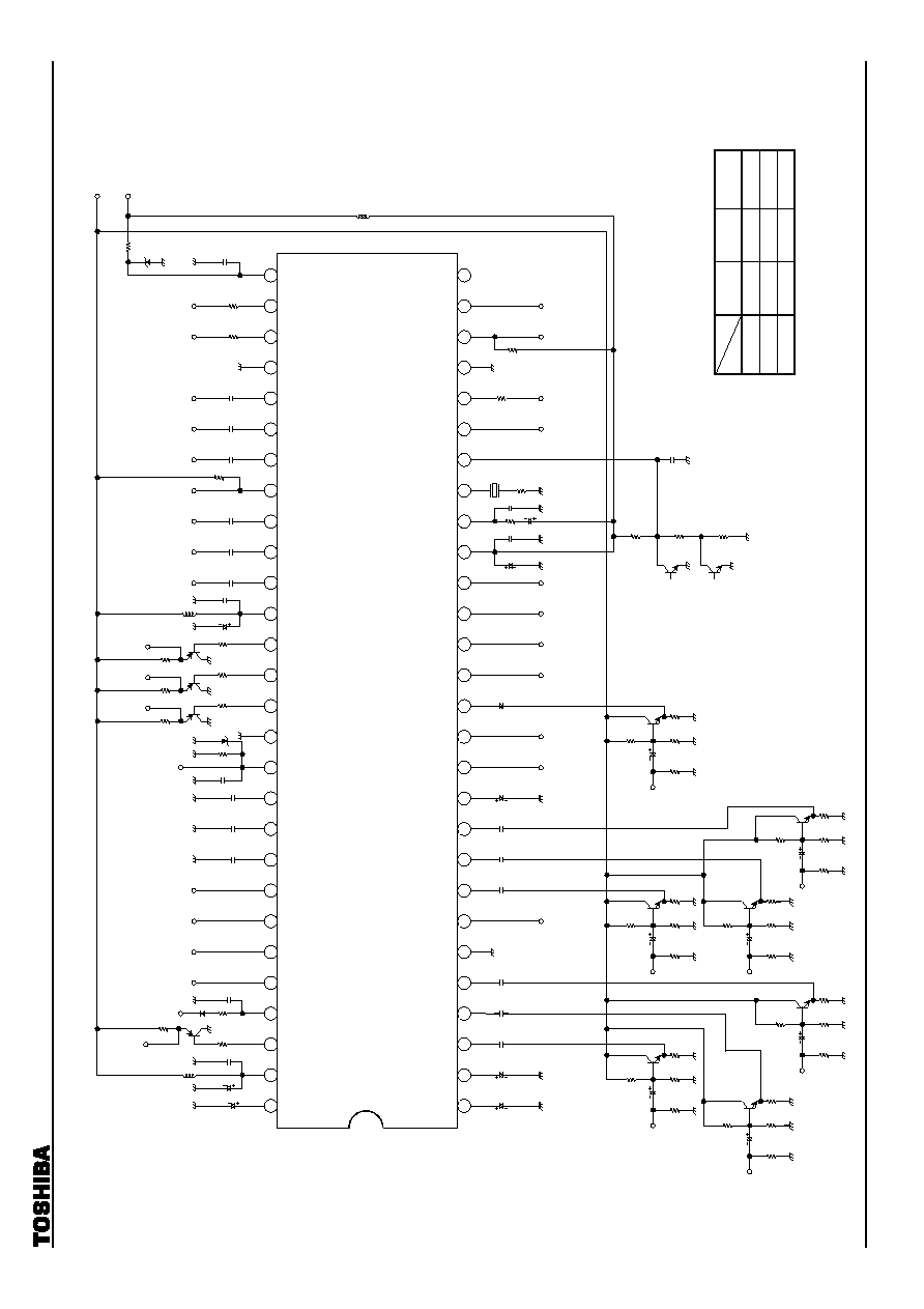
TA1316AN
2002-10-04
112
Application Circuit
M
M
M
: Mylar capacitor
M
M
M
M
M
10
k
100
k
470
C
SBL
A5
0
3
KEC
Z
F
3
0
470
V
CC
M
a
tr
ix
S
W
SCL
VD
2
-
IN
HD2-I
N
VD
1
-
IN
HD1-I
N
SC
P-
IN
SC
P-
O
U
T
CURV
E
COR
R
FBP-
IN
H-OUT
VP-
O
U
T
SDA
V
CC
AN
AL
O
G
B-
I
N
AN
AL
O
G
G
-
I
N
AN
AL
O
G
R
-
I
N
DA
C2-OUT
OS
D
B
-
I
N
OS
D
G-I
N
OS
D
R-I
N
B-
OU
T
G-OUT
R-OUT
Ys3
Ys2
Ys1
YM
ABC
L
VSM
-
O
U
T
APL
F
IL
T
E
R
Y/C
V
CC
VSM
O
U
T
ABC
L
IN
Y
M
/P-
M
U
T
E/BL
K
Y
S
1
(
anal
og
O
S
D)
DA
RK
A
REA
D
E
T
FILTER
BPH
F
IL
T
E
R
Y1
IN
C
b1
/P
b1
IN
C
r1
/P
r1
IN
Y
/
C
GND
MA
T
R
I
X
S
W
Y
S
2
(
anal
og
O
S
D)
Y2
IN
C
b2
/P
b2
IN
C
r2
/P
r2
IN
COLOR
LI
M
I
T
E
R
VD
2
IN
HD2
I
N
S
Y
NC I
N
VD
1
IN
HD1
I
N
SC
P
IN
SC
P
O
U
T
DE
F
/
D
A
C
V
CC
AFC
F
IL
T
E
R
HV
CO
HORI
Z
O
NT
A
L
FR
E
Q
UE
NCY
S
W
H
CURV
E
CORRE
CT
I
O
N
FBP
IN
DE
F
/
D
A
C
GND
H-OUT
VP
O
U
T
Y
S
3
(
anal
og
RG
B
)
R
S
/
H
G
S
/
H
B
S/H
I
K
IN
RGB
GND
R
OUT
G
OUT
B O
U
T
RGB
V
CC
AN
AL
O
G
O
SD
R
IN
AN
AL
O
G
O
SD
G
I
N
AN
AL
O
G
O
SD
B
IN
DA
C2
(A
CB
pl
u
s
e
)
AN
AL
O
G
R
IN
AN
AL
O
G
G
I
N
AN
AL
O
G
B
IN
I
2
L
GND
SD
A
SC
L
I
2
L
V
DD
1
2
3
4
5
6
7
8
9
10
11
12
13
14
15
16
17
18
19
20
21
22
23
24
25
26
27
28
56
55
54
53
52
51
50
49
48
47
46
45
44
43
42
41
40
39
38
37
36
35
34
33
32
31
30
29
TA1316AN
0.
1
µ
F
0.
1
µ
F
1
µ
F
0.
1
µ
F
1
µ
F
0.
1
µ
F
0.
1
µ
F
0.
1
µ
F
1
µ
F
2.
2
µ
F
1
k
3.
9
k
5.
1
k
75
Y2-IN
Y1-IN
Cb/
Pb2-IN
Cr/Pr2-IN
Cr/Pr1-IN
Cb/Pb1-IN
1
k
75
1
k
10
µF
75
1
k
3.
9
k
5.
1
k
75
10
µF
10
µF
10
µF
1
k
10
µF
75
1
k
10
µF
75
1
k
3.
9
k
5.
1
k
75
SYNC-IN 10
µF
3
k
100
µ
F
0.
01
µ
F
1
µ
F
1
k
470
0.
01
µ
F
0.
1
µ
F
0.
1
µ
F
0.
1
µ
F
0.
1
µ
F
0.
1
µ
F
0.
1
µ
F
0.
01
µ
F
0.
01
µ
F
0.
01
µ
F
2.
2
µ
F
100
µ
F
0.
01
µ
F
0.
01
µ
F
30
k
0.
01
µ
F
100
100
IK
I
N
2.
0
V
30
k
300
pF
100
µ
F
0.
01
µ
F
6.
8
V
100
47
µ
H
47
µ
H
47
µ
H
1
k
A
560
B
1.
5
k
0.
1
µ
F
Application of H-FREQ switching (31.5 k/33.75 k/45 kHz)
Tr.
H-FREQ
A
B
Pin 22
Voltage
31.5 kHz
L
L
6 V
33.75 kHz
L
H
3 V
45 kHz
H
*
0 V
*: Don't care
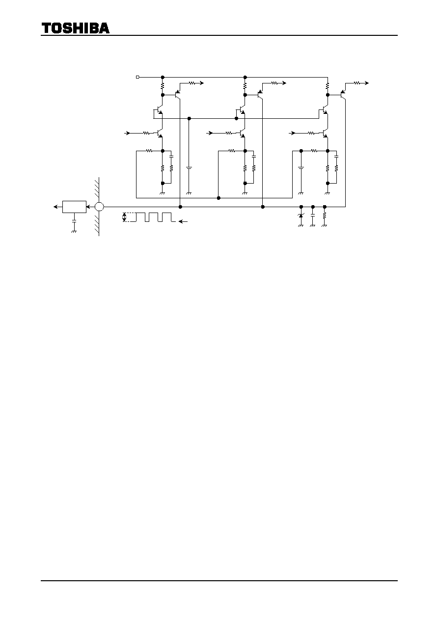
TA1316AN
2002-10-04
113
ACB Application Circuit
45
CRT
B
CRT
G
CRT
R
20~51
k
51~330
pF
6.
8
V
Z
+B
R
G
B
1 V
p-p
0~3.0 V (DC)
CLAMP
I
K
IN
TA1316AN
2002-10-04
114
Package Dimensions
Weight: 5.55 g (typ.)

TA1316AN
2002-10-04
115
∑ TOSHIBA is continually working to improve the quality and reliability of its products. Nevertheless, semiconductor
devices in general can malfunction or fail due to their inherent electrical sensitivity and vulnerability to physical
stress. It is the responsibility of the buyer, when utilizing TOSHIBA products, to comply with the standards of
safety in making a safe design for the entire system, and to avoid situations in which a malfunction or failure of
such TOSHIBA products could cause loss of human life, bodily injury or damage to property.
In developing your designs, please ensure that TOSHIBA products are used within specified operating ranges as
set forth in the most recent TOSHIBA products specifications. Also, please keep in mind the precautions and
conditions set forth in the "Handling Guide for Semiconductor Devices," or "TOSHIBA Semiconductor Reliability
Handbook" etc..
∑ The TOSHIBA products listed in this document are intended for usage in general electronics applications
(computer, personal equipment, office equipment, measuring equipment, industrial robotics, domestic appliances,
etc.). These TOSHIBA products are neither intended nor warranted for usage in equipment that requires
extraordinarily high quality and/or reliability or a malfunction or failure of which may cause loss of human life or
bodily injury ("Unintended Usage"). Unintended Usage include atomic energy control instruments, airplane or
spaceship instruments, transportation instruments, traffic signal instruments, combustion control instruments,
medical instruments, all types of safety devices, etc.. Unintended Usage of TOSHIBA products listed in this
document shall be made at the customer's own risk.
∑ The products described in this document are subject to the foreign exchange and foreign trade laws.
∑ The information contained herein is presented only as a guide for the applications of our products. No
responsibility is assumed by TOSHIBA CORPORATION for any infringements of intellectual property or other
rights of the third parties which may result from its use. No license is granted by implication or otherwise under
any intellectual property or other rights of TOSHIBA CORPORATION or others.
∑ The information contained herein is subject to change without notice.
000707EBA
RESTRICTIONS ON PRODUCT USE