 | –≠–ª–µ–∫—Ç—Ä–æ–Ω–Ω—ã–π –∫–æ–º–ø–æ–Ω–µ–Ω—Ç: TA1343N | –°–∫–∞—á–∞—Ç—å:  PDF PDF  ZIP ZIP |
TA1343N
2002-02-12
1
TOSHIBA Bipolar Linear IC Silicon Monolithic
TA1343N
TV Sound Processor
TA1343N is a sound processor controlled by I
2
C bus. It
incorporates the following: 2-channel input, 3-channel output
signal processing circuit, phase shift circuit for surround, and
LPF for woofer channel.
ALS (Automatic Level Suppresser) circuit which prevents
distort the signal in large signal condition for woofer channel is
also incorporated
Features
∑ Sound processing circuit
∑ 2 ch inputs (Lch, Rch)
∑ 3 ch outputs (Lch, Rch, Wch)
∑ Input matrix switch
∑ Volume control
∑ Bass, treble, and balance adjustment
∑ Woofer level and surround effect level adjustment
∑ ALS (automatic level suppresser) circuit
∑ Built-in LPF for bass boost
∑ Surround circuit
∑ Phase shift surround system
∑ 2 modes stereo surround
∑ Pseudo stereo mode
Weight: 1.22 g (typ.)
TA1343N
2002-02-12
2
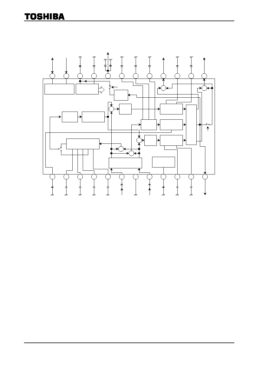
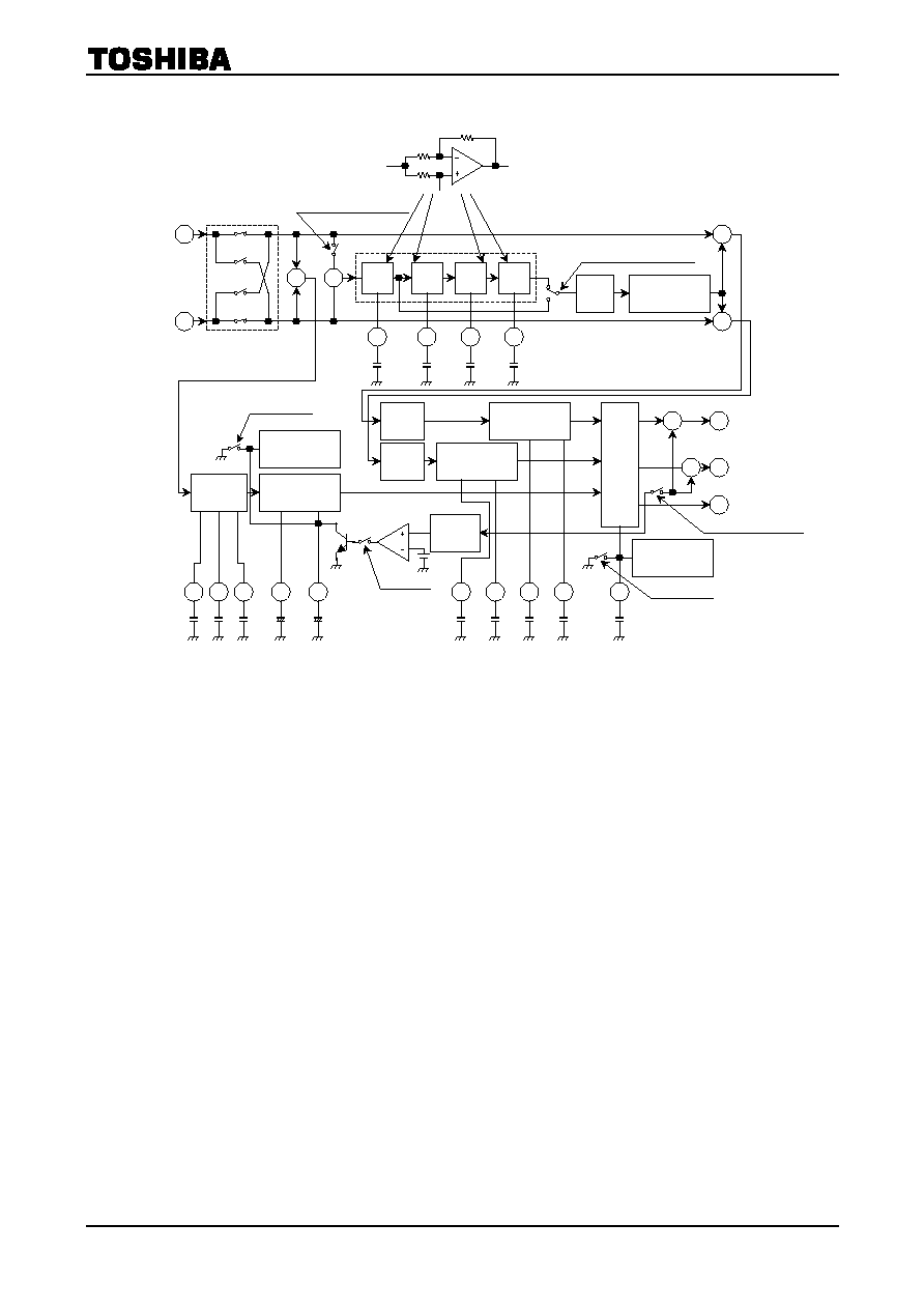
Block Diagram
+
-
I
2
C bus
interfaxe
0dB
/
-
5dB
Phase sifter
Input matrix
Bias
Reg.
12
9
14
15
16
17
18
19
20
21
22
23
24
+
+
Ba
s
s
b
o
o
st
SW
4
f
f
Bia
s
Fil
t
e
r
10
Ba
s
s
L
P
F (
R
)
11
Trebl
e HP
F
(R)
Wc
h Ou
t
p
u
t
13
Trebl
e HP
F
(L)
Rc
h Out
p
u
t
Lc
h Ou
t
put
Ba
s
s
L
P
F (
L
)
SD
A
SC
L
Woof
er Fi
l
t
e
r
Vo
lu
me
Fil
t
e
r
Woof
er LP
F2
Woof
er LP
F3
Woof
er LP
F1
V
CC
(9 V
)
8
5
B
1
6
Lc
h I
npu
t
7
GND
Rc
h I
npu
t
4
1
O.
C.
2
B
4
3
B
3
B
2
0dB
/
-
5dB
-
+
L.P.F
L-R Level
Control
Level
Control
DAC
AGC
Det
L.P.F
V
o
l
u
m
e
&
B
al
an
c
e
Cont
rol
Bass&
Treble
Control
Bass&
Treble
Control
Woofer
Level
Control
ALS SW
TA1343N
2002-02-12
3
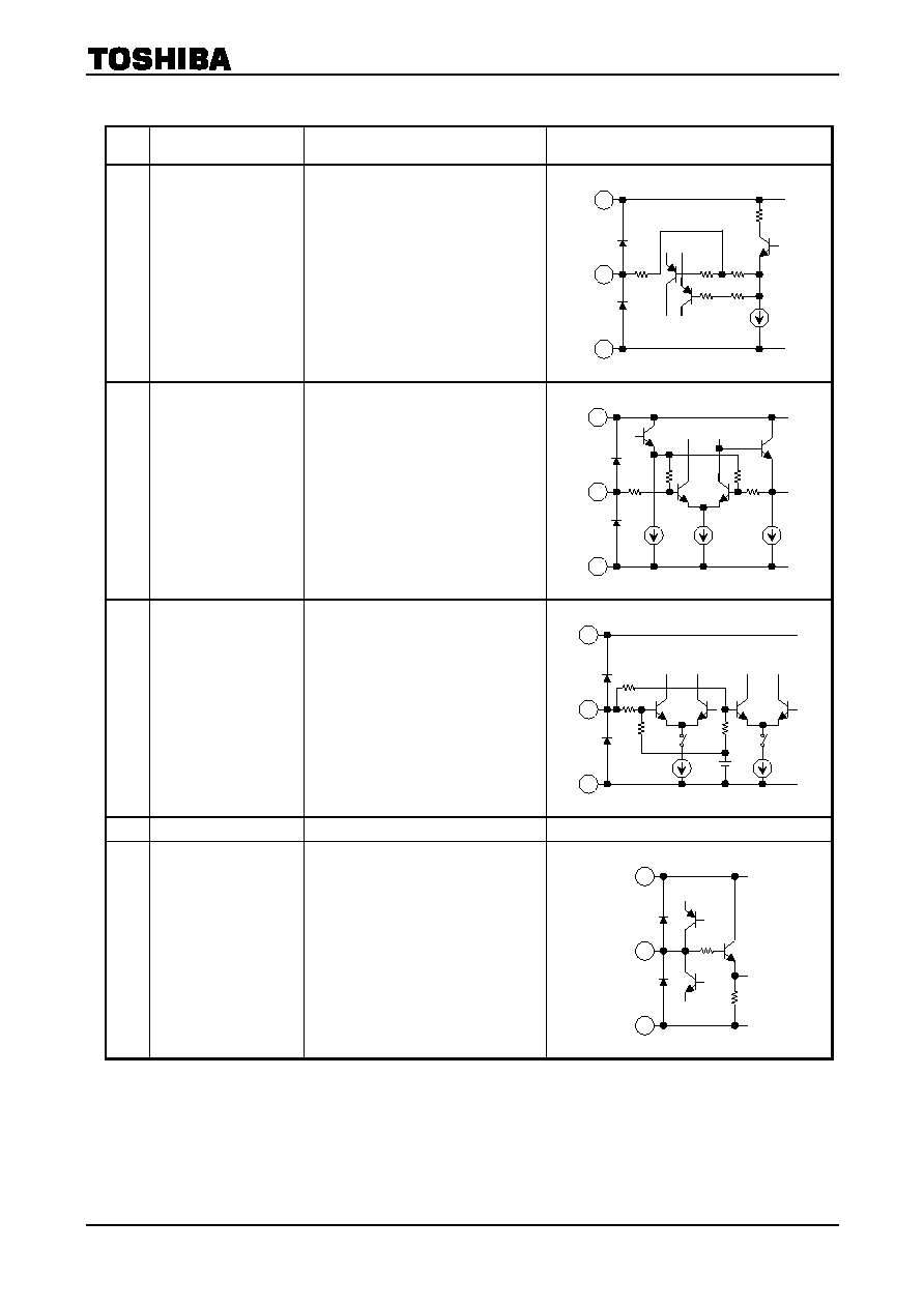
Terminal Function
Pin
No.
Name Function
Interface
Circuit
1 Offset
canceling
filter
DC offset canceling filter for bass boost.
Connect a capacitor (10
m
F) between this
terminal and GND.
2
3
4
5
f
4
f
3
f
2
f
1
Terminals for capacitors of the phase shift
blocks.
Value of phase shift each block is
f
deg.
=
-
2tan
-
1
(2
p
fCR)
C is capacitance of external
capacitor
R is resistance of internal resister
(10 k
W
(typ.)).
6
8
Lch Input
Rch Input
Audio input terminals.
7 GND
GND
terminals.
9 Bias
Filter
Filter for noise rejection of the bias.
Connect a capacitor (4.7
m
F) between this
terminal and GND.
1 k
9
30 k
W
100
W
7
20
1
10 k
9
100
W
7
20
2
3
4
5
56 k
9
24 k
W
7
20
6
8
24 k
W
56 k
9
4.
5 V
7
20
9

TA1343N
2002-02-12
4
Pin
No.
Name Function
Interface
Circuit
10
15
Bass LPF (R)
Bass LPF (L)
LPFs for bass control circuits.
Connect capacitors (0.027
m
F) between
each terminals and GND.
11
14
Treble HPF (R)
Treble HPF (L)
HPFs for treble control circuits.
Connect capacitors (8200 pF) between
each terminals and GND.
12
13
16
Wch Output
Rch Output
Lch Output
Audio output terminal.
17
18
19
Woofer LPF 1
Woofer LPF 2
Woofer LPF 3
LPFs for bass boost circuit.
Connect a capacitor (0.033
m
F) between
terminal 17 and GND.
Connect a capacitor (0.047
m
F) between
terminal 18 and GND.
Connect a capacitor (0.022
m
F) between
terminal 19 and GND.
20 V
CC
V
CC
terminal.
Recommended operation voltage is 9 V
±
10%.
22 k
9
100
W
7
20
10
15
22 k
W
4.
5 V
4.
5 V
22 k
W
11 k
W
7
20
11
14
22 k
9
100
W
7
20
12
13
16
100
9
1 m
A
7
20
17
18
19
2 k
W

TA1343N
2002-02-12
5
Pin
No.
Name Function
Interface
Circuit
21 Volume
Filter
Smoothing filter for volume control.
Connect a capacitor (0.01
m
F) between
this terminal and GND.
22 Woofer
Filter
Smoothing filter for bass boost level
control.
Connect a capacitor (3.3
m
F) between this
terminal and GND.
This filter is also for ALS circuit.
23 SCL
SCL
terminal.
24 SDA
SDA
terminal.
7
20
I
2
C Bus
Control
21
7
20
23
2.
3 V
2.
3 V
7
20
24
7
20
22
I
2
C Bus
Control
TA1343N
2002-02-12
6
I
2
C Bus Control Data Table
Slave Address: 80 (h)
Address Map
Sub
Address
MSB (b7)
b6 b5 b4 b3 b2 b1
LSB
(b0)
Default
Data
00
Bass level (effective data range: 0E (h) to 72 (h))
40 (h) (Bass: Center)
01
Treble level (effective data range: 0E (h) to 72 (h))
40 (h) (Treble: Center)
02
Volume (effective data range: 00 (h) to 72 (h))
00 (h) (Volume: min)
03
ALS SW
"0": OFF
"1": ON
ALS
start point
"00": 220 mV
"01": 380 mV
"10": 525 mV
"11": 770 mV
Input
attenuati
on
"0": 0dB
"1":
-
5dB
Input matrix
"00": Normal
"01": Rch
"10": Lch
"11": Reverse
00 (h)
(ALS SW: OFF
ALS start point:
220 mV
Input attenuation: 0dB
Input matrix: Normal)
04
Woofer level (effective data range: 00 (h) to 72 (h))
00 (h) (Woofer level: min)
05
Balance (effective data range: 00 (h) to 7F (h))
40 (h) (Balance: Center)
06
Surround
mode 2
"0":
Ste.
"1":
Mono.
Surround
mode 1
"0":
f
"1": 4
f
Surround effect level
(effective data range 1 (h) to 7
(h))
0 (h): OFF
C0 (h)
(Surround mode 1: 4
f
Surround mode 2:
Mono.
Surround effect level: OFF)
07
Bass
boost
SW
"0": OFF
"1": ON
Woofer LPF fo
"00": 100 Hz
"01": 125 Hz
"10": 170 Hz
"11": 210 Hz
Woofer
LPF
defeat
"0": OFF
"1": ON
Muting 2
"0": OFF
"1": ON
Muting 1
"0": OFF
"1": ON
10 (h)
Bass boost SW: OFF
Woofer LPF fo: 125 Hz
Muting 1: OFF
Muting 2: OFF
The bits shown gray area must be "0".
TA1343N
2002-02-12
7
Block Diagram
Lch Input 6
8
Rch Input
2
B
4
3
B
3
4
B
2
5
B
1
+
LPF
0dB
/
-
5dB
0dB
/
-
5dB
Vo
lu
me
&Ba
l
a
n
ce
Cont
rol
ALS SW
Bass boost SW
Level
Control
DAC
1
O.
C.
22
Woof
er Fi
l
t
e
r
17
Woof
er LP
F1
18
Woof
er LP
F2
19
Woof
er LP
F3
10
Ba
s
s
L
P
F (
R
)
11
Trebl
e HP
F
(R)
15
Ba
s
s
L
P
F (
L
)
14
Trebl
e HP
F
(L)
21
Vo
lu
me
Fil
t
e
r
Muting 1
Bass
Treble
Control
Bass
Treble
Control
+
+
16 Lch Output
13 Rch Output
12 Wch Output
Woofer
Level
Control
AGC
Det
Level
Control
DAC
Muting 2
L.P.F
-
L-R Level
Control
-
+
Surround mode 1
Surround mode 2
Phase
Sifter
Input matrix
4
f
10 k
W
f
The on/off status of each switches drawn on this scheme shows
the default setting of I
2
C bus control.

TA1343N
2002-02-12
8
Explanation of the Functions.
(note: (h) means hexadecimal data, (b) means binary data)
∑ Bass level control (sub address 00 (h))
Bass level control. Crossover frequency is 1 kHz.
Effective control data range is 0E (h) to 72 (h) (100 steps). Set this data to 0E (h), bass level goes to
minimum level, and set this data to 72 (h), bass level goes to maximum level. Set this data to 40 (h), bass
level goes to center level.
Switch on default data is 40 (h).
Control range is ±12dB (typ.).
∑ Treble level control (sub address 01 (h))
Treble level control. Crossover frequency is 1 kHz.
Effective control data range is 0E (h) to 72 (h) (100 steps). Set this data to 0E (h), treble level goes to
minimum level, and set this data to 72 (h), treble level goes to maximum level. Set this data to 40 (h),
treble level goes to center level.
Switch on default data is 40 (h).
Control range is ±12dB (typ.).
∑ Volume control (sub address 02 (h))
Volume control of only Lch and Rch output.
Effective control data range is 00 (h) to 72 (h).
Switch on default data is 00 (h).
∑ Woofer level control (sub address 04 (h))
Volume control of only Wch output.
Effective control data range is 00 (h) to 72 (h).
Switch on default data is 00 (h).
∑ Balance control (sub address 05 (h))
Balance control. Set this data to 40 (h), balance goes to center.
Effective control data range is 00 (h) to 7F (h).
Switch on default data is 40 (h).
∑ Surround effect level control (sub address 06 (h)/b2 to b0)
Surround effect level control.
Effective control data range is 1 (h) to 7 (h). Set this data to 0 (h), surround function is off. Recommend
setting surround 2 data to 1 (b) when surround effect level set to "0".
Set mute on when surround effect level is changed.
Switch on default data is 0 (h).
∑ Input matrix switch (sub address 03 (h)/b1 to b0)
Output signal selection control.
Set these bits to 00 (b), output mode goes to normal mode (input signal of terminal 6 is outputted to
terminal 16, and input signal of terminal 8 is outputted to terminal 13). Set these bits to 01 (b) output
mode goes to Rch mode (input signal of terminal 8 is outputted to terminal 13 and terminal 16). Set these
bits to 10 (b) output mode goes to Lch mode (input signal of terminal 6 is outputted to terminal 13 and
terminal 16). Set these bits to 11 (b), output mode goes to reverse mode (input signal of terminal 6 is
outputted to terminal 13, and input signal of terminal 8 is outputted to terminal 16).
Switch on default data is 00 (b).
∑ Input attenuation (sub address 03 (h)/b2)
When this function is active, input signals are -5dB attenuated at input stage of Lch and Rch. Wch
signal isn't attenuated.
So, Wch output signal level is up to 5dB from Lch and Rch outputs relatively.
Set the bit to 0 (b), attenuation is inactive, set the bit to 1 (b), attenuation is active.
Switch on default data is 0 (b).

TA1343N
2002-02-12
9
∑ ALS switch (sub address 03 (h)/b6), ALS start point (sub address 03 (h)/b5 to b4)
Gain of Wch is large. So output signals of Wch is distort easily when the input signals are large. ALS
(Automatic Level Suppresser) suppresses Wch signal level under ALS start point, and reduces the
distortion in large signals input condition.
Set the bit of sub address 03 (h)/b6 to 0 (b), ALS is inactive. Set the bit 1 to (b), ALS is active.
Switch on default data is 0 (b).
The bits of 03 (h)/b5 to b4 set ALS start point. Set the bits to 00 (b), ALS start point is 220 mV
rms
. Set
the bits to 01 (b), ALS start point is 380 mV
rms
. Set the bits to 10 (b), ALS start point is 525 mV
rms
. And
set the bits to 11 (b), ALS start point is 770 mV
rms
.
Switch on default data is 00 (b).
∑ Surround mode 1 (sub address 06 (h)/b6), Surround mode 2 (sub address 06 (h)/b7)
Surround mode 1 is selection of phase shift value of the surround circuit. Set the bit to 0 (b), L-R signal is
shifted by 1 phase shift stage. Set the bit to 1 (b), L-R signal is shifted by 4 phase shift stages.
Surround mode 2 is selected by condition of the input signal. When input signal is stereo, surround mode
2 must be set to 0 (b). When input signal is monaural, surround mode 2 must be set to 1 (b) (pseudo stereo
mode).
Recommend setting surround 1 to 1 (b) when pseudo stereo mode is selected.
∑ Mute 1 (sub address 07 (h)/b0), Mute 2 (sub address 07 (h)/b1)
When Mute 1 is active, all outputs are muted.
Set the bit to 0 (b), mute 1 is inactive. Set the bit to 1 (b), Mute 1 is active.
Switch on default data is 0 (b).
When Mute 2 is active, only Wch output is muted. Set the bit to 0 (b), Mute 2 is inactive. Set the bit to 1
(b), Mute 2 is active.
Switch on default data is 0 (b).
∑ Woofer LPF fo (sub address 07 (h)/b5 to b4)
These bits set cut off frequency (fo) of the low pass filter for Wch.
Set the bits to 00 (b), fo is 100 Hz (-3dB point). Set the bits to 01 (b), fo is 125 Hz. Set the bits to 10 (b), fo
is 170 Hz. Set the bits to 11 (b), fo is 210 Hz.
Switch on default data is 01 (h).
∑ Woofer LPF defeat (sub address 07 (h)/b3)
Set the bit to 1 (b), Woofer LPF is defeated.
This function is for device test. So, this bit must be set to 0 (b).
Switch on default data is 0 (b).
∑ Bass boost switch (sub address 07 (h)/b7)
Bass boost function is adding Wch signal to main channel signals. It can boost low frequency signal
without woofer output.
Set the bit 0 (b), Bass boost is inactive. Set the bit 1 (b), bass boost is active.
Switch on default data is 0 (b).
Purchase of TOSHIBA I
2
C components conveys a license under the Philips I
2
C Patent Rights to use
these components in an I
2
C system, provided that the system conforms to the I
2
C Standard Specification
as define by Philips.
TA1343N
2002-02-12
10
Maximum Ratings
(Ta
=
=
=
=
25∞C)
Characteristics Symbol Rating Unit
Supply voltage
V
CC
12 V
Power dissipation
P
D
1400
(Note
1)
mW
Operating temperature
T
opr
-
20 to 75
∞C
Storage temperature
T
stg
-
55 to 150
∞C
Maximum input voltage
V
MAX
V
CC
+
0.3
V
Minimum input voltage
V
MIN
V
CC
-
0.3
V
Note 1: When using the device at Ta
=
25∞C, decrease the power dissipation by 11.2 mW for each increase of 1∞C
Recommended Supply Voltage
Pin No.
Pin Name
Min
Typ.
Max
Unit
20 V
CC
8.1
9.0
9.9
V
Electrical Characteristics
DC Characteristics
(V
CC
=
=
=
=
9 V, Ta
=
=
=
=
25∞C)
Characteristics
Pin
No.
Pin Name
Symbol
Test
Circuit
Test Condition
Min
Typ.
Max
Unit
Power
dissipation
20 V
CC
I
CC
39 50 63 mA
1
Offset canceling
filter
V1
4.0 4.5 5.0
2
f
4
V2
4.0 4.5 5.0
3
f
3
V3
4.0 4.5 5.0
4
f
2
V4
4.0 4.5 5.0
5
f
1
V5
4.0 4.5 5.0
6
Lch
Input
V6
4.0 4.5 5.0
8
Rch
Input
V8
4.0 4.5 5.0
9
Bias
Filter
V9
5.2 5.7 6.2
10
Bass
LPF
(R)
V10
4.0 4.5 5.0
11
Treble LPF (R)
V11
4.0
4.5
5.0
12
Wch
Output
V12
4.0 4.5 5.0
13
Rch
Output
V13
4.0 4.5 5.0
14
Treble LPF (L)
V14
4.0
4.5
5.0
15
Bass
LPF
(L)
V15
4.0 4.5 5.0
16
Lch
Output
V16
4.0 4.5 5.0
17
Woofer
LPF1
V17
4.6 5.1 5.6
18
Woofer
LPF2
V18
4.6 5.1 5.6
19
Woofer
LPF3
V19
4.6 5.1 5.6
21 Volume
Filter
V21
æ
0.0
æ
Pin voltage
22 Woofer
Filter
V22
1
In power on default
0.5 1.5 2.0
V
TA1343N
2002-02-12
11
AC Characteristics
(V
CC
=
=
=
=
9 V, Ta
=
=
=
=
25∞C)
Characteristics Symbol
Test
Circuit
Test Condition
Min
Typ.
Max
Unit
Go L
æ
Go R
æ
0.0 2.0 4.0
Go
Att
L
æ
Go
Att
R
æ
-
7.0
-
5.0
-
3.0
Go
Bst
L
æ
Go
Bst
R
æ
11.0 13.0 15.0
Gain
Go W
æ
(Note 1)
16.0 19.0 22.0
dB
THD L
æ
THD R
æ
0.03
THD
THD W
æ
(Note 2)
æ
0.25
1.0 %
SN L
æ
SN R
æ
70 74
S/N
SN W
æ
(Note 3)
68 72
æ
dB
v
NO
L
æ
v
NO
R
æ
Residual noise
v
NO
W
æ
(Note 4)
æ
20 50
µV
rms
Go100 L
æ
Frequency response (100 Hz)
Go100 R
æ
(Note 5)
-
2.0 0.0 2.0 dB
Go10k L
æ
Go10k R
æ
-
2.0 0.0 2.0
Frequency response (10 kHz)
Go10k S
æ
(Note 6)
-
13.0
-
11.0
-
8.0
dB
G
LPF
100
æ
4.0 6.0 8.0
G
LPF
125
æ
5.5 7.5 9.5
G
LPF
170
æ
4.0 6.0 8.0
LPF frequency response
G
LPF
210
æ
(Note 7)
1.0 8.0 15.0
dB
Surround sound gain
G S
æ
(Note
8)
1.5 3.5 5.5 dB
Surround sound phase
Ph 4
f
æ
(Note 9)
-
65
-
110
-
65
deg.
Balance center
D
G
LR
æ
(Note 10)
-
2.0 0.0 2.0 dB
G
BLMIN
L
æ
Balance minimum
G
BLMIN
R
æ
(Note 11)
æ
-
70
-
60
dB
G
BSMAX
L
æ
Bass maximum
G
BSMAX
R
æ
(Note 12)
9
12
14
dB
G
BSMIN
L
æ
Bass minimum
G
BSMIN
R
æ
(Note 13)
-
14
-
12
-
9 dB
G
TRMAX
L
æ
Treble maximum
G
TRMAX
R
æ
(Note 14)
9
12
14
dB
G
TRMIN
L
æ
Treble minimum
G
TRMIN
R
æ
(Note 15)
-
14
-
12
-
9 dB
G
VLCNT
L
æ
G
VLCNT
R
æ
Volume center
G
VLCNT
W
æ
(Note 16)
-
17
-
15
-
12
dB

TA1343N
2002-02-12
12
Characteristics Symbol
Test
Circuit
Test Condition
Min
Typ.
Max
Unit
G
VLMIN
L
æ
G
VLMIN
R
æ
Volume minimum
G
VLMIN
W
æ
(Note 17)
æ
-
77
-
65
dB
Woofer level center
G
WLCNT
æ
(Note 18)
-
9.5
-
7.5
-
5.5
dB
ALS start point 0
v
ALS
0
æ
185 220 255
mV
rms
ALS start point 1
v
ALS
1
æ
325 380 430
mV
rms
ALS start point 2
v
ALS
2
æ
460 525 585
mV
rms
ALS start point 3
v
ALS
3
æ
(Note 19)
655 770 880
mV
rms
CT
L-R
æ
Cross talk
CT
R-L
æ
(Note 20)
æ
-
82
-
72
dB
RR1 L
æ
RR1 R
æ
-
48
Ripple rejection
(volume minimum)
RR1 W
æ
(Note 21)
æ
-
53
-
30
dB
RR2 L
æ
RR2 R
æ
æ
-
42
-
30
Ripple rejection
(volume maximum)
RR2 W
æ
(Note 22)
æ
-
32
-
25
dB
v
DOUT
L
æ
6.0 6.7
v
DOUT
R
æ
5.5 6.3
Output dynamic range
v
DOUT
W
æ
(Note 23)
6.0 6.7
æ
V
p-p
v
DIN
L
æ
v
DIN
R
æ
5.5 7.5
æ
Input dynamic range
v
DIN
W
æ
(Note 24)
3.0 4.5
æ
V
p-p
D
V
M
L
æ
D
V
M
R
æ
DC offset
(muting)
D
V
M
W
æ
(Note 25)
æ
æ
±
380
mV
D
V
S
L
æ
DC offset
(surround switch)
D
V
S
R
æ
(Note 26)
æ
æ
±
50
mV
G
MUT
L
æ
G
MUT
R
æ
Mute residual level
G
MUT
W
æ
(Note 27)
æ
-
90
-
70
dB
TA1343N
2002-02-12
13
Test Condition
Test Condition
Bus Data (hexadecimal)
Note
Input
Point
Meas.
Point
00
01 02 03 04
05
06
07
SW1
1 TP6
TP8
TP12
TP13
TP16
40
40 72 00
/
04
72
40
C0
10
/
90
(a)
∑
Set data of sub address 03 (h) to 00 (h) and set
data of sub address 07 (h) to 10 (h).
∑
Input signal (1 kHz, 500 mV
rms
, sine wave) to
TP6 and TP8.
∑
Measure amplitude of T13 and TP16
(v13
1
mV
rms
, v16
1
mV
rms
).
∑
Go RdB
=
20log (v13
1
/500)
Go LdB
=
20log (v16
1
/500)
∑
Set data of sub address 03 (h) to 04 (h).
∑
Measure amplitude of T13 and TP16
(v13
2
mV
rms
, v16
2
mV
rms
).
∑
Go
Att
RdB
=
20log (v13
2
/v13
1
)
Go
Att
LdB
=
20log (v16
2
/v16
1
)
∑
Set data of sub address 03 (h) to 00 (h) and set
data of sub address 07 (h) to 10 (h).
∑
Input signal (80 Hz, 100 mV
rms
, sine wave) to
TP6 and TP8.
∑
Measure amplitude of T13 and TP16
(v13
3
mV
rms
, v16
3
mV
rms
).
∑
Set data sub address 07 (h) to 90 (h).
∑
Measure amplitude of T13 and TP16
(v13
4
mV
rms
, v16
4
mV
rms
).
∑
GoBst RdB
=
20log (v13
4
/v13
3
)
GoBst LdB
=
20log (v16
4
/v16
3
)
∑
Measure amplitude of TP12 (v12 mV
rms
).
∑
Go WdB
=
20log (v12/100)
2 TP6
TP8
TP12
TP13
TP16
40
40 72 00 72
40
C0
10
(a)
∑
Input signal (1 kHz, 500 mV
rms
, sine wave) to
TP6 and TP8.
∑
Measure THD of TP13 and TP 16 (THD R%,
THD L%).
∑
Input signal (80 Hz, 100 mV
rms
, sine wave) to
TP6 and TP8.
∑
Measure THD of TP12 (THD W%)
3 TP6
TP8
TP12
TP13
TP16
40
40 72 00 72
40
C0
10
(a)
∑
Input signal (1 kHz, 500 mV
rms
, sine wave) to
TP6 and TP8.
∑
Measure amplitude of T13 and TP16
(v13s mV
rms
, v16s mV
rms
).
∑
Connect TP6 and TP8 to GND.
∑
Measure amplitude of T13 and TP16
(v13n mV
rms
, v16n mV
rms
).
∑
SN RdB
=
20log (v13s/v13n)
SN LdB
=
20log (v16s/v16n)
∑
Input signal (80 Hz, 100 mV
rms
, sine wave) to
TP6 and TP8.
∑
Measure amplitude of T12 (v12s mV
rms
).
∑
Connect TP6 and TP8 to GND.
∑
Measure amplitude of T12 (v12n mV
rms
).
∑
SN WdB
=
20log (v12s/v12n)
4
æ
TP12
TP13
TP16
40
40 00 00 00
40
C0
10
(a)
∑
Connect TP6 and TP8 to GND.
∑
Measure amplitude of TP12, TP13 and TP16
(v
NO
W
m
V
rms
, v
NO
R
m
V
rms
, v
NO
L
m
V
rms
).
TA1343N
2002-02-12
14
Test Condition
Bus Data (hexadecimal)
Note
Input
Point
Meas.
Point
00
01 02 03 04
05
06
07
SW1
5 TP6
TP8
TP13
TP16
40
40 72 00 00
40
C0
10
(a)
∑
Input signal (1 kHz, 500 mV
rms
, sine wave) to
TP6 and TP8.
∑
Measure amplitude of T13 and TP16
(v13
0
mV
rms
, v16
0
mV
rms
).
∑
Input signal (100 Hz, 500 mV
rms
, sine wave) to
TP6 and TP8.
∑
Measure amplitude of T13 and TP16
(v13 mV
rms
, v16 mV
rms
).
∑
G100 RdB
=
20log (v13/v13
0
)
G100 LdB
=
20log (v16/v16
0
)
6 TP6
TP8
TP13
TP16
40
40 72 00 00
40
C0
/
C7
10
(a)
∑
Set data of sub address 06 (h) to 00 (h).
∑
Input signal (1 kHz, 500 mV
rms
, sine wave) to
TP6 and TP8.
∑
Measure amplitude of T13 and TP16
(v13
0
mV
rms
, v16
0
mV
rms
).
∑
Input signal (10 kHz, 500 mV
rms
, sine wave) to
TP6 and TP8.
∑
Measure amplitude of T13 and TP16
(v13
1
mV
rms
, v16
1
mV
rms
).
∑
G10k RdB
=
20log (v13
1
/v13
0
)
G10k LdB
=
20log (v16
1
/v16
0
)
∑
Set data of sub address 06 (h) to C7 (h).
∑
Connect TP6 to GND.
∑
Input signal (1 kHz, 500 mV
rms
, sine wave) to
TP8.
∑
Measure amplitude of T16 (v16
2
mV
rms
).
∑
Input signal (10 kHz, 500 mV
rms
, sine wave) to
TP8.
∑
Measure amplitude of T16 (v16
3
mV
rms
).
∑
G10k SdB
=
20log (v16
3
/v16
2
)
7 TP6
TP8
TP12 40
40 72 00 00
40
C0 00
/
10
/
20
/
30
/
14
(a)
∑
Input signal (300 Hz, 100 mV
rms
, sine wave) to
TP6 and TP8.
∑
Set data of sub address 07 (h) to 00 (h).
∑
Measure amplitude of TP12 (v12
0
mV
rms
).
∑
Set data of sub address 07 (h) to 10 (h).
∑
Measure amplitude of TP12 (v12
1
mV
rms
).
∑
Set data of sub address 07 (h) to 20 (h).
∑
Measure amplitude of TP12 (v12
2
mV
rms
).
∑
Set data of sub address 07 (h) to 30 (h).
∑
Measure amplitude of TP12 (v12
3
mV
rms
).
∑
Set data of sub address 07 (h) to 14 (h).
∑
Measure amplitude of TP12 (v12
X
mV
rms
).
∑
G
LPF
100dB
=
20log (v12
0
/v12
1
)
G
LPF
125dB
=
20log (v12
1
/v12
2
)
G
LPF
170dB
=
20log (v12
2
/v12
3
)
G
LPF
210dB
=
20log (v12
3
/v12
X
)
TA1343N
2002-02-12
15
Test Condition
Bus Data (hexadecimal)
Note
Input
Point
Meas.
Point
00
01 02 03 04
05
06
07
SW1
8 TP6
TP8
TP16 40
40 72 00 00
40
C0
/
C7
10
(a)
∑
Set data of sub address 06 (h) to C0 (h).
∑
Connect TP8 to GND and input signal (1 kHz,
500 mV
rms
, sine wave) to TP6.
∑
Measure amplitude of TP16 (v16
0
mV
rms
).
∑
Set data of sub address 06 (h) to C7 (h).
∑
Connect TP6 to GND and input signal (1 kHz,
500 mV
rms
, sine wave) to TP8.
∑
Measure amplitude of TP16 (v16
1
mV
rms
).
∑
G SdB
=
20log (v16
1
/v16
0
)
9 TP8
TP16
40
40
72
00
00
40
C7
10
(a)
∑
Connect TP6 to GND.
∑
Input signal (400 Hz, 500 mV
rms
, sine wave) to
TP8.
∑
Measure phase between TP8 and TP16
(Ph 4
f
deg.).
10 TP6
TP8
TP13
TP16
40
40 72 00 00
40
C0
10
(a)
∑
Input signal (1 kHz, 500 mV
rms
, sine wave) to
TP6 and TP8.
∑
Measure amplitude of TP13 and TP16
(v13 mV
rms
, v16 mV
rms
).
∑ D
G
LR
dB
=
20log (v16/V13)
11 TP6
TP8
TP13
TP16
40
40 72 00 00
0E
/
72
C0
10
(a)
∑
Input signal (1 kHz, 500 mV
rms
, sine wave) to
TP6 and TP8.
∑
Set data of sub address 05 (h) to 0E (h).
∑
Measure amplitude of TP13 and TP16
(v13
R
mV
rms
, v16
R
mV
rms
).
∑
Set data of sub address 05 (h) to 72 (h).
∑
Measure amplitude of TP13 and TP16
(v13
L
mV
rms
, v16
L
mV
rms
).
∑
G
BLMIN
R
=
20log (v13
R
/v16
R
)
G
BLMIN
L
=
20log (v16
L
/v13
L
)
12 TP6
TP8
TP13
TP16
40
/
72
40 72 00 00
40
C0
10
(a)
∑
Input signal (100 Hz, 250 mV
rms
, sine wave) to
TP6 and TP8.
∑
Set data of sub address 00 (h) to 40 (h).
∑
Measure amplitude of TP13 and TP16
(v13
0
mV
rms
, v16
0
mV
rms
).
∑
Set data of sub address 00 (h) to 72 (h).
∑
Measure amplitude of TP13 and TP16
(v13
B
mV
rms
, v16
B
mV
rms
).
∑
G
BSMAX
R
=
20log (v13
B
/v13
0
)
G
BSMAX
L
=
20log (v16
B
/v13
0
)
13 TP6
TP8
TP13
TP16
40
/
0E
40 72 00 00
40
C0
10
(a)
∑
Input signal (100 Hz, 250 mV
rms
, sine wave) to
TP6 and TP8.
∑
Set data of sub address 00 (h) to 40 (h).
∑
Measure amplitude of TP13 and TP16
(v13
0
mV
rms
, v16
0
mV
rms
).
∑
Set data of sub address 00 (h) to 0E (h).
∑
Measure amplitude of TP13 and TP16
(v13
B
mV
rms
, v16
B
mV
rms
).
∑
G
BSMIN
R
=
20log (v13
B
/v13
0
)
G
BSMIN
L
=
20log (v16
B
/v13
0
)

TA1343N
2002-02-12
16
Test Condition
Bus Data (hexadecimal)
Note
Input
Point
Meas.
Point
00
01 02 03 04
05
06
07
SW1
14 TP6
TP8
TP13
TP16
40
40
/
72
72 00 00
40
C0
10
(a)
∑
Input signal (10 kHz, 250 mV
rms
, sine wave) to
TP6 and TP8.
∑
Set data of sub address 01 (h) to 40 (h).
∑
Measure amplitude of TP13 and TP16
(v13
0
mV
rms
, v16
0
mV
rms
).
∑
Set data of sub address 01 (h) to 72 (h).
∑
Measure amplitude of TP13 and TP16
(v13
T
mV
rms
, v16
T
mV
rms
).
∑
G
TRMAX
R
=
20log (v13
T
/v13
0
)
G
TRMAX
L
=
20log (v16
T
/v13
0
)
15 TP6
TP8
TP13
TP16
40
40
/
0E
72 00 00
40
C0
10
(a)
∑
Input signal (10 kHz, 250 mV
rms
, sine wave) to
TP6 and TP8.
∑
Set data of sub address 01 (h) to 40 (h).
∑
Measure amplitude of TP13 and TP16
(v13
0
mV
rms
, v16
0
mV
rms
).
∑
Set data of sub address 01 (h) to 0E (h).
∑
Measure amplitude of TP13 and TP16
(v13
T
mV
rms
, v16
T
mV
rms
).
∑
G
TRMIN
R
=
20log (v13
T
/v13
0
)
G
TRMIN
L
=
20log (v16
T
/v13
0
)
16 TP6
TP8
TP12
TP13
TP16
40
40 72
/
40
00 72
40
C0
10
(a)
∑
Input signal (1 kHz, 500 mV
rms
, sine wave) to
TP6 and TP8.
∑
Set data of sub address 02 (h) to 72 (h).
∑
Measure amplitude of TP13 and TP16
(v13
0
mV
rms
, v16
0
mV
rms
).
∑
Set data of sub address 02 (h) to 40 (h).
∑
Measure amplitude of TP13 and TP16
(v13
C
mV
rms
, v16
C
mV
rms
).
∑
G
VRCNT
R
=
20log (v13
C
/v13
0
)
G
VRCNT
L
=
20log (v16
C
/v13
0
)
∑
Input signal (80 Hz, 100 mV
rms
, sine wave) to
TP6 and TP8.
∑
Set data of sub address 02 (h) to 72 (h).
∑
Measure amplitude of TP12 (v12
0
mV
rms
).
∑
Set data of sub address 02 (h) to 40 (h).
∑
Measure amplitude of TP12 (v12
C
mV
rms
).
∑
G
VRCNT
W
=
20log (v12
C
/v12
0
)

TA1343N
2002-02-12
17
Test Condition
Bus Data (hexadecimal)
Note
Input
Point
Meas.
Point
00
01 02 03 04
05
06
07
SW1
17 TP6
TP8
TP12
TP13
TP16
40
40 72
/
0E
00 72
40
C0
10
(a)
∑
Input signal (1 kHz, 500 mV
rms
, sine wave) to
TP6 and TP8.
∑
Set data of sub address 02 (h) to 72 (h).
∑
Measure amplitude of TP13 and TP16
(v13
0
mV
rms
, v16
0
mV
rms
).
∑
Set data of sub address 02 (h) to 0E (h).
∑
Measure amplitude of TP13 and TP16
(v13
MIN
mV
rms
, v16
MIN
mV
rms
).
∑
G
VRMIN
R
=
20log (v13
MIN
/v13
0
)
G
VRMIN
L
=
20log (v16
MIN
/v13
0
)
∑
Input signal (80 Hz, 100 mV
rms
, sine wave) to
TP6 and TP8.
∑
Set data of sub address 02 (h) to 72 (h).
∑
Measure amplitude of TP12 (v12
0
mV
rms
).
∑
Set data of sub address 02 (h) to 0E (h).
∑
Measure amplitude of TP12 (v12
MIN
mV
rms
).
∑
G
VRMIN
W
=
20log (v12
MIN
/v12
0
)
18 TP6
TP8
TP12 40
40 72 00 72
/
40
40
C0
10
(a)
∑
Input signal (80 Hz, 100 mV
rms
, sine wave) to
TP6 and TP8.
∑
Set data of sub address 04 (h) to 72 (h).
∑
Measure amplitude of TP12 (v12
0
mV
rms
).
∑
Set data of sub address 04 (h) to 40 (h).
∑
Measure amplitude of TP12 (v12
C
mV
rms
).
∑
G
WLCNT
=
20log (v12
C
/v12
0
)
19 TP6
TP8
TP12 40
40 72 40
/
50
/
60
/
70
72
40
C0
10
(a)
∑
Input signal (80 Hz, 500 mV
rms
, sine wave) to
TP6 and TP8.
∑
Set data of sub address 03 (h) to 40 (h).
∑
Measure amplitude of TP12 (v
ALS
0 mV
rms
)
∑
Set data of sub address 03 (h) to 50 (h).
∑
Measure amplitude of TP12 (v
ALS
1 mV
rms
)
∑
Set data of sub address 03 (h) to 60 (h).
∑
Measure amplitude of TP12 (v
ALS
2 mV
rms
)
∑
Set data of sub address 03 (h) to 70 (h).
∑
Measure amplitude of TP12 (v
ALS
3 mV
rms
)
20 TP6
TP8
TP13
TP16
40
40 72 00 00
40
C0
10
(a)
∑
Connect TP8 to GND.
∑
Input signal (1 kHz, 500 mV
rms
, sine wave) to
TP6.
∑
Measure 1 kHz spectrum of TP16 (v16
1
dB
m
V).
∑
Measure 1 kHz spectrum of TP13 (v13
1
dB
m
V).
∑
CT
L-R
=
20log (v13
1
-
v16
1
)
∑
Connect TP6 to GND.
∑
Input signal (1 kHz, 500 mV
rms
, sine wave) to
TP8.
∑
Measure 1 kHz spectrum of TP13 (v13
2
dB
m
V).
∑
Measure 1 kHz spectrum of TP16 (v16
2
dB
m
V).
∑
CT
R-L
=
20log (v16
2
-
v13
2
)
TA1343N
2002-02-12
18
Test Condition
Bus Data (hexadecimal)
Note
Input
Point
Meas.
Point
00
01 02 03 04
05
06
07
SW1
21 TP6
TP8
TP12
TP13
TP16
40
40 00 00 00
40
C0
10
(b)
∑
Connect TP6 and TP8 to GND.
∑
Apply 9.0 V DC and sine wave (60Hz,
500 mV
rms
) to V
CC
terminal.
∑
Measure amplitude of TP12, TP13 and TP16
(v12 mV
rms
, v13 mV
rms
, v16 mV
rms
).
∑
RR1 WdB
=
20log (v12/500)
RR1 RdB
=
20log (v13/500)
RR1 LdB
=
20log (v16/500)
22 TP6
TP8
TP12
TP13
TP16
40
40 72 00 72
40
C0
10
(b)
∑
Connect TP6 and TP8 to GND.
∑
Apply 9.0 V DC and sine wave (60Hz,
500 mV
rms
) to V
CC
terminal.
∑
Measure amplitude of TP12, TP13 and TP16
(v12 mV
rms
, v13 mV
rms
, v16 mV
rms
).
∑
RR2 WdB
=
20log (v12/500)
RR2 RdB
=
20log (v13/500)
RR2 LdB
=
20log (v16/500)
23 TP6
TP8
TP12
TP13
TP16
72
72 72 00 72
40
C0
10
(a)
∑
Input signal (100 Hz, sine wave) to TP6 and
TP8.
∑
Increase amplitude of the input signal, and
measure THD of TP13 and TP16.
Measure amplitude of TP13 and TP16 when
THD of the outputs are 1% (v
DOUT
R1 V
p-p
,
v
DOUT
L1 V
p-p
).
∑
Input signal (10 kHz, sine wave) to TP6 and
TP8.
∑
Increase amplitude of the input signal, and
measure THD of TP13 and TP16.
Measure amplitude of TP13 and TP16 when
THD of the outputs are 1% (v
DOUT
R2 V
p-p
,
v
DOUT
L2 V
p-p
).
∑
Smaller value v
DOUT
R1 or v
DOUT
R2 is
v
DOUT
R. Smaller value v
DOUT
L1 or v
DOUT
L2
is v
DOUT
L.
∑
Input signal (80 Hz, sine wave) to TP6 and TP8.
∑
Increase amplitude of the input signal, and
measure THD of TP 12.
Measure amplitude of TP12 when THD of the
output is 1% (v
DOUT
W V
p-p
).
24 TP6
TP8
TP12
TP13
TP16
40
40 40 00 40
40
C0
10
(a)
∑
Input signal (1 kHz, sine wave) to TP6 and TP8.
∑
Increase amplitude of the input signal, and
measure THD of TP13 and TP16.
Measure amplitude of TP6 and TP8 when THD
of the outputs are 1%
(v
DIN
R V
p-p
, v
DIN
L V
p-p
).
∑
Input signal (80 Hz, sine wave) to TP6 and TP8.
∑
Increase amplitude of the input signal, and
measure THD of TP 12.
Measure amplitude of TP6 and TP8 when THD
of the outputs are 1% (v
DIN
W V
p-p
)
25 TP6
TP8
TP12
TP13
TP16
40
40 72 00 72
40
C0
10
/
11
/
12
(a)
∑
Connect TP6 and TP8 to GND.
∑
Set data of sub address 07(h) to 10 (h), 11 (h),
12 (h).
Measure DC offset of TP12, TP13 and TP16
(
D
V
M
W mV,
D
V
M
R mV,
D
V
M
L mV).

TA1343N
2002-02-12
19
Test Condition
Bus Data (hexadecimal)
Note
Input
Point
Meas.
Point
00
01 02 03 04
05
06
07
SW1
26 TP6
TP8
TP13
TP16
40
40 72 00 72
40
07
/
47
/
87
/
C7
10
(a)
∑
Connect TP6 and TP8 to GND.
∑
Change data of sub address 06 (h) to 07 (h),
47 (h), 87 (h), and C7 (h).
Measure DC offset of TP13 and TP16
(
D
V
S
R mV,
D
V
S
L mV).
27 TP6
TP8
TP13
TP16
40
40 72 00 72
40
C0
10
/
11
/
12
(a)
∑
Input signal (1 kHz, 500 mV
rms
, sine wave) to
TP6 and TP8.
∑
Set data of sub address 07 (h) to 10 (h).
∑
Measure amplitude of TP13 and TP16
(v13
0
mV
rms
, v16
0
mV
rms
).
∑
Set data of sub address 07 (h) to 11 (h).
∑
Measure amplitude of TP13 and TP16
(v13
MUT
mV
rms
, v16
MUT
mV
rms
).
∑
G
MUT
RdB
=
20log (v13
MUT
/v13
0
)
G
MUT
LdB
=
20log (v16
MUT
/v16
0
)
∑
Input signal (80 Hz, 100 mV
rms
, sine wave) to
TP6 and TP8.
∑
Set data of sub address 07 (h) to 10 (h).
∑
Measure amplitude of TP12 (v12
0
mV
rms
)
∑
Set data of sub address 07 (h) to 12 (h).
∑
Measure amplitude of TP12 (v12
MUT
mV
rms
).
∑
G
MUT
WdB
=
20log (v12
MUT
/v12
0
)

TA1343N
2002-02-12
20
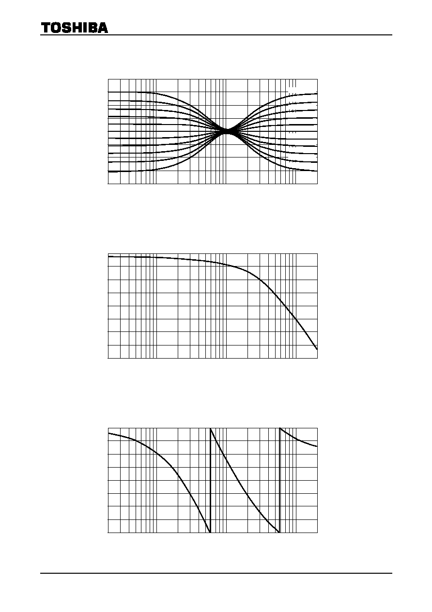
S
u
ro
un
d g
a
i
n
(dB
)
Re
la
tiv
e
g
a
in
(
d
B
)
Bus data
Volume control characteristic (L, Rch)
Gain
(dB
)
Bus data
Volume control characteristic (Wch)
Gain
(dB
)
Bus data
Wch level control characteristic
Gain
(dB
)
Bus data
Balance control characteristic
Bus data
Suround gain control characteristic
-
100
0
10
16 32 48 64
80 96 112 128
-
90
-
80
-
70
-
60
-
50
-
40
-
30
-
20
-
10
0
0
30
16
32
48
64
80 96 112 128
-
90
-
80
-
70
-
60
-
50
-
40
-
30
-
20
-
10
0
10
20
-
100
0
10
16
32
48
64
80 96 112 128
-
90
-
80
-
70
-
60
-
50
-
40
-
30
-
20
-
10
0
Lch
Rch
0
10
7
1 2 3 4 5 6
-
90
-
80
-
70
-
60
-
50
-
40
-
30
-
20
-
10
0
0
30
16 32 48 64
80 96 112 128
-
90
-
80
-
70
-
60
-
50
-
40
-
30
-
20
-
10
0
10
20
TA1343N
2002-02-12
21
Tone control characteristics
Frequency (Hz)
Re
la
tiv
e
g
a
in
(
d
B
)
Surround frequency characteristic (gain)
Frequency (Hz)
Gain
(dB
)
Surround frequency characteristic (phase)/Mode 4
f
Frequency (Hz)
P
hase
(
deg
)
7.5
-
12.5
20
-
10.0
-
7.5
-
5.0
-
2.5
0
2.5
5.0
100
1 k
10 k
20 k
180
-
180
20
-
135
-
90
-
45
0
45
90
135
100
1 k
10 k
20 k
16
-
16
20
-
12
-
8
-
4
0
4
8
12
100
1 k
10 k
20 k
Data
=
72 (h)
Data
=
68 (h)
Data
=
5E (h)
Data
=
54 (h)
Data
=
4A (h)
Data
=
40 (h)
Data
=
36 (h)
Data
=
2C (h)
Data
=
22 (h)
Data
=
18 (h)
Data
=
0E (h)

TA1343N
2002-02-12
22
Test Circuit 1
DC Characteristics
1
TP 1
10
m
F
2
TP 2
0.039
m
F
3
TP 3
0.01
m
F
4
TP 4
0.039
m
F
5
TP 5
0.039
m
F
6
TP 6
10
m
F
7
8
TP 8
10
m
F
9
TP 9
4.7
m
F
10
TP 10
0.027
m
F
11
TP 11
8200 pF
12
TP 12
24
23
22
21
20
19
18
17
16
15
14
13
TP 22
3.3
m
F
TP 21
0.01
m
F
V
CC
9 V
100
m
F
TP 19
0.022
m
F
TP 18
0.047
m
F
TP 17
0.033
m
F
TP 15
0.027
m
F
TP 14
8200 pF
TP 16
TP 13
TA
1343N
0.01
m
F
A

TA1343N
2002-02-12
23
Test Circuit 2
AC Characteristics
1
10
m
F
2
0.039
m
F
3
0.01
m
F
4
0.039
m
F
5
0.039
m
F
6
10
m
F
7
8
10
m
F
9
4.7
m
F
10
0.027
m
F
11
8200 pF
12
24
23
22
21
20
19
18
17
16
15
14
13
SDA
3.3
m
F
SW
1
0.01
m
F
(b)
0.022
m
F
0.047
m
F
0.033
m
F
0.027
m
F
8200 pF
TP 16
TP 13
TA
1343N
0.01
m
F
SCL
I
2
C Bus
TP 6
TP 8
TP 12
(a)
100
m
F
100
m
F
9 V
51
W

TA1343N
2002-02-12
24
Application Circuit
1
10
m
F
2
0.039
m
F
3
0.01
m
F
4
0.039
m
F
5
0.039
m
F
6
10
m
F
7
8
10
m
F
9
4.7
m
F
10
0.027
m
F
11
8200 pF
12
24
23
22
21
20
19
18
17
16
15
14
13
SDA
3.3
m
F
0.01
m
F
0.022
m
F
0.047
m
F
0.033
m
F
0.027
m
F
8200 pF
TA
1343N
SCL
I
2
C Bus
Lch Input
9 V
Rch Input
Wch Output
Rch Output
Lch Output
GND
10
m
F
10
m
F
10
m
F
100
m
F
0.01
m
F
TA1343N
2002-02-12
25
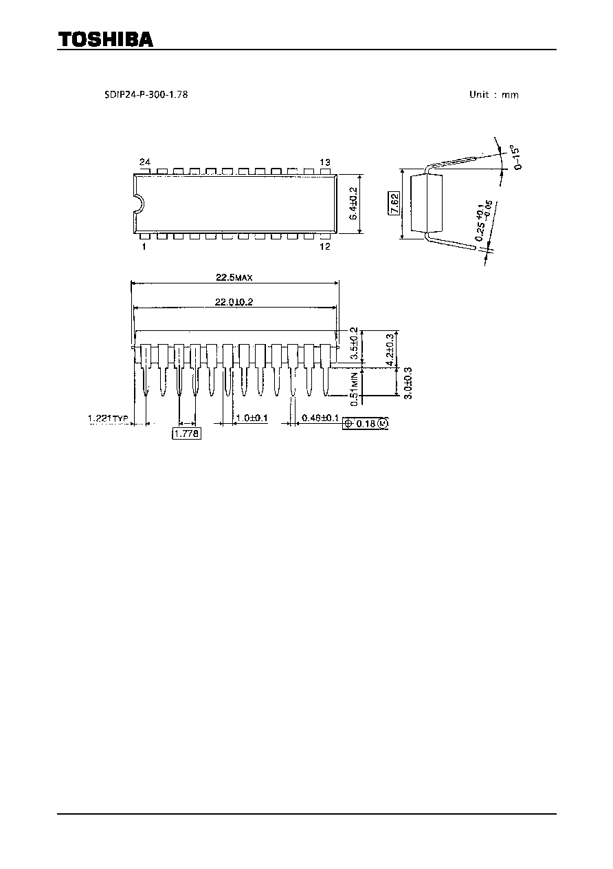
Package Dimensions
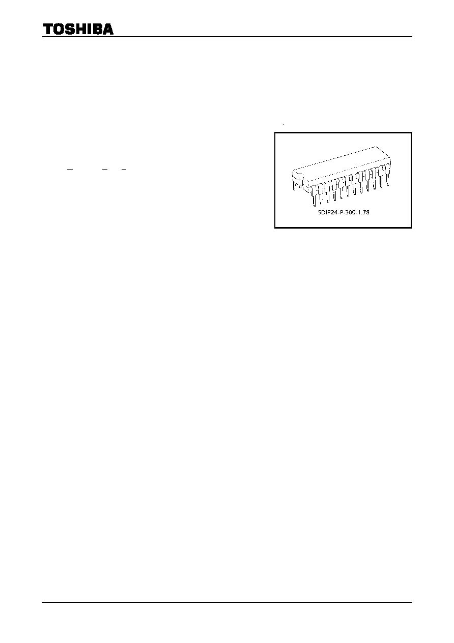
Weight: 1.22 g (typ.)

TA1343N
2002-02-12
26
∑
TOSHIBA is continually working to improve the quality and reliability of its products. Nevertheless, semiconductor
devices in general can malfunction or fail due to their inherent electrical sensitivity and vulnerability to physical
stress. It is the responsibility of the buyer, when utilizing TOSHIBA products, to comply with the standards of
safety in making a safe design for the entire system, and to avoid situations in which a malfunction or failure of
such TOSHIBA products could cause loss of human life, bodily injury or damage to property.
In developing your designs, please ensure that TOSHIBA products are used within specified operating ranges as
set forth in the most recent TOSHIBA products specifications. Also, please keep in mind the precautions and
conditions set forth in the "Handling Guide for Semiconductor Devices," or "TOSHIBA Semiconductor Reliability
Handbook" etc..
∑
The TOSHIBA products listed in this document are intended for usage in general electronics applications
(computer, personal equipment, office equipment, measuring equipment, industrial robotics, domestic appliances,
etc.). These TOSHIBA products are neither intended nor warranted for usage in equipment that requires
extraordinarily high quality and/or reliability or a malfunction or failure of which may cause loss of human life or
bodily injury ("Unintended Usage"). Unintended Usage include atomic energy control instruments, airplane or
spaceship instruments, transportation instruments, traffic signal instruments, combustion control instruments,
medical instruments, all types of safety devices, etc.. Unintended Usage of TOSHIBA products listed in this
document shall be made at the customer's own risk.
∑
The products described in this document are subject to the foreign exchange and foreign trade laws.
∑
The information contained herein is presented only as a guide for the applications of our products. No
responsibility is assumed by TOSHIBA CORPORATION for any infringements of intellectual property or other
rights of the third parties which may result from its use. No license is granted by implication or otherwise under
any intellectual property or other rights of TOSHIBA CORPORATION or others.
∑
The information contained herein is subject to change without notice.
000707EBA
RESTRICTIONS ON PRODUCT USE