 | –≠–ª–µ–∫—Ç—Ä–æ–Ω–Ω—ã–π –∫–æ–º–ø–æ–Ω–µ–Ω—Ç: TA1370FG | –°–∫–∞—á–∞—Ç—å:  PDF PDF  ZIP ZIP |
TA1370FG
2003-02-19
1
TOSHIBA Bipolar Linear Integrated Circuit Silicon Monolithic
TA1370FG
SYNC Processor, Frequency Counter IC for TV Component Signals
TA1370FG is a sync processor for TV component signals.
TA1370FG provides sync and frequency counter processing for
external input signals.
These functions are integrated in a 30 pin SSOP-type plastic
package.
TA1370FG provides I
2
C bus interface, so various functions and
controls are adjustable via the bus.
Features
∑ Horizontal synchronization circuit (28.125 kHz, 31.5 kHz,
33.75 kHz, 45 kHz)
∑ Vertical synchronization circuit (525P, 625P, 750P, 1125I, PAL 100 Hz, NTSC 120 Hz)
∑ Horizontal and vertical frequency counter
∑ Horizontal PLL
∑ Accepts 2-level and 3-level sync
∑ Accepts both negative and positive HD and VD
∑ Clamp pulse output
∑ HD, VD output (polarity inverter)
∑ Separated sync output
∑ Mask for the copy guard signal
Weight: 0.63 g (typ.)
TA1370FG
2003-02-19
2
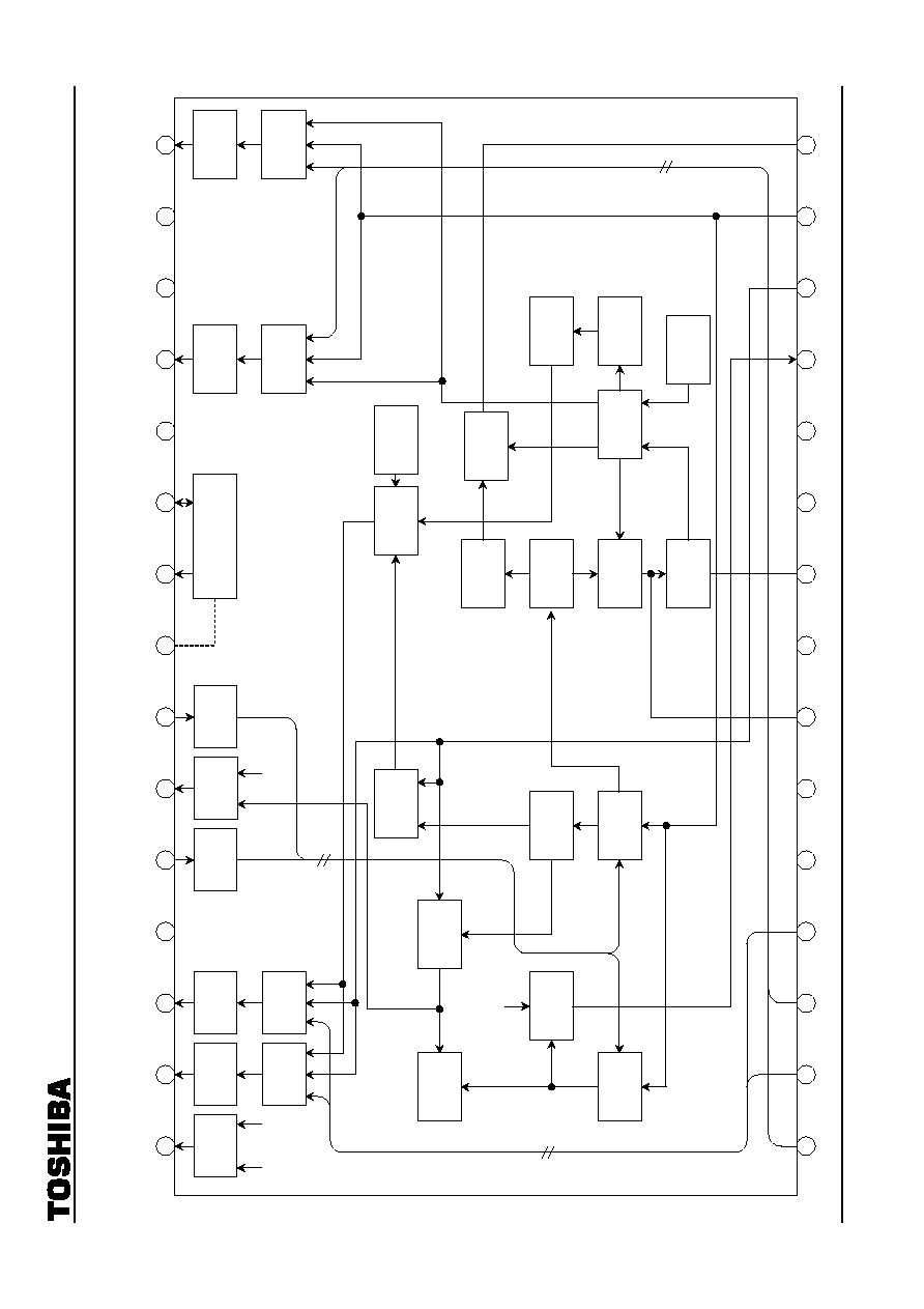
Block Diagram
30
29
28
26
25
24
23
22
21
20
19
17
DAC3
SW
INV
SW
INV
SW
SYNC
SEPA
DAC1
SW
SYNC
SEPA
INV
SW
INV
SW
I
2
CBUS
Decoder
DV2-OUT
SW
DV1-OUT
SW
HD2-OUT
SW
HD1-OUT
SW
V-Input
SW
H/V-
FREQ
Counter
V-FREQ
DET SW
DAC2
SW
H-FREQ
DET SW
V
Integral
H-INPUT
SW
V C/D
V-FREQ
SW
Clamp
Pulse
HD
Polarity
H-AFC
HVCO
CP
SW
H-FREQ
SW
2
◊ f
H
H-Ramp
H C/D
TEST DAC3
DAC1
V-SYNC
DAC2
H/C-
SYNC
DAC3 VD2-OUT
VD1-OUT
SYNC1-IN DAC1 SYNC2-IN
Address SW
SCL
SDA
HD2-OUT Digital GND
HD1-OUT
HD2-IN VD2-IN HD1-IN VD1-IN Analog
GND
AFC
Filter
HVCO V
CC
DAC2
VD3-IN
HD3-IN
CP-OUT
27
NC
18
NC
1
2
3
5
6
7
8
9
10
11
12
14
4
13
16
NC
15
NC NC NC

TA1370FG
2003-02-19
3
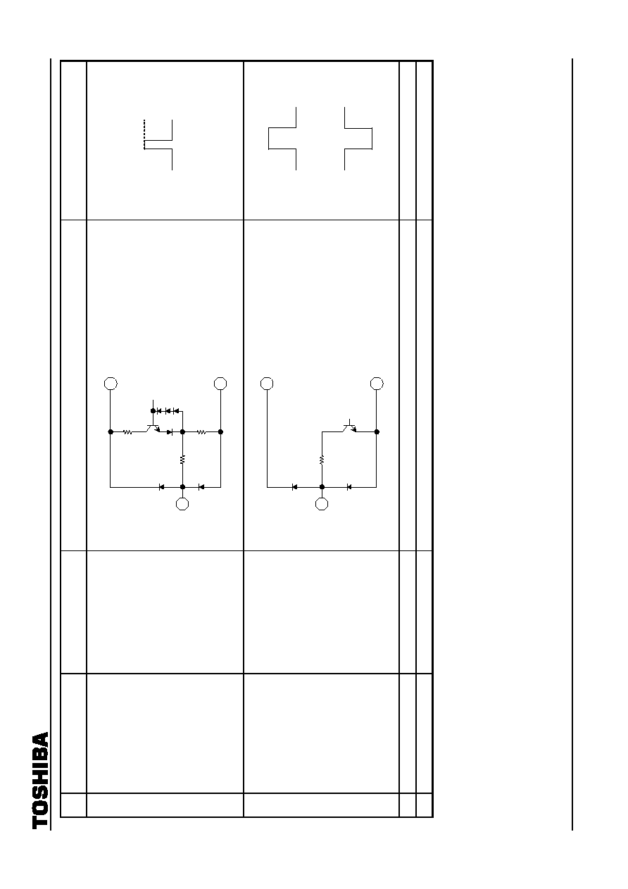
Pin Functions
Pin
No.
Pin Name
Function
Interface Circuit
Input Signal/Output Signal
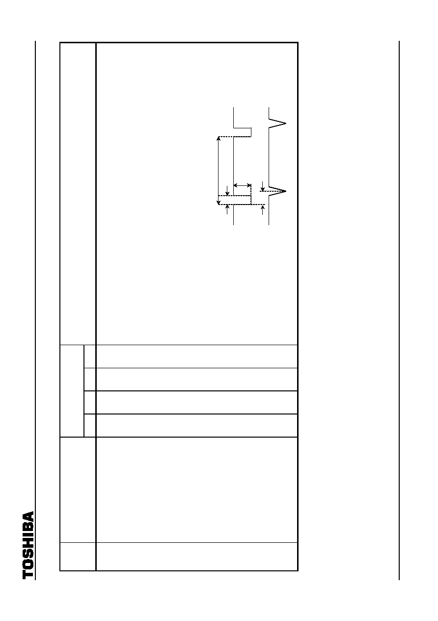
1 HD2-IN
Input horizontal sync signal.
It accepts input of both positive
and negative polarity.
Input signal from this pin is not
synchronized.
or
2 VD2-IN
Input vertical sync signal.
It accepts input of both positive
and negative polarity.
Input signal from this pin is not
synchronized.
or
11
1
5
1 k
50 k
11
2
5
1 k
45 k
Th: 0.7 V
Th: 0.7 V
Th: 0.7 V
Th: 0.7 V

TA1370FG
2003-02-19
4
Pin
No.
Pin Name
Function
Interface Circuit
Input Signal/Output Signal
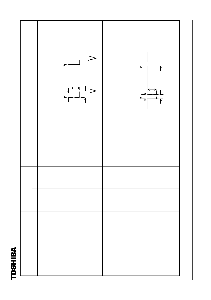
3 HD1-IN
Input horizontal sync signal.
It accepts input of both positive
and negative polarity.
Input signal from this pin is not
synchronized.
or
4 VD1-IN
Input vertical sync signal.
It accepts input of both positive
and negative polarity.
Input signal from this pin is not
synchronized.
or
5 Analog
GND
GND pin for analog circuit
blocks.
6 N.C.
Connect
to
GND.
11
3
5
1 k
50 k
11
4
5
1 k
45 k
Th: 0.7 V
Th: 0.7 V
Th: 0.7 V
Th: 0.7 V
TA1370FG
2003-02-19
5
Pin
No.
Pin Name
Function
Interface Circuit
Input Signal/Output Signal
7 AFC
Filter
Connect filter for horizontal
AFC.
Voltage on this pin determines
horizontal output frequency.
DC
8 N.C.
Connect
to
GND.
9 HVCO
Connect ceramic oscillator for
horizontal oscillation.
Use Murata
CSBLA503KECZF30.
10 N.C.
Connect
to
GND.
11 V
CC
VCC pin.
Connect 9 V (typ.).
11
7
5
300
30 k
11
9
5
4 k
1 k
2 k
1 k
10 k
TA1370FG
2003-02-19
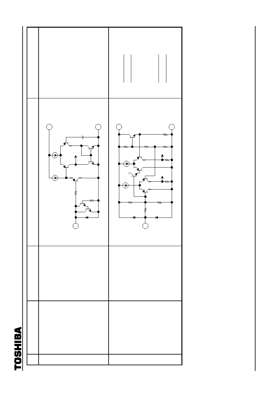
6
Pin
No.
Pin Name
Function
Interface Circuit
Input Signal/Output Signal
12 DAC2 (H/C. SYNC output)
DAC2 output pin.
In Test mode, it outputs HD or
composite sync signal to
frequency counter.
To improve the driving ability, it
is possible to connect a
resister (minimum: 2 k
)
between this pin and GND.
However, when the resister is
added, the output DC voltage
is down.
DC
or
H/C SYNC
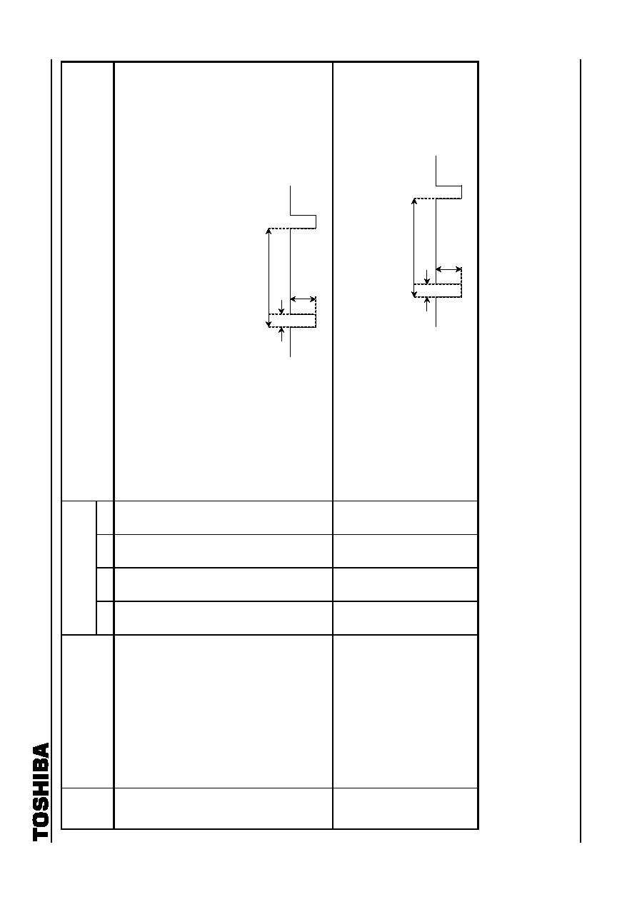
13 VD3-IN
Input vertical sync signal.
It accepts input of both positive
and negative polarity.
or
14 HD3-IN
Input horizontal sync signal.
It accepts input of both positive
and negative polarity.
or
11
14
5
1 k
50 k
11
13
5
1 k
45 k
7 V
0 V
Th: 0.7 V
Th: 0.7 V
Th: 0.7 V
Th: 0.7 V
30 k
11
12
18
200
500
TA1370FG
2003-02-19
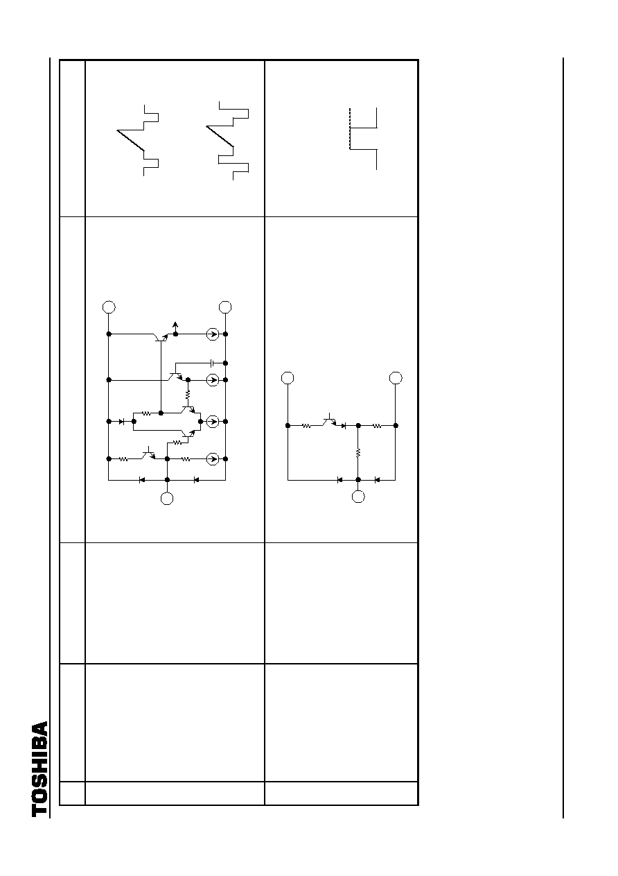
7
Pin
No.
Pin Name
Function
Interface Circuit
Input Signal/Output Signal
15 CP-OUT
Clamp pulse (CP) output pin.
It outputs CP generated by
sync circuit.
16 HD1-OUT
HD output pin.
Open collector output.
HD1/HD2 input signals are
output from this pin without
synchronization.
Polarity is switched by BUS
write function.
or
17 N.C.
Connect
to
GND.
18 Digital GND
GND pin for logic blocks.
11
16
18
200
2.
5 k
11
15
18
200
500
5.0 V
0 V
TA1370FG
2003-02-19
8
Pin
No.
Pin Name
Function
Interface Circuit
Input Signal/Output Signal
19 HD2-OUT
HD output pin.
Open collector output.
HD1/HD2 input signals are
output from this pin without
synchronization.
Polarity is switched by BUS
write function.
or
20 N.C.
Connect
to
GND.
21 SDA
SDA pin for I
2
C bus.
11
19
18
200
11
21
18
20 k
5
50
ACK
SDA
4 V
F
TA1370FG
2003-02-19
9
Pin
No.
Pin Name
Function
Interface Circuit
Input Signal/Output Signal
22 SCL
SCL pin for I
2
C bus.
23 Address
SW
Slave address switch pin.
When this pin is connected to
V
CC
(GND), used for DC/DD
H
(D8/D9
H
); when left open,
DA/DB
H
.
DA/DB
DC/DD
9 V
7.5 V
D8/D9
1.5 V
0 V
11
22
20 k
5
SCL
4 V
F
100 k
100 k
11
23
100 k
1 k
5
15 k
15 k
60 k
1.5 V
7.5 V
TA1370FG
2003-02-19
10
Pin
No.
Pin Name
Function
Interface Circuit
Input Signal/Output Signal
24 SYNC2-IN
Input Y signal (Note 1) for sync
separation circuit.
Input via clamp capacitor.
White 100
= 1 V
p
-p
or
25 DAC1
(V
SYNC
output)
DAC1 output pin.
In Test mode, it outputs VD or
composite sync signal to
frequency counter.
To improve the driving ability, it
is possible to connect a
resister (minimum: 2 k
)
between this pin and GND.
However, when the resister is
added, the output DC voltage
is down.
DC
or
V SYNC
Note 1: The signal format for SYNC1-IN (pin 26) and SYNC2-IN (pin 24)
525P/60 Hz, 625P/50Hz, 750P/60 Hz, 1125I/60 Hz, 1125I/50 Hz, NTSC Double Scan (525I/120 Hz), PAL/SECAM Double Scan (625I/100 Hz)
This IC doesn't have the sync-separation circuit for non-standard signals like weak strength signal, ghost signal and so on.
7 V
0 V
30 k
11
25
18
200
500
1 k
4 V
F
1 k
11
24
1 k
5
1 k
TA1370FG
2003-02-19
11
Pin
No.
Pin Name
Function
Interface Circuit
Input Signal/Output Signal
26 SYNC1-IN
Input Y signal (Note 1) for sync
separation circuit.
Input via clamp capacitor.
White 100
= 1 V
p
-p
or
27 N.C.
Connect
to
GND.
28 VD1-OUT
VD output pin.
Open collector output.
VD1/VD2 input signals are
output from this pin without
synchronization.
Polarity is switched by BUS
write function.
(Note) When HD PHASE will
be changed, synchronized VD
width will change. Use the start
phase of VD.
or
Note 1: The signal format for SYNC1-IN (pin 26) and SYNC2-IN (pin 24)
525P/60 Hz, 625P/50Hz, 750P/60 Hz, 1125I/60 Hz, 1125I/50 Hz, NTSC Double Scan (525I/120 Hz), PAL/SECAM Double Scan (625I/100 Hz)
This IC doesn't have the sync-separation circuit for non-standard signals like weak strength signal, ghost signal and so on.
1 k
4 V
F
1 k
11
26
1 k
5
1 k
11
28
18
200
Start phase
Start phase
TA1370FG
2003-02-19
12
Pin
No.
Pin Name
Function
Interface Circuit
Input Signal/Output Signal
29 VD2-OUT
VD output pin.
Open collector output.
VD1/VD2 input signals are
output from this pin without
synchronization.
Polarity is switched by BUS
write function.
(Note) When HD PHASE will
be changed, synchronized VD
width will change. Use the start
phase of VD.
or
30 DAC3
DAC3 output pin.
Open collector output.
In Test mode, outputs test
pulse for shipping.
DC
or
test pulse for shipping
11
29
18
200
11
30
18
500
Start phase
Start phase
TA1370FG
2003-02-19
13
Bus Control Map
Write Mode
Slave Address: D8/DA/DC
H
Preset
Sub-Add
D7
MSB
D6 D5 D4 D3 D2 D1
D0
LSB
MSB LSB
00
H-FREQUENCY
HD1/VD1-OUT SW
HD2/VD2-OUT SW
SEPA LEVEL
1000
0000
01 DAC1
DAC2
DAC3
TEST
HD1-INV
HD2-INV
1000
0000
02
V-FREQUENCY
CLP-PHS
FREQ DET SW
INPUT SW
1000
0000
03
HD
PHASE
VD1-INV VD2-INV 1000 0000
Read Mode
Slave Address: D9/DB/DD
H
D7
MSB
D6 D5 D4 D3 D2 D1
D0
LSB
0
POR
V FREQUENCY DET
1 HD-IN
H
FREQUENCY
DET
Bus Control Functions
Write Mode
(*: Preset)
∑
H-FREQUENCY (Horizontal oscillation frequency)
Switches horizontal frequency.
(00): 28.125 kHz
(01): 31.5 kHz (31.25 kHz)
*(10): 33.75 kHz
(11): 45 kHz
Horizontal frequency become 31.25 kHz when H-FREQUENCY
= (01) and V-FREQUENCY = (001)
∑
HD1/VD1-OUT SW (HD1/VD1 output switch)
Switches output from pin 16/28. When set to 00, 01, or 10, outputs HD/VD without synchronization.
When set to 11, outputs HD/VD from the sync circuit. (Note) Synchronized VD width will change, when
HD PHASE will be changed.
*(00): HD1/VD1
(01): HD2/VD2
(10): HD3/VD3
(11): Synchronized HD/VD
∑
HD2/VD2-OUT SW (HD2/VD2 output switch)
Switches output from pin 19/29. When set to 00, 01, or 10, outputs HD/VD without synchronization.
When set to 11, outputs HD/VD from the sync circuit. (Note) Synchronized VD width will change, when
HD PHASE will be changed.
*(00): HD1/VD1
(01): HD2/VD2
(10): HD3/VD3
(11): Synchronized HD/VD
∑
SEPA LEVEL (Sync separation level switch)
Switches sync separation level of pin 24/26. Set values are the levels from sync tip. Sync separation level
is changed according to the ratio of H-SYNC width during 1H period. (Note) This IC doesn't have the
sync-separation circuit for non-standard signals like weak strength signal, ghost signal and so on.
*(00): 10IRE
(01): 15IRE
(10): 20IRE
(11): 25IRE (at 1125I/60)
∑
DAC1 (DAC1 control)
Controls 2-bit DAC (pin 12).
(00): 1 V
(01): 3 V
*(10): 5 V
(11): 7 V
∑
DAC2 (DAC2 control)
Controls 2-bit DAC (pin 25).
*(00): 1 V
(01): 3 V
(10): 5 V
(11): 7 V
∑
DAC3 (DAC3 control)
Controls open collector 1-bit DAC (pin 30).
*(0): OPEN (HIGH)
(1): ON (LOW)
∑
TEST (Test mode)
Switches DAC1, 2, and 3 outputs. Also used to test IC for shipping.
*(0)
: DAC outputs are used as DAC.
(1): DAC1 outputs V. SYNC to the frequency counter.
DAC2 outputs H. SYNC or C. SYNC to the frequency counter.
DAC3 outputs IC test pulse for shipping.
TA1370FG
2003-02-19
14
∑
HD1-INV (HD1 output polarity switch)
Switches HD1 output (pin 16) polarity. When set to 0, positive HD input is output as negative HD. When
set to 0, output from the sync circuit is output as negative HD.
*(0): Normal
(1):
Inverse
∑
HD2-INV (HD2 output polarity switch)
Switches HD1 output (pin 19) polarity. When set to 0, positive HD input is output as negative HD. When
set to 0, output from the sync circuit is output as negative HD.
*(0): Normal
(1):
Inverse
∑
V-FREQUENCY (Vertical frequency switch (pull-in range))
Sets vertical frequency pull-in range, VD-STOP, or free-running frequency.
Free-running frequency is controlled by H-FREQUENCY.
Pull-in
Range
Format/H
(V)
Frequency
*(000)
48~849 H
750P/60 Hz (45 kHz)
(001)
48~725 H
625P/50 Hz (31.25 kHz)
(010) FREE-RUN
Free-running frequency is controlled by H-FREQUENCY.
(00): 562 H (01): 525 H (10): 562 H (11): 750 H
(011)
48~637 H
1125I/60 Hz (33.75 kHz), 1125I/50Hz (28.125 kHz)
(100)
48~613 H
525P/60 Hz (31.5 kHz)
(101)
48~363 H
PAL/SECAM double scan/100 Hz (31.5 kHz)
(110)
48~307 H
NTSC double scan /120 Hz (31.5 kHz)
(111)
VD STOP
VD output is HIGH
∑
CLP PHS (Clamp pulse phase switch)
Switches clamp pulse phase.
If no signal input, 0.9
µs pulse is output from the H-C/D circuit.
*(0): 1
µs (3.4%) delay following HD stop phase, 0.8 µs (2.7%) pulse
(1): 0.5
µs (1.7%) delay following HD stop phase, 0.8 µs (2.7%) pulse
∑
FREQ DET SW (Horizontal/vertical frequency counter switch)
Switches input signal used for horizontal/vertical frequency counter. This switch is controlled
independently from INPUT SW. The detection result is output as read BUS data.
*(00): SYNC1 input (01): SYNC2 input (10)/(11): HD3/VD3 inputs
∑
INPUT SW (Input signal switch for synchronization)
Switches input signal used for synchronization.
*(00): SYNC1 input
(01): SYNC2 input (10)/(11): HD3/VD3 inputs
∑
HD PHASE (HD phase adjustment)
Adjusts phase of HD output from the sync circuit. The phase of the adjustment center value is the same
as that of input H-SYNC or input HD. (Note) Synchronized VD width will change, when HD PHASE will
be changed.
(000000) :
-5% (H periodically)
*(100000) :
0%
(111111) : 5%
∑
VD1-INV (VD1 output polarity switch)
Switches VD1 output (pin 28) polarity. When set to 0, negative VD input is output as negative VD. When
set to 0, output from the sync circuit is output as negative VD.
*(0): Normal
(1):
Inverse
∑
VD2-INV (VD2 output polarity switch)
Switches VD2 output (pin 29) polarity. When set to 0, negative VD input is output as negative VD. When
set to 0, output from the sync circuit is output as negative VD.
*(0): Normal
(1):
Inverse
TA1370FG
2003-02-19
15
Read Mode
∑
POR (Power on reset)
(0): Status read (at second data read and subsequent)
(1): Power on (at first data read)
∑
HD-IN (Input signal self-check result)
Detects HD or H-SYNC input signal selected by INPUT SW.
(0): No signal input (1): Signal input
∑
V FREQ DET (Vertical frequency of SYNC or VD input selected by FREQ DET SW)
(0000000)
(0001100): No-VD
(0001101) : Vicinity of 162 Hz
(1111111) : Vicinity of 17 Hz
How to calculate vertical frequency (X):
Convert V-FREQ DET read data into decimal and define the resulting value as Y.
Where H-FREQUENCY is 31.5 kHz, Z
= 476.2 µs
Where H-FREQUENCY is 28.125 kHz/33.75 kHz/45 kHz, Z
= 474.1 µs
Vertical frequency (X)
= 1 ˜ (Y ◊ Z) [Hz]
Error of Y is
+1, -0. If vertical frequency is 162 Hz or more, the frequency cannot be accurately
measured. Time constant used to separate V.SYNC from integrated C.SYNC is 9
µs (error: ±1 µs).
∑
H FREQ DET (Horizontal frequency of SYNC or HD input selected by FREQ DET SW)
(0000000): No signal input (1111111): 53 kHz or more
How to calculate horizontal frequency (X):
X, Y, and Z are defined same as for V FREQ.
Horizontal frequency (X)
= Y ˜ (5 ◊ Z) [kHz]
Error of Y is
+1, -0. If horizontal frequency is 53 kHz or more, the frequency cannot be accurately
measured. When V-SYNC or VD is not input, horizontal frequency cannot be measured, resulting in
data
= (0000000).
Note: The start trigger for frequency counting is the internal reset-pulse made from ACK of 2nd byte in BUS
read mode. The counting period is between the first V-sync (VD) and the second V-sync (VD) after the
trigger.
The counted data will have
+1 or -0 error according to the read timing.
To assume stable data reading;
1. Set BUS reading interval more than 3 V.
2. Don't use the first data because it is unsettled.
are recommended.
Decision algorithm (detection range, detection times and so on) should be determined under
consideration of Note 1, Note 2 and the other factors such as signal strength, existence of ghost signal,
H-AFC stability, I
2
C BUS data transmission and so on via prototype TV set evaluation.
Read Timing
V-SYNC or VD
More than 3 V
Counting period 1
(to Data 1)
Counting period 2
(to Data 2)
Start trigger 1
Data 1 and
Start trigger 2
Data 2 and
Start trigger 3

TA1370FG
2003-02-19
16
Data Transfer Format via I
2
C BUS
Slave Address: D8/DA/DC
H
A6 A5 A4 A3 A2 A1 A0 W/R
1 1 0 1 1 0/1
0/1
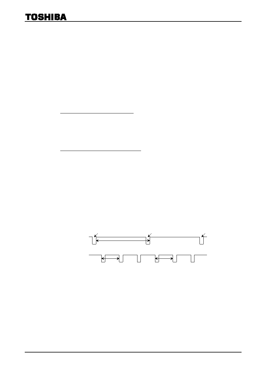
0/1
Start and Stop Condition
Bit Transfer
Acknowledge
SDA by transmitter
Only bit 9: Low impedance
Clock pulse for acknowledgment
S
Bit 9: High impedance
1 8
9
SDA by receiver
SCL from master
SDA
SCL
S
Start condition
P
Stop condition
SDA
SCL
SDA stable
Change of SDA allowed
TA1370FG
2003-02-19
17
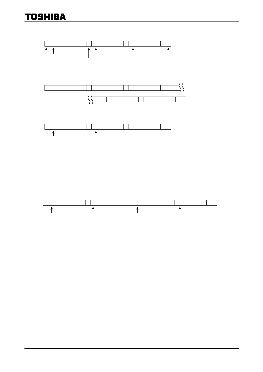
Data Transmit Format 1
Data Transmit Format 2
Data Receive Format
At the moment of the first acknowledge, the master transmitter becomes a master receiver and the slave
transmitter. This acknowledge is still generated by this slave.
The Stop condition is generated by the master.
(* important) The data read from THIS IC should always be completed in whole two words, not one word,
otherwise the IICBUS may cause error.
Optional Data Transmit Format: Automatic Increment Mode
In this transmission method, data is set on automatically incremented sub-address from the specified
sub-address.
Purchase of TOSHIBA I
2
C components conveys a license under the Philips I
2
C Patent Rights to use these
components in an I
2
C system, provided that the system conforms to the I
2
C Standard Specification as
defined by Philips.
S
Slave address
0 A
Transmit data
A
Sub address
A P
7 bit
MSB
S: Start condition
8 bit
MSB
A: Acknowledge
8 bit
MSB
P: Stop condition
S
Slave address
0 A
Transmit data
A
Sub address
A
Transmit data n
A
Sub address
A P
S
Slave address
1 A
Received data 2
A
Received data 1
A P
7 bit
MSB
8 bit
MSB
S
Slave address
A
Transmit data 2
Transmit data 1
A P
7 bit
MSB
8 bit
MSB
0
Sub address
7 bit
MSB
A 1
8 bit
MSB
TA1370FG
2003-02-19
18
Maximum Ratings
(Ta
=
=
=
= 25∞C)
Characteristics Symbol
Rating
Unit
Supply voltage
V
CCmax
12
V
Input pin signal voltage
e
inmax
9
Vp-p
Power dissipation
P
D
(Note1) 1136
mW
Power dissipation reduction rate
1/
ja
9.1 mW/
∞C
Operating temperature
T
opr
-20 to 75
∞C
Storage temperature
T
stg
-55 to 150
∞C
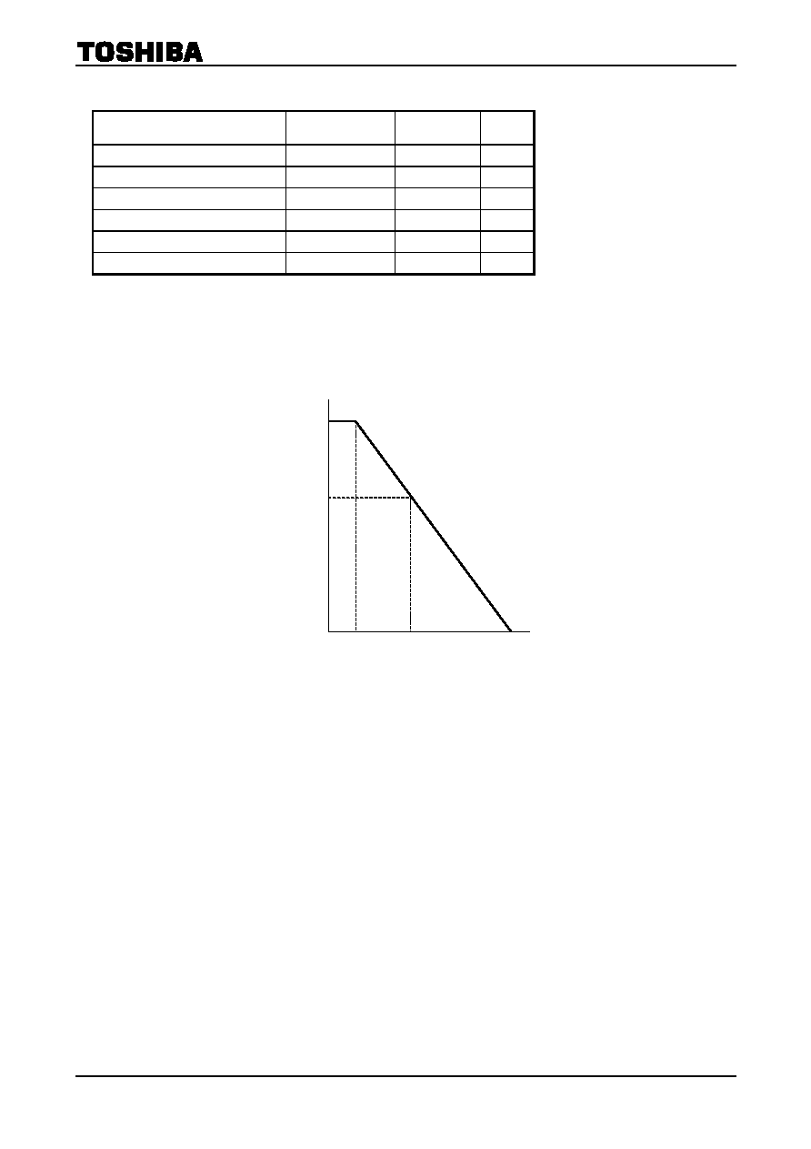
Note 1: Refer to the figure below.
Note 2: It is possible that this IC function faultily caused by leak problems according to a field intensity from CRT.
Put this IC lay-out position to CRT be far more than 20 cm. If there is not enough distance, intercept it by a
shield.
Ambient temperature Ta (∞C)
P
o
w
e
r
co
nsum
pti
on
re
duc
ti
on
ra
ti
o
P
D
(mW
)
0
150
25 75
0
682
1136
Figure P
D
- Ta Curve

TA1370FG
2003-02-19
19
Operating Condition
Characteristics Description
Min
Typ.
Max
Unit
Power supply voltage (V
CC
) Pin
11
8.5
9.0
9.5
V
HD1, HD2, HD3 Input level
Pin 3, 1, 14
2.0
5.0
9.0
VD1, VD2, VD3 Input level
Pin 4, 2, 13
2.0
5.0
9.0
Vp-p
Synchronization Pin
14
0.02
0.20 H
HD3 input width
Frequency detection Pin 14
0.45
µs
0.25H
Synchronization Pin
13
1
µs
47H
VD3 input width
Frequency detection Pin 13
1
400 µs
SYNC1, SYNC2 Input level
Pin 26, 24, white 100% with negative sync
0.9
1.0
1.1
Vp-p
HD1, HD2, VD1, VD2-OUT
Input current
Pin 16, 19, 28, 29
0.9 1.5
DAC3 Input current
Pin 30
0.5 1.0
mA
D8/D9
H
0
0
1.0
Address switching voltage
Pin 23
DC/DD
H
8.0
9.0
9.0
V
TA1370FG
2003-02-19
20
Electrical Characteristics
(V
CC
=
=
=
= 9 V, Ta ==== 25∞C, unless otherwise specified)
Current Dissipation
Pin Name
Symbol
Test
Circuit
Min Typ. Max Unit
V
CC
I
CC
32 38 44 mA
AC Characteristics
Horizontal Block
Characteristics Symbol
Test
Circuit
Test Condition
Min
Typ.
Max
Unit
S
1PH
0.6 0.7 0.8
Sync1/2 input horizontal sync phase
S
2PH
(Note HA01)
0.6 0.7 0.8
µs
HD3 input horizontal sync phase
HD
3PH
(Note
HA02)
0.6 0.7 0.8
µs
HD-
DUTY1
61 66 71
Polarity distinction active range
HD-
DUTY2
(Note HA03)
48 53 58
%
V
thS10
0.040 0.070 0.100
V
thS11
0.060 0.106 0.152
V
thS12
0.081 0.142 0.203
V
thS13
0.102 0.178 0.255
V
thS20
0.040 0.070 0.100
V
thS21
0.060 0.106 0.152
V
thS22
0.081 0.142 0.203
Sync1 input threshold amplitude
Sync2 input threshold amplitude
V
thS23
(Note HA04)
0.102 0.178 0.255
Vp-p
HD3 input threshold amplitude
(Synchronization block)
V
thHD3
(Note
HA05)
0.65 0.75 0.85 Vp-p
V
thHD1
0.65 0.
75 0.
85
V
thHD2
0.65 0.
75 0.
85
HD1 input threshold voltage
HD2 input threshold voltage
HD3 input threshold voltage
(SW block)
V
thHD3
(Note HA06)
0.65 0.
75 0.
85
Vp-p
HP0-
1.60 1.78 1.96
HP0+
1.60 1.78 1.96
HP1-
1.43 1.59 1.75
HP1+
1.43 1.59 1.75
HP2-
1.33 1.48 1.63
HP2+
1.33 1.48 1.63
HP3-
1.00 1.11 1.22
HD output phase adjustment variable
range
HP3+
(Note HA07)
1.00 1.11 1.22
µs
CP
S0
0.85 1.00 1.15
CP
W0
0.65 0.80 0.95
µs
CP
V0
4.7 5.0 5.3 V
CP
S1
0.35 0.50 0.65
CP
W1
0.65 0.80 0.95
µs
CP
V1
4.7 5.0 5.3 V
CP
S3
0
1
CP
W3
0.50 0.90 1.30
µs
Clamp pulse phase/width/level
CP
V3
(Note HA08)
4.7 5.0 5.3 V

TA1370FG
2003-02-19
21
Characteristics Symbol
Test
Circuit
Test Condition
Min
Typ.
Max
Unit
Delayed HD pulse width
W
d-HD
(Note
HA09)
1.0 1.2 1.4
µs
V16TH0
4.5 5.0 5.5
V16TL0
0.1 0.5
V16TH1
4.5 5.0 5.5
V16TL1
0.1 0.5
V16TH2
4.5 5.0 5.5
V16TL2
0.1 0.5
V16TH3
4.5 5.0 5.5
HD1 output voltage
V16TL3
0.1 0.5
V
V19TH0
4.5 5.0 5.5
V19TL0
0.1 0.5
V19TH1
4.5 5.0 5.5
V19TL1
0.1 0.5
V19TH2
4.5 5.0 5.5
V19TL2
0.1 0.5
V19TH3
4.5 5.0 5.5
HD2 output voltage
V19TL3
0.1 0.5
V
V16IH0
4.5 5.0 5.5
V16IL0
0.1 0.5
V16IH1
4.5 5.0 5.5
V16IL1
0.1 0.5
V16IH2
4.5 5.0 5.5
V16IL2
0.1 0.5
V16IH3
4.5 5.0 5.5
HD1 output voltage (polarity inverse)
V16IL3
0.1 0.5
V
V19IH0
4.5 5.0 5.5
V19IL0
0.1 0.5
V19IH1
4.5 5.0 5.5
V19IL1
0.1 0.5
V19IH2
4.5 5.0 5.5
V19IL2
0.1 0.5
V19IH3
4.5 5.0 5.5
HD2 output voltage (polarity inverse)
V19IL3
0.1 0.5
V
ID1
310 385 460
ID2
310 385 460
ID3
520 650 780
AFC phase detection current
ID4
(Note HB01)
520 650 780
µA
VCO oscillation start voltage
V
VCO
(Note
HB02)
3.9 4.2 4.5 V
TH00
1.4 1.8 2.2
TH01
1.4 1.8 2.2
TH10
1.4 1.8 2.2
HD output pulse width
(free-run)
TH11
(Note HB03)
1.4 1.8 2.2
µs

TA1370FG
2003-02-19
22
Characteristics Symbol
Test
Circuit
Test Condition
Min
Typ.
Max
Unit
F00
27.84 28.125 28.41
F01
31.19 31.5 31.82
F10
33.41 33.75 34.09
F11
44.55 45 45.45
Horizontal free-run frequency
F50
(Note HB04)
30.94 31.25 31.56
kHz
BH00
43 54 65
BH01
48 60 72
BH10
48 60 72
Horizontal oscillation control
sensitivity
BH10
(Note HB05)
71 89 107
kHz/V
VDAC
10
0.5 1.0 1.5
VDAC
11
2.7 3.0 3.3
VDAC
12
4.7 5.0 5.3
DAC1 output voltage
VDAC
13
6.5 7.0 7.5
V
VDAC
20
0.5 1.0 1.5
VDAC
21
2.7 3.0 3.3
VDAC
22
4.7 5.0 5.3
DAC2 output voltage
VDAC
23
6.5 7.0 7.5
V
VDAC
30
0.5 0.7
DAC3 output voltage
VDAC
31
8.5 8.8
V

TA1370FG
2003-02-19
23
Vertical Block
Characteristics Symbol
Test
Circuit
Test Condition
Min
Typ.
Max
Unit
V
thVD1
0.65 0.75 0.85
V
thVD2
0.65 0.75 0.85
VD1 input threshold voltage
VD2 input threshold voltage
VD3 input threshold voltage
(SW block)
V
thVD3
(Note VA01)
0.65 0.75 0.85
Vp-p
VD3 input threshold voltage
(synchronization block)
V
thVD3
(Note
VA02)
0.65 0.75 0.85 Vp-p
V28TH0
4.5 5.0 5.5
V28TL0
0.1 0.5
V28TH1
4.5 5.0 5.5
V28TL1
0.1 0.5
V28TH2
4.5 5.0 5.5
V28TL2
0.1 0.5
V28TH3
4.5 5.0 5.5
VD1 output voltage
V28TL3
0.1 0.5
V
V29TH0
4.5 5.0 5.5
V29TL0
0.1 0.5
V29TH1
4.5 5.0 5.5
V29TL1
0.1 0.5
V29TH2
4.5 5.0 5.5
V29TL2
0.1 0.5
V29TH3
4.5 5.0 5.5
VD2 output voltage
V29TL3
0.1 0.5
V
V28IH0
4.5 5.0 5.5
V28IL0
0.1 0.5
V28IH1
4.5 5.0 5.5
V28IL1
0.1 0.5
V28IH2
4.5 5.0 5.5
V28IL2
0.1 0.5
V28IH3
4.5 5.0 5.5
VD1 output voltage (polarity inverse)
V28IL3
0.1 0.5
V
V29IH0
4.5 5.0 5.5
V29IL0
0.1 0.5
V29IH1
4.5 5.0 5.5
V29IL1
0.1 0.5
V29IH2
4.5 5.0 5.5
V29IL2
0.1 0.5
V29IH3
4.5 5.0 5.5
VD2 output voltage (polarity inverse)
V29IL3
0.1 0.5
V
VP
W0
140 160 180
VP
W1
126 143 160
VP
W2
117 133 150
Vertical output pulse width
VP
W3
(Note VA03)
88 100 112
µs
TA1370FG
2003-02-19
24
Characteristics Symbol
Test
Circuit
Test Condition
Min
Typ.
Max
Unit
FV0
39.21 39.75 40.30
FV1
45.89 46.55 47.25
FV3
52.20 52.98 53.77
FV4
54.25 55.06 55.89
FV5
91.28 92.98 94.69
FV6
107.8 109.9 112.1
FV20
47.0 50.0 53.0
FV21
57.0 60.0 63.0
FV22
57.0 60.0 63.0
Vertical free-run frequency
FV23
(Note VA04)
57.0 60.0 63.0
Hz
FVPL0
311 321 332
FVPL1
624 643 663
FVPL2
668 689 710
Vertical pull-in range
FVPL3
(Note VA05)
891 918 947
Hz
28.125 kHz
6.2 7.4 8.6
31.50 kHz
5.7 6.8 7.9
33.75 kHz
5.3 6.4 7.5
Sync input-VD output phase
difference
45.00 kHz
4.4 5.2 6.0
µs
TA1370FG
2003-02-19
25
Test Conditions and Measuring Method
SW Mode
Note Item
S07 S23 S24 S26
Test Conditions and Measuring Method (V
CC
= 9 V, Ta = 25 ± 3∞C, unless otherwise specified)
HA01
Sync1/2 input horizontal sync phase
c
b
a
b
b
a
(1) Set sub-address (00) 80.
(2) SW24-a and SW26-b.
(3) Input Signal a (horizontal 33.75 kHz) to pin 26 (SYNC1-IN).
(4) Set sub-address (02) 00.
(5) Measure the phase difference S
1PH
between pin 26 and pin 7 (AFC filter) wave form.
(6) SW24-b and SW26-a.
(7) Input Signal a (33.75 kHz ) to pin 24 (SYNC2-IN).
(8) Set sub-address (02) 01.
(9) Measure the phase difference S
2PH
between pin 24 and pin 7 (AFC filter) wave form.
Signal a
Pin 7 wave form
29.63
µs
S
1PH
S
2PH
0.285 V
0.593
µs
TA1370FG
2003-02-19
26
SW Mode
Note Item
S07 S23 S24 S26
Test Conditions and Measuring Method (V
CC
= 9 V, Ta = 25 ± 3∞C, unless otherwise specified)
HA02 HD3
input
horizo
ntal sync phase
c b
(1) Set sub-address (00) 40 and (02) 02.
(2) Input signal b (horizontal 31.5 kHz) to pin 14 (HD3-IN).
(3) Measure the phase difference HD
3PH
between pin 14 and pin 7 (AFC filter) wave form.
HA03
Polarity distinction active range
c
b
(1) Set sub-address (00) 40 and (02) 02.
(2) Input signal b ((horizontal 31.5 kHz) to pin 14 (HD3-IN).
(3) Decreasing the duty of signal b to 0% (get negative period shorter), measure the duty of Signal b
(HD-DUTY1) when the phase between pin 14 and pin 16 (HD1-OUT) change.
(4) Increasing the duty of Signal b to 100% (get negative period longer), measure the duty of Signal b
(HD-DUTY2) when the phase between pin 14 and pin 16 (HD1OUT) change.
* duty
= A/(A + B) ◊ 100 (%)
Signal b
31.75
µs
1.5 V
2.35
µs
A
B
Signal b
Pin 7 wave form
31.75
µs
HD
3PH
1.5 V
2.35
µs
TA1370FG
2003-02-19
27
SW Mode
Note Item
S07 S23 S24 S26
Test Conditions and Measuring Method (V
CC
= 9 V, Ta = 25 ± 3∞C, unless otherwise specified)
HA04
Sync1 input threshold amplitude
Sync2 input threshold amplitude
c b a
b
b
a
(1) Set sub-address (00) 0B and (02) 00.
(2) Input Signal a (33.75 kHz) to pin 26 (SYNC1-IN)
(3) Measure the sync. tip DC voltage of signal a on pin 26 (SYNC1-IN). (V
sync11
)
(4) Supply external voltage via 100 k
to pin 26 and increase the voltage.
(5) Measure the sync. tip DC voltage (V
sync12
) when HD-OUT desynchronizes with signal a calculate V
thS10
.
V
thS10
= V
sync12
- V
sync11
(6) Set sub-address (00) B1, B2 and B3 and calculate V
thS11
, V
thS12
and V
thS13
as well.
(7) Calculate
V
thS20
, V
thS21
, V
thS22
and V
thS23
against pin 24 (SYNC2-IN) in the same way as 4 to 6.
HA05 HD3
input
threshold
amplitude
(synchronization block)
c b
(1) Set sub-address (03) 47 and (02) 02.
(2) Input Signal b (31.5 kHz) to pin 14 (HD3-IN).
(3) Increasing the voltage of Signal b from 0 V, measure the voltage of Signal b V
thHD3
when HD1-OUT lock.
Signal a
29.63
µs
0.285 V
0.593
µs
Signal b
31.75
µs
V
thHD1
2.35
µs
TA1370FG
2003-02-19
28
SW Mode
Note Item
S07 S23 S24 S26
Test Conditions and Measuring Method (V
CC
= 9 V, Ta = 25 ± 3∞C, unless otherwise specified)
HA06 HD1
input
threshold
voltage
HD2 input threshold voltage
HD3 input threshold voltage
(SW block)
c b
(1) Set sub-address (00) 40 and (02) 00.
(2) Input Signal b (31.5 kHz) to pin 3 (HD1-IN).
(3) Increasing the voltage of Signal b from 0 V, measure the voltage of Signal b V
thHD1
when HD1-OUT lock.
(4) Measure the voltage of pin 1 V
thHD2
. Measure the voltage of pin 14 V
thHD3
as well.
Signal b
31.5
µs
V
thHD1
2.35
µs
TA1370FG
2003-02-19
29
SW Mode
Note Item
S07 S23 S24 S26
Test Conditions and Measuring Method (V
CC
= 9 V, Ta = 25 ± 3∞C, unless otherwise specified)
HA07 HD output phase adjustment variable
range
c b
(1) Set sub-address (00) 70.
(2) Input Signal b (horizontal period T
= 35.56 µs) to pin 14 (HD3-IN).
(3) Set sub-address (02) 02.
(4) Change form 00 to 7C sub-address (03), then measure the phase change quantity (
HP0-) of pin 16
(HD1-OUT) wave form.
(5) Change form 80 to FC sub-address (03), then measure the phase change quantity (
HP0+) of pin 16
(HD1-OUT) wave form.
(6) When horizontal period of Signal b is T
= 31.75 µs measure HP1- and HP1+ as well.
(7) When horizontal period of Signal b is T
= 29.63 µs measure HP2- and HP2+ as well.
(8) When horizontal period of Signal b is T
= 22.22 µs measure HP3- and HP3+ as well.
Signal b
T
µs
1.5 V
2.35
µs
HP*+
HP*-
Pin 16 wave form
data (00)
Pin 16 wave form
data (7C) (80)
Pin 16 wave form
data (FC)
TA1370FG
2003-02-19
30
SW Mode
Note Item
S07 S23 S24 S26
Test Conditions and Measuring Method (V
CC
= 9 V, Ta = 25 ± 3∞C, unless otherwise specified)
HA08 Clamp
pulse
phase/width/level
c
b
(1) Set sub-address (00) 70.
(2) Input Signal a (horizontal 33.75 kHz) to pin 14 (HD3-IN).
(3) Set sub-address (02) 02.
(4) Measure the clamp pulse phase (CP
S0
), width (CP
W0
), output level (CP
V0
) of pin 15 (CLP-OUT) against
Signal a.
(5) Set sub-address (02) 12.
(6) Measure the clamp pulse phase (CP
S1
), width (CP
W1
), output level (CP
V1
) of pin 15 (SCP-OUT) against
Signal a.
(7) Input no-signal to pin 14.
(8) Measure the clamp pulse phase (CP
S2
), width (CP
W2
), output level (CP
V2
) of pin 15 (SCP-OUT) against pin
16 (HD-OUT).
Signal a
29.63
µs
1.5 V
2.35
µs
CP
S3
CP
W0
CP
W1
Pin 15 wave form
Pin 16 wave form
Pin 15 wave form
CP
S0
CP
S1
CP
V3
CP
V0
CP
V1
CP
W3
TA1370FG
2003-02-19
31
SW Mode
Note Item
S07 S23 S24 S26
Test Conditions and Measuring Method (V
CC
= 9 V, Ta = 25 ± 3∞C, unless otherwise specified)
HA09
Delayed HD pulse width
c
b
(1) Set sub-address (00) 70.
(2) Input Signal b (horizontal 31.5 kHz) to pin 14 (HD3-IN).
(3) Set sub-address (02) 02.
(4) Measure the pulse width (WdHD) of pin 7 (AFC filter) wave form.
Signal b
Pin 7 wave form
31.75
µs
Wd-HD
1.5 V
2.35
µs
TA1370FG
2003-02-19
32
SW Mode
Note Item
S07 S23 S24 S26
Test Conditions and Measuring Method (V
CC
= 9 V, Ta = 25 ± 3∞C, unless otherwise specified)
HB01
AFC phase detection current
OPEN
b
a
b
(1) BUS control data preset.
(2) Horizontal oscillation frequency is 28.125 kHz (00).
(3) SW7 open. Measure the Voltage of pin 7 V7 (no external supply).
(4) Connect external supply with pin 7, and supply the voltage (V7).
(5) Input signal (below figure) to pin 26 (SYNC1-IN). When INPUT SW is SYNC1-IN , measure V1 and V2 of pin
7 wave form.
(6) Supply
V7
- 0.1 V and V7 + 0.1 V to pin 7, then measure V3 and V4.
(7) Calculate by following equations.
ID1
[
µA] = (V1 [V] ˜ 1 [k]) ◊ 1000
ID2
[
µA] = (V2 [V] ˜ 1 [k]) ◊ 1000
ID3
[
µA] = (V3 [V] ˜ 1 [k]) ◊ 1000
ID4
[
µA] = (V4 [V] ˜ 1 [k]) ◊ 1000
HB02
VCO oscillation start voltage
(1) Increasing the voltage of pin 11 V
CC
form 2.5V, measure the voltage V
VCO
when pin 9 appear oscillation
wave form.
Pin 26 wave form
Pin 7 wave form
35.56
µs
0.25 V
V1, V3
V2, V4
TA1370FG
2003-02-19
33
SW Mode
Note Item
S07 S23 S24 S26
Test Conditions and Measuring Method (V
CC
= 9 V, Ta = 25 ± 3∞C, unless otherwise specified)
HB03
HD output pulse width
(free-run)
c b
(1) BUS control data preset.
(2) When horizontal oscillation frequency is 28.125 kHz (00), measure the output pulse width TH00 of pin 16
(HD1-OUT) wave form.
(3) When horizontal oscillation frequency is 31.5 kHz (01), 33.75 kHz (10), 45 kHz (11), measure the output
pulse width TH01, TH02, TH03 as well.
HB04
Horizontal free-run frequency
OPEN
b
(1) BUS control data preset.
(2) SW7 open. When horizontal oscillation frequency is 28.125 kHz (00), measure the oscillation frequency F00
of pin 16 (HD1-OUT) wave form.
(3) When horizontal oscillation frequency is 31.5 kHz (01), 33.75 kHz (10), 45 kHz (11), measure the oscillation
frequency F01, F10, F11 as well.
(4) When horizontal oscillation frequency is 31.5 kHz (01) and vertical free-run frequency is (001), measure the
oscillation frequency F50 of pin 16 wave form.
HB05
Horizontal oscillation control sensitivity OPEN
b
(1) BUS control data preset.
(2) SW7
open.
(3) Connect external voltage with pin 7 . Horizontal oscillation frequency is 28.125 kHz (00). Supply V7 (about
6.3 V)
+ 0.05 V or V7 - 0.05 V to pin 7, then measure the frequency FA, FB of pin 16 (HD1-OUT) wave form.
Calculate frequency changing ratio (BH00). BH00
= (FB - FA)/0.1
(4) When horizontal oscillation frequency is 31.5 kHz (01), 33.75 kHz (10), 45 kHz (11), calculate BH01, BH10,
BH11 as wall.
TH
Pin 16 (HD1OUT)
wave form

TA1370FG
2003-02-19
34
SW Mode
Note Item
S07 S23 S24 S26
Test Conditions and Measuring Method (V
CC
= 9 V, Ta = 25 ± 3∞C, unless otherwise specified)
VA01
VD1 input threshold voltage
VD2 input threshold voltage
VD3 input threshold voltage
(SW block)
c b
(1) Set sub-address (00) B0.
(2) Input Signal a (vertical 60 Hz) to pin 4 (VD1-IN).
(3) Set sub-address (02) 00.
(4) Increasing the voltage of Signal a from 0 V. measure the voltage of Signal b V
thVD1
when VD1-OUT lock.
(5) Measure
V
thVD2
and V
thVD3
against pin 2 and pin 13 as wall.
VA02
VD3 input threshold voltage
(synchronization block)
c b
(1) Set sub-address (00) 50.
(2) Input Signal b (vertical 60 Hz) to pin 13 (VD3-IN).
(3) Set sub-address (02) 01.
(4) Increasing the voltage of Signal b from 0 V, measure the voltage of Signal a V
thVD3
when VD1-OUT lock.
0.12 ms
16.67 ms
Signal a
V
thVD1
0.12 ms
16.67 ms
Signal a
TA1370FG
2003-02-19
35
SW Mode
Note Item
S07 S23 S24 S26
Test Conditions and Measuring Method (V
CC
= 9 V, Ta = 25 ± 3∞C, unless otherwise specified)
VA03
Vertical output pulse width
c
b
(1) Input Signal a (horizontal 33.75 kHz) to pin 14 (HD3-IN).
(2) Set sub-address (02) 02.
(3) When sub-addrss (00) is 30, measure the pulse width VPW2 of pin 28 (VD1-OUT) wave form.
(4) When sub-addrss (00) is 70, B0, F0, measure the pulse width VPW0, VPW1, VPW3 of pin 28 (VD1-OUT)
wave form as well.
VPW*
Signal a
29.63
µs
0.593
µs
Pin 28 wave form
V period
0.285 V
TA1370FG
2003-02-19
36
SW Mode
Note Item
S07 S23 S24 S26
Test Conditions and Measuring Method (V
CC
= 9 V, Ta = 25 ± 3∞C, unless otherwise specified)
VA04 Vertical
free-run
frequency
c
b
(1) Input Signal a (horizontal 33.75 kHz) to pin 14 (HD3-IN).
(2) Set sub-address (00) B0.
(3) When sub-address (02) is 02, 22, 62, 82, A2 or C2, measure the frequency FV0, FV1, FV3, FV4, FV5 or FV6
of pin 28 (VD1-OUT) wave form.
(4) Input no-signal to pin 14 (HD3-IN).
(5) Set sub-address (02) 42.
(6) When sub-address (00) is 30, 70, B0 or F0, measure the frequency FV20, FV21, FV22 or FV23 of pin 28
(VD1-OUT) wave form.
0.285 V
VPW*
Signal a
29.63
µs
0.593
µs
Pin 28 wave form
V period

TA1370FG
2003-02-19
37
SW Mode
Note Item
S07 S23 S24 S26
Test Conditions and Measuring Method (V
CC
= 9 V, Ta = 25 ± 3∞C, unless otherwise specified)
VA05 Vertical
pull-in
range
c
b
(1) Input Signal a (horizontal period T
= 35.56 µs) to pin 14 (HD3-IN).
(2) Set sub-address (02) 02.
(3) Set sub-address (00) 30.
(4) Input Signal C (vertical period initial T
= 1ms) to pin 13 (VD3-IN). Increasing vertical period of Signal C,
measure the frequency FVPL0 when pin 28 (VD1-OUT) wave form synchronize with Signal C.
(5) Input Signal a (horizontal period T
= 31.75 µs) to pin 14 (HD3-IN).
(6) Set sub-address (00) 70.
(7) Measure FVPL1 as well.
(8) Input Signal a (horizontal period T
= 29.63 µs) to pin 14 (HD3-IN).
(9) Set sub-address (00) B0.
(10) Measure FVPL2 as well.
(11) Input Signal a (horizontal period T
= 22.22 µs) to pin 14 (HD3-IN).
(12) Set sub-address (00) F0.
(13) Measure FVPL3 as well.
1.5 V
Signal a
horizontal period T
µs
0.593
µs
Signal c
V period (initial T
= 1 ms)
1.5 V
0.25 ms
Pin 28 wave form
measuring period
TA1370FG
2003-02-19
38
Test Circuit
M
0.
01
µ
F
100
Pin 12
#12
100
Pin 13
#13
100
Pin 14
#14
100
Pin 15
#15
100
Pin 1
#1
100
Pin 2
#2
100
Pin 3
#3
100
Pin 4
#4
Pin 7
#7
#9
1 k
10 k
68 k
7.
5 k
Pin 9
SW7
a
b c
2.
2
µ
F
0.
01
µ
F
100
µ
F
10 k
#30
5.
1 k
#29
5.
1 k
#28
5.
1 k
#19
100
SCL
#22
100
SDA
#21
100
Pin 25
#25
5.
1 k
#16
#26
1
µ
F
a b
SW26
SYNC1
#24
1
µ
F
a b
SW24
SYNC2 SW23
a b c
0.01
µF
#23
100
µ
F
0.
01
µ
F
100
µ
F
0.
01
µ
F
REG.
9 V 5 V
9 V
100
µ
F
0.
01
µ
F
1 k
1 k
5.
1 k
5.
1
k
75
75
10
µF
10
µF
3.
9 k
3.
9 k
TP
S
1-in
TP
S
2-in
DA
C3
VD
2
-
O
U
T
VD
1
-
O
U
T
S
Y
NC1-I
N
DA
C1
S
Y
NC2-I
N
A
ddres
s S
W
SC
L
SD
A
HD2-OUT
DI
GI
T
A
L GND
HD1-OUT
HD2-I
N
VD
2
-
IN
HD1-I
N
VD
1
-
IN
A
nal
og GND
AFC
F
ilte
r
HV
CO
V
CC
DA
C2
VD
3
-
IN
HD3-I
N
CP
-OUT
TA1370FG
M
Mylar capacitor
NC
NC
NC
30
29
28
26
25
24
23
22
21
19
16
27
20
18
17
NC
NC
NC
1
2
3
5
6
7
8
9
10
12
15
4
11
13
14
360
CS
B
L
A
503
K
E
CZF30
TA1370FG
2003-02-19
39
Application Circuit 1
(Typical values)
M
0.
01
µ
F
DAC2 VD3-IN HD3-IN CP-OUT
HD2-IN VD2-IN HD1-IN VD1-IN
7.
5 k
2.
2
µ
F
15 k
DAC3
10 k
10 k
10 k
100
SCL
100
SDA
DAC1
10 k
1
µ
F
SYNC1-
IN
1
µ
F
SYNC2-
IN
100
µ
F
0.
01
µ
F
9 V
M
Mylar capacitor
VD2-
OUT
VD1-
OUT
HD2-
OUT
HD1-
OUT
360
0.01
µF
100
µF
DA
C3
VD
2
-
O
U
T
VD
1
-
O
U
T
SYN
C
1
-
IN
DA
C1
SYN
C
2
-
IN
A
ddres
s S
W
SC
L
SD
A
HD2-OUT
DI
GI
T
A
L GND
HD1-OUT
HD2-I
N
VD
2
-
IN
HD1-I
N
VD
1
-
IN
A
nal
og GND
AFC
F
ilte
r
HV
CO
V
CC
DA
C2
VD
3
-
IN
HD3-I
N
CP
-OUT
TA1370FG
NC
NC
NC
30
29
28
26
25
24
23
22
21
19
16
27
20
18
17
NC
NC
NC
1
2
3
5
6
7
8
9
10
12
15
4
11
13
14
CSBLA503KECZF30

TA1370FG
2003-02-19
40
Application Circuit 2
(How to measure H/V frequency)
To measure H/V frequency of signal 2 (fH2: unknown) correctly, use two separated input terminals as the
following figure. One is for frequency measuring (SYNC2-in) and the other is for the AFC (SYNC1-IN). And
measure H/V frequency of signal 2 (fH2: unknown) on condition that AFC is stable (AFC locks in signal 1 (fH1:
known).) or that AFC is free-run when SYNC1-IN is no-signal.
This IC's H/V frequency counting is done by internal pulse (A) which is made in AFC circuit. So, if AFC circuit
doesn't lock in the regular frequency, the frequency of pulse (A) will not be correct and the H/V frequency data will
not be showed correct data.
Decision algorithm of H/V frequency detection (detection range, detection times and so on) should be determined
under consideration the factors such as signal strength, existence of ghost signal, H-AFC stability, I
2
C BUS data
transmission and so on via prototype TV set evaluation.
H/V FREQ
COUNTER
AFC
Internal pulse (A)
Signal 1
Signal 2
BUS READ
Signal 1
(fH1: known)
Signal 2
(fH2: unknown)
SYNC1-IN
for H-AFC
SYNC2-IN
for
H/V freq. counter
TA1370FG
TA1370FG
2003-02-19
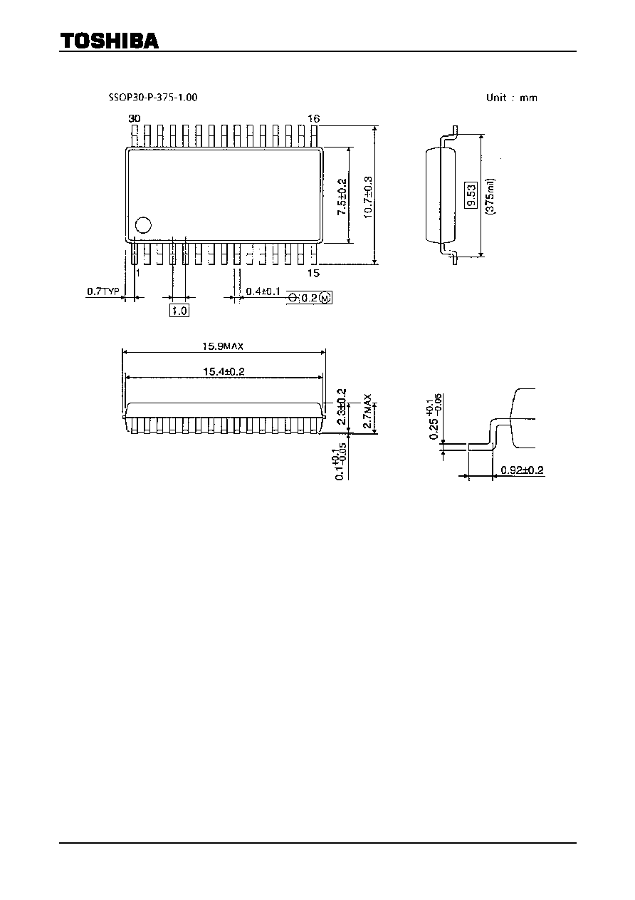
41
Package Dimensions
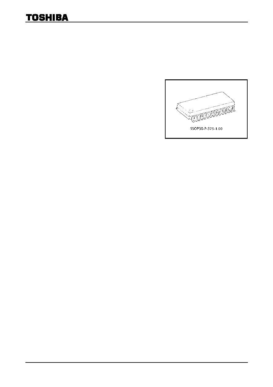
Weight: 0.63 g (typ.)

TA1370FG
2003-02-19
42
∑ TOSHIBA is continually working to improve the quality and reliability of its products. Nevertheless, semiconductor
devices in general can malfunction or fail due to their inherent electrical sensitivity and vulnerability to physical
stress. It is the responsibility of the buyer, when utilizing TOSHIBA products, to comply with the standards of
safety in making a safe design for the entire system, and to avoid situations in which a malfunction or failure of
such TOSHIBA products could cause loss of human life, bodily injury or damage to property.
In developing your designs, please ensure that TOSHIBA products are used within specified operating ranges as
set forth in the most recent TOSHIBA products specifications. Also, please keep in mind the precautions and
conditions set forth in the "Handling Guide for Semiconductor Devices," or "TOSHIBA Semiconductor Reliability
Handbook" etc..
∑ The TOSHIBA products listed in this document are intended for usage in general electronics applications
(computer, personal equipment, office equipment, measuring equipment, industrial robotics, domestic appliances,
etc.). These TOSHIBA products are neither intended nor warranted for usage in equipment that requires
extraordinarily high quality and/or reliability or a malfunction or failure of which may cause loss of human life or
bodily injury ("Unintended Usage"). Unintended Usage include atomic energy control instruments, airplane or
spaceship instruments, transportation instruments, traffic signal instruments, combustion control instruments,
medical instruments, all types of safety devices, etc.. Unintended Usage of TOSHIBA products listed in this
document shall be made at the customer's own risk.
∑ The products described in this document are subject to the foreign exchange and foreign trade laws.
∑ The information contained herein is presented only as a guide for the applications of our products. No
responsibility is assumed by TOSHIBA CORPORATION for any infringements of intellectual property or other
rights of the third parties which may result from its use. No license is granted by implication or otherwise under
any intellectual property or other rights of TOSHIBA CORPORATION or others.
∑ The information contained herein is subject to change without notice.
000707EBA
RESTRICTIONS ON PRODUCT USE