 | –≠–ª–µ–∫—Ç—Ä–æ–Ω–Ω—ã–π –∫–æ–º–ø–æ–Ω–µ–Ω—Ç: TA2028P | –°–∫–∞—á–∞—Ç—å:  PDF PDF  ZIP ZIP |

TA2028F / P
2002-10-30
1
TOSHIBA Bipolar Linear Integrated Circuit Silicon Monolithic
TA2028F,TA2028P
Filter IC For - Modulation System DA Converter
TA2028F, TA2028P are an analog filter IC for - modulation
system DA converter.
Using the TA2028F, TA2028P in combination the TC9237BF,
TC9237BN (the - modulation system DA converter with a
built-in digital filter), it is possible to construct a DA conversion
system with less external parts.
Features
∑ Built-in CR for LPFs and output (differential) amplifiers for
the left and right channel.
∑ Single power supply operation.
(+9V operation: BS tuner system)
∑ Noise distortion factor and S / N ratio are as follows
(when operating at +5V single power supply):
Noise distortion factor: -86dB (typ.)
S / N: 100dB (typ.)
Pin Connection
(top view)
Weight
SSOP16-P-225-1.00A: 0.14g (typ.)
DIP16-P-300-2.54A: 1.00g (typ.)
TA2028F / P
2002-10-30
2
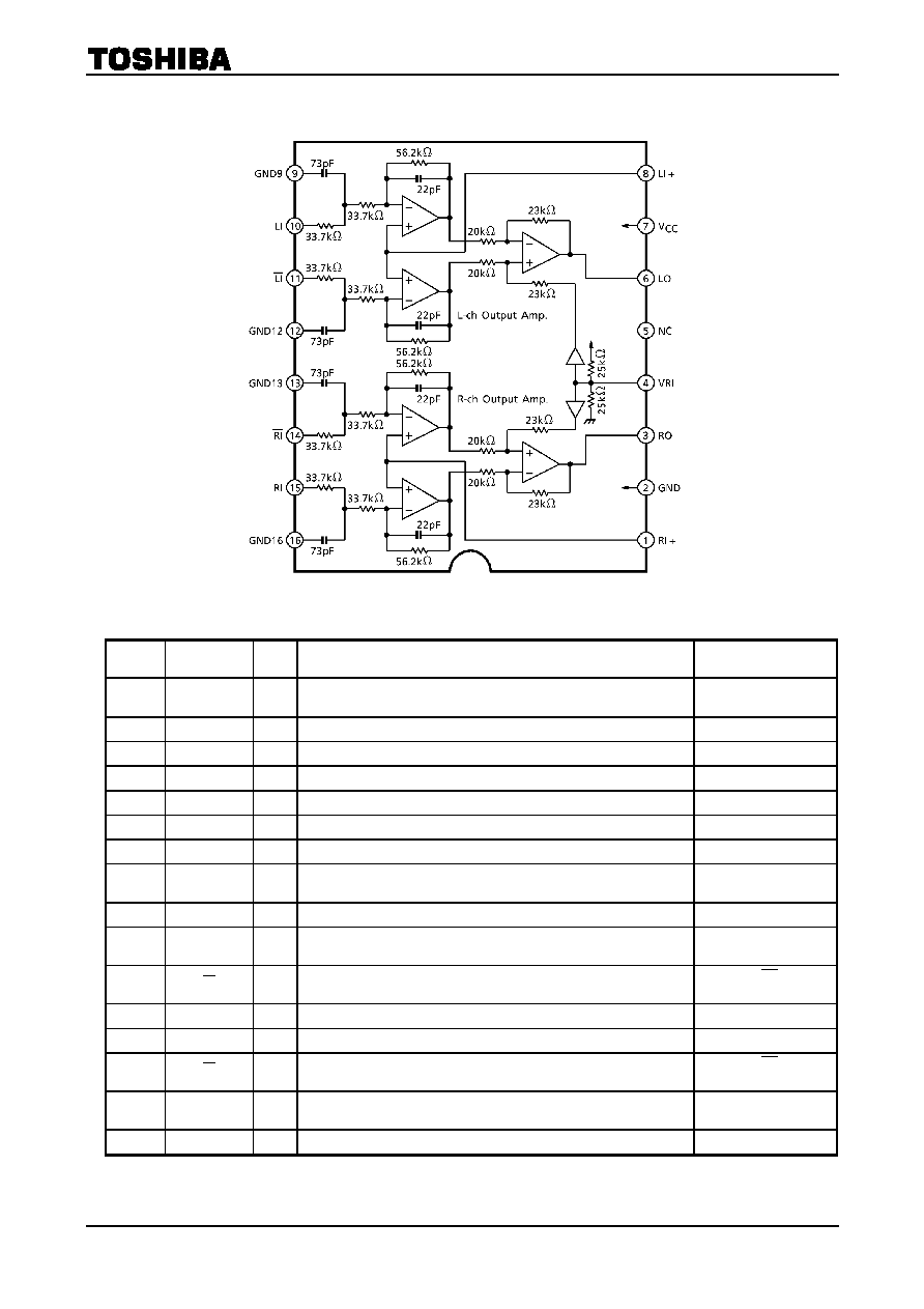
Block Diagram
Description Of Pin Functions
Pin
No.
Symbol
I / O
Function & Operation
Remarks
1 RI
+ I
R channel operational amplifier forward input pin.
Connect to VRI.
--
2 GND
--
Ground
pin.
--
3
RO
O
R channel analog output pin.
--
4
VRI
--
Reference voltage pin. (V
CC
/ 2)
See the block diagram
5 NC
--
Non
-connecting pin. NC pin is used in the open state.
--
6
LO
O
L channel analog output pin.
--
7 V
CC
--
Supply
voltage
pin.
--
8 LI
+ I
L channel operational amplifier forward input pin.
Connect to VRI.
--
9
GND9
--
Ground pin for L channel reverse input side filter.
--
10
LI
I
L channel forward input pin.
Connect to LO of
TC9237BF, TC9237BN
11
LI
I
L channel reverse input pin.
Connect to LO of
TC9237BF, TC9237BN
12
GND12
--
Ground pin for L channel forward input side filter.
--
13
GND13
--
Ground pin for R channel forward input side filter.
--
14
RI
I
R channel reverse input pin.
Connect to RO of
TC9237BF, TC9237BN
15
RI
I
R channel forward input pin.
Connect to RO of
TC9237BF, TC9237BN
16
GND16
--
Ground pin for R channel reverse input side filter.
--

TA2028F / P
2002-10-30
3
Maximum Ratings
(Ta = 25∞C)
Characteristic Symbol
Rating
Unit
Supply voltage
V
CC
11 V
TA2028F 350
(*)
Power dissipation
TA2028P
P
D
1388 (**)
mW
Operating temperature
T
opr
-25~75 ∞C
Storage temperature
T
stg
-55~150 ∞C
(*) Reduce 2.8mW / ∞C at Ta = above 25∞C.
(**) Reduce 11.2mW / ∞C at Ta = above 25∞C.
Electrical Characteristics
(unless otherwise specified, V
CC
= 5V, Ta = 25∞C)
Characteristic Symbol
Test
Cir
-
cuit
Test Condition
Min.
Typ.
Max.
Unit
Operating supply
voltage
V
CC
--
Ta
=
-35~85∞C 8.0
9.0
10
V
Operating supply
current
I
CCQ
--
At
no
signal
8.1
11.0
13.7
mA
Reference
voltage
VRI --
--
4.4 4.5 4.6 V
THD (1)
1kHz, V
o
= 2mV
rms
--
-86
-83
THD (2)
10kHz, V
o
= 2mV
rms
--
-86
-83
Noise distortion factor
THD (3)
1
1kHz, V
o
= 100mV
rms
--
-74
-70
dB
Cross talk
CT
1
1kHz, V
o
= 2mV
rms
--
-100
-90
dB
ATT (1)
40kHz, V
o
=
-10dBV
rms
0.51 0.71 1.41
Attenuation
ATT (2)
1
80kHz, V
o
=
-10dBV
rms
1.50 2.70 4.50
dB
Max. output level
V
omax
1
1kHz, THD = 1%
2.5
2.6
--
V
rms
Differential balance
G
VB
1
1kHz, 1.1dBV
rms
In
-phase input
-- --
-40
dB
LR output difference
G
VD
1
1kHz, 1.1dBV
rms
Differential input
-- 0 0.5 dB
(Note 1) When the TC9327BF, TC9237BN (+5V) and +9V single power supply are operated
: Full scale = 2mV
rms
(typ.).
(Note 2) The amount of attenuations is based on 1kHz, V
o
=
-10dBV
rms
.
(Note 3) Measuring circuit
-1: Indicates the measuring circuit.

TA2028F / P
2002-10-30
4
Test Circuit
-
-
-
-
1
SW
1
SW
2
SW
3
Measuring
Item
L
L
--
Operating supply voltage, reference voltage
L H L
Cross
talk
(RL)
H L L
Cross
talk
(LR)
H H L
Noise distortion factor, attenuation, maximum output
level, LR output difference
H H H
Difference
balance
TA2028F / P
2002-10-30
5
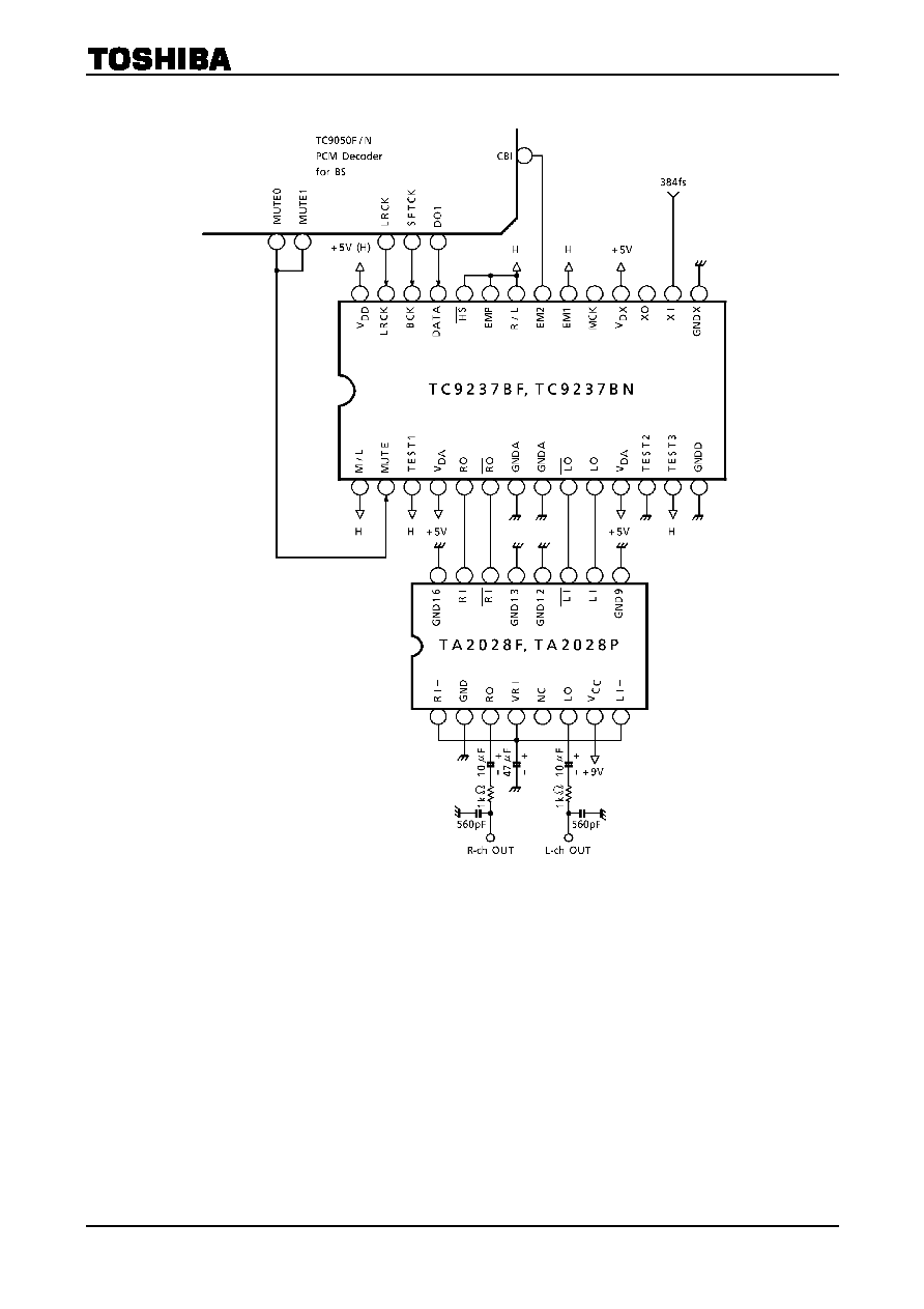
Application Circuit Example
(Cautions)
∑ Quality of crystal oscillation waveform largely effects S / N ratio.
Further, this is also true when system clock is input externally through the XI pin of pin(16).
∑ Suppress glitch of input signals (LRCK, BCK, DATA) as could as possible.
∑ The wiring between the TC9237BF, TC9237BN output and the analog filter amplifier input must be made the
shortest
∑ The capacitor between V
DA
and GNDA shall be connected as close to the pin as possible.
∑ NC pin is used in the open state.
TA2028F / P
2002-10-30
6
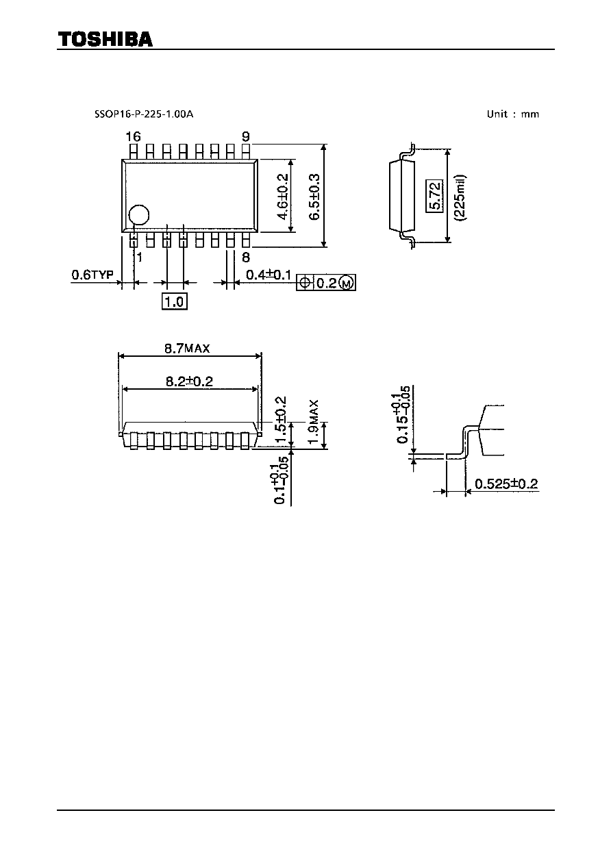
Package Dimensions
Weight: 0.14g (typ.)

TA2028F / P
2002-10-30
7
Package Dimensions
Weight: 1.00g (typ.)

TA2028F / P
2002-10-30
8
∑ TOSHIBA is continually working to improve the quality and reliability of its products. Nevertheless, semiconductor
devices in general can malfunction or fail due to their inherent electrical sensitivity and vulnerability to physical
stress. It is the responsibility of the buyer, when utilizing TOSHIBA products, to comply with the standards of
safety in making a safe design for the entire system, and to avoid situations in which a malfunction or failure of
such TOSHIBA products could cause loss of human life, bodily injury or damage to property.
In developing your designs, please ensure that TOSHIBA products are used within specified operating ranges as
set forth in the most recent TOSHIBA products specifications. Also, please keep in mind the precautions and
conditions set forth in the "Handling Guide for Semiconductor Devices," or "TOSHIBA Semiconductor Reliability
Handbook" etc..
∑ The TOSHIBA products listed in this document are intended for usage in general electronics applications
(computer, personal equipment, office equipment, measuring equipment, industrial robotics, domestic appliances,
etc.). These TOSHIBA products are neither intended nor warranted for usage in equipment that requires
extraordinarily high quality and/or reliability or a malfunction or failure of which may cause loss of human life or
bodily injury ("Unintended Usage"). Unintended Usage include atomic energy control instruments, airplane or
spaceship instruments, transportation instruments, traffic signal instruments, combustion control instruments,
medical instruments, all types of safety devices, etc.. Unintended Usage of TOSHIBA products listed in this
document shall be made at the customer's own risk.
∑ The products described in this document are subject to the foreign exchange and foreign trade laws.
∑ The information contained herein is presented only as a guide for the applications of our products. No
responsibility is assumed by TOSHIBA CORPORATION for any infringements of intellectual property or other
rights of the third parties which may result from its use. No license is granted by implication or otherwise under
any intellectual property or other rights of TOSHIBA CORPORATION or others.
∑ The information contained herein is subject to change without notice.
000707EBA
RESTRICTIONS ON PRODUCT USE