 | –≠–ª–µ–∫—Ç—Ä–æ–Ω–Ω—ã–π –∫–æ–º–ø–æ–Ω–µ–Ω—Ç: TA2069AF | –°–∫–∞—á–∞—Ç—å:  PDF PDF  ZIP ZIP |
TA2069AF
2002-10-30
1
TOSHIBA Bipolar Linear Integrated Circuit Silicon Monolithic
TA2069AF
3V Stereo Headphone Amplifier (3V USE)
The TA2069AF is developed for play-back stereo headphone
equipments (3V use).
It is built in dual preamplifiers, dual OCL power amplifiers,
motor governor, DC volume control and volume limiter etc.
Features
∑ Built-in preamplifier
Input coupling condenser-less
Built-in input capacitor for reducing buzz noise
Low noise: V
ni
= 1.2 µV
rms
(typ.)
∑ Built-in power amplifier
OCL (output condenser-less)
Voltage gain : G
V
= 31dB (typ.)
∑ Built-in motor governor
Current proportion type
∑ Built-in DC volume control function
DC volume maximum attenuation : ATT = 82dB (typ.)
∑ Built-in volume limiter function
∑ Built-in bass boost function
∑ Operating supply voltage range (Ta = 25∞C)
PRE + PW: V
CC
(opr) = 1.8~3.6V
GVN: V
CC
(opr) = 2.1~3.6V (motor voltage = 1.8V)
∑ Low supply current (V
CC
= 3V, f = 1kHz, Ta = 25∞C, typ.)
PRE + PW
Output Power
No
Signal
0.1mW ◊ 2
0.5mW ◊ 2
R
L
= 16
9.5mA 14.2mA
19.5mA
R
L
= 32
9.5mA 12.5mA
16.5mA
GVN: I
CC
= 2.5mA
Weight: 0.32g (typ.)
TA2069AF
2002-10-30
2
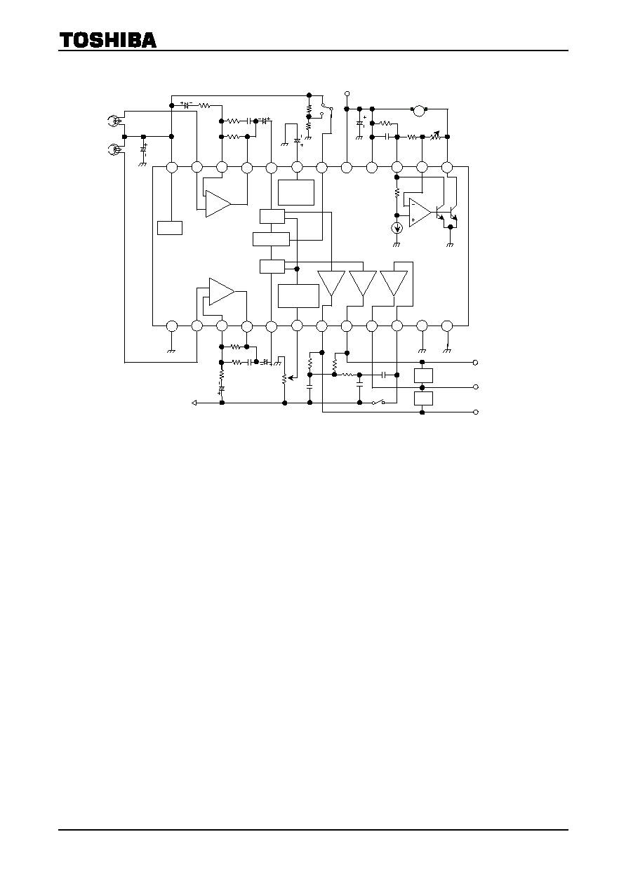
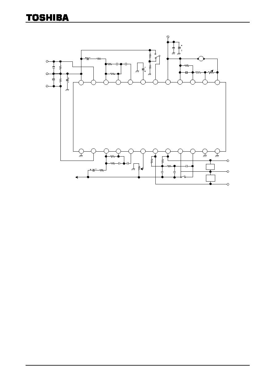
Block Diagram
OFF
PWC
PWA
PWB
PREA
VREF
PRE
INA
NFA
GND
PRE
OUTA
PW
INA
VCTL OUTB
OUTA OUTC
BST SW
OUTA
OUTC
OUTB
RL
RL
PW
INC
PW
GND
GVN
GND
VOL.
CONTROL
VOL.
LIMITER
VOL.
RIPPLE
FILTER
VREF
VREF
INB
PRE
OUTB
PW
INB
NFB
RF
IN
VLIM
ON
VCC
GVN
VCC
Rt
GVN
CTL
GVN
OUT
PREB
1
2
3
4
5
6
7
8
9
10
11
12
M
24
23
22
21
20
19
18
17
16
15
14
13
BST : OFF
TA2069AF
2002-10-30
3
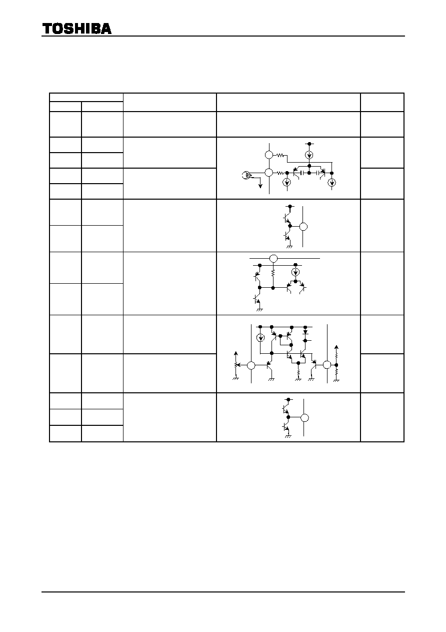
Terminal Explanation
Terminal Voltage: Typical terminal voltage at no signal with test circuit
(V
CC
= 3V, Ta = 25∞C)
Terminal
No. Name
Function Internal
Circuit
Terminal
Voltage (V)
1 PRE
GND
The GND, except for
power drive stage and
motor governer stage.
0
2 IN
A
23 IN
B
Input of preamplifier
1.2
3 NF
A
22 NF
B
NF of preamplifier
3
2
500
500
RF
VREF
1.2
4 PRE
OUT
A
21 PRE
OUT
B
Output of preamplifier
VCC
4
1.2
5 PW
IN
A
20 PW
IN
B
Input of power amplifier
RF
10K
VREF
5
1.2
6 V
CTL
The terminal of DC
volume control
This terminal can be
used also for V
LIM
terminal.
18 V
LIM
The terminal of volume
limiter level control
This terminal can be
used also for V
CTL
terminal.
VREF
VCC
VREF
6
18
7 OUT
B
8 OUT
A
9 OUT
C
Output of power
amplifier
VCC
7
1.2
TA2069AF
2002-10-30
4
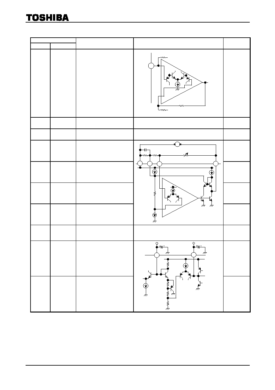
Terminal
No. Name
Function Internal
Circuit
Terminal
Voltage (V)
10 PW
IN
C
Input of center
amplifier
10
20k
VREF
30k
2k
VREF
1.2
11 PW
GND GND for power drive
stage
0
12 GVN
GND GND for motor
governor stage
0
13 GVN
OUT Motor
terminal
14 GVN
CTL
The terminal of motor
speed control
15 Rt
The terminal of amateur
compensation resistor
16 GVN
V
CC
V
CC
for motor governor
stage.
16
15
14
13
M
3
17 V
CC
V
CC
for preamplifier
stage and power
amplifier stage.
3
19 RF
IN
Ripple filter of power
supply
2.5
24 V
REF
Reference voltage
Preamplifier and
power
amplifier
operate
on
this
reference.
24
19
4k
4.7k
1.3k
10k
V
CC
1.2
TA2069AF
2002-10-30
5
Application Note
1. V
CC
and GND
This IC has two V
CC
terminals and three GND terminals. Pattern layout should be designed carefully to reduce
the common impedance.
V
CC
V
CC
(pin 17): Preamplifier stage and power amplifier stage.
GVN V
CC
(pin 16): Motor governor stage.
GND
PRE GND (pin 1): Preamplifier stage and power amplifier stage except the power drive stage.
PW GND (pin 11): Power drive stage of power amplifier.
GVN GND (pin 12): Motor governor stage.
2. V
REF
It is necessary to stabilize the V
REF
circuit, the internal circuit operate on this reference.
3. Preamplifier
Input signal should be applied to V
REF
standard, otherwise pop noise become bigger when V
CC
is turned on and
off.
4. Power amplifier
It is necessary to insert the coupling capacitor through the PW IN terminal. In case that DC current or DC
voltage is applied to the PW IN terminal, the internal circuit has unbalance and the power amplifier doesn't
operate normally.
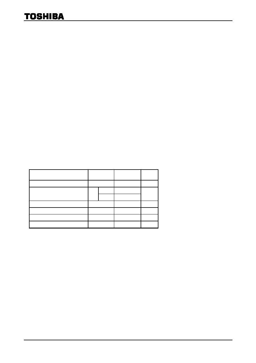
Maximum Ratings
(Ta = 25∞C)
Characteristic Symbol
Rating
Unit
Supply voltage
V
CC
4
V
(Note 1)
400
Power dissipation
P
D
(Note 2)
925
mW
Output current (PW AMP.)
I
O (PW)
200 mA
Output current (GVN)
I
O (GVN)
700
mA
Operating temperature
T
opr
-25~75 ∞C
Storage temperature
T
stg
-55~150 ∞C
(Note 1) IC only : Derated above Ta = 25∞C in the proportion 3.2mW / ∞C
(Note 2) IC + PCB (TOSHIBA typical PCB): Derated above Ta = 25∞C in the proportion 7.4mW / ∞C
TA2069AF
2002-10-30
6
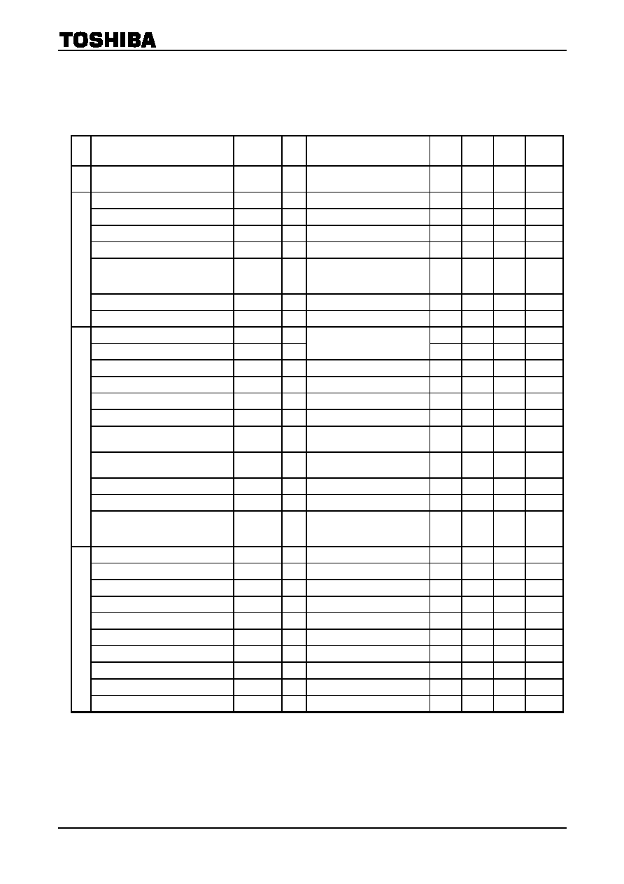
Electrical Characteristics
Unless otherwise specified, V
CC
= 3V, Ta = 25∞C, f = 1kHz, SW2: a, SW5: a
Preamplifier: R
g
= 2.2k, R
L
= 10k, SW1: ON, SW3: b, SW4: b
Power amplifier: R
g
= 600, R
L
= 16, Vol: Max, SW1: OPEN, SW3: a, SW4: a
Motor governor: I
m
= 100mA, SW1: OPEN, SW3: b, SW4: b
Characteristic Symbol
Test
Cir
-
cuit
Test Condition
Min.
Typ.
Max.
Unit
Quiescent supply current
I
CCQ
æ
PRE + PW + GVN
V
in
= 0, VOL: Min, SW4: b
æ 12 18 mA
Open loop voltage gain
G
VO
æ
V
o
=
-10dBV, SW2: b
æ 86 æ dB
Closed loop voltage gain
G
VC
æ
V
o
=
-10dBV
æ 35 æ dB
maximum output voltage
V
om
æ
THD = 1%
550
720
æ mV
rms
Total harmonic distortion
THD1
æ
V
o
=
-10dBV
æ 0.02 0.3 %
Equivalent input noise voltage
V
ni
æ
R
g
= 2.2k, SW1: OPEN
BPF = 20Hz~20kHz, NAB (G
V
= 35dB, f = 1kHz)
æ 1.2 2.4 µV
rms
Cross talk
CT1
æ
V
o
=
-10dBV
æ 70 æ dB
P
r
e
AM
P.
Ripple rejection ratio
RR1
æ
f
r
= 100Hz, V
r
=
-20dBV
æ 48 æ dB
Voltage gain 1
G
V1
æ
29 31 33 dB
Channel balance
CB
æ
V
o
=
-10dBV
-1.5 0 +1.5
dB
Voltage gain 2
G
V2
æ
V
o
=
-10dBV, SW5: b
æ 5 æ dB
Output power 1
P
o1
æ
R
L
= 16, THD = 10%
17
28
æ mW
Output power 2
P
o2
æ
R
L
= 32, THD = 10%
æ 20 æ mW
Total harmonic distortion
THD2
æ
P
o
= 1mW
æ 0.5 æ %
Output noise voltage 1
V
no1
æ
R
g
= 600, SW3: b
BPF = 20Hz~20kHz
æ 270 400 µV
rms
Output noise voltage 2
V
no2
æ
R
g
= 600, SW3: b
SW5: b, BPF = 20Hz~20kHz
æ 45 æ µV
rms
Ripple rejection ratio
RR2
æ
f
r
= 100Hz, V
r
=
-20dBV
æ 52 æ dB
Cross talk
CT2
æ
V
o
=
-10dBV
æ 32 æ dB
P
o
we
r
AM
P.
DC volume maximum attenuation
ATT
æ
V
o
=
-10dBV
SW4: ab
(VOL: Maxmin)
æ 82 æ dB
Supply current
I
CC
æ
I
m
= 0
æ 2.5 4.3 mA
Saturation voltage
V
CE (sat)
æ
I
m
= 200mA
æ
æ 0.5 V
Reference voltage
V
REF
æ
I
m
= 100mA
0.76
0.81
0.86
V
Reference voltage fluctuation 1
V
REF1
æ
V
CC
= 2.1~3.6V
æ 0.25 æ
% / V
Reference voltage fluctuation 2
V
REF2
æ
I
m
= 25~250mA
æ 0.003 æ
% / mA
Reference voltage fluctuation 3
V
REF3
æ
Ta =
-25~75∞C
æ 0.005 æ %
/
∞C
Current ratio
K
æ
34.5
37.5
40.5
Current ratio fluctuation 1
K1
æ
V
CC
= 2.1~3.6V
æ 0.25 æ
% / V
Current ratio fluctuation 2
K2
æ
I
m
= 25~250mA
æ 0.08 æ
% / mA
M
o
t
o
r Go
v
e
rnor
Current ratio fluctuation 3
K3
æ
Ta =
-25~75∞C
æ 0.005 æ %
/
∞C

TA2069AF
2002-10-30
7
Test Circuit
(a)
PW INB
(b)
SW3b
Rg = 600
(a)
(b)
600
(b)
18 k
Rg = 600
Rg = 600
PRE INA
22 µF
180
5 k
3.6 k
1 µF
8.2k
(b)
VREF
(a)
SW5
SW4
SW2a
1 µF
470 k
220 µF
22 µF
SW2b
(b) (a)
220µF (b)
PRE
INA
NFA
GND
PRE
OUTA
PW
INA
VCTL OUTB
OUTA OUTC
PW OUTA
PW OUTC
PW OUTB
RL
RL
PW
INC
PW
GND
GVN
GND
TA2069AF
VREF INB
PRE
OUTB
PW
INB
NFB
RF IN
PW
VLIM
VCC
GVN
VCC
Rt
GVN
CTL
GVN
OUT
1
2
3
4
5
6
7
8
9
10
11
12
24
23
19
17
16
15
13
(a)
470k
22µF 470
8200 pF
10 k
PRE OUTA
10 k
1 µF
1 µF
SW3a
PW INA
VREF
(a)
VREF
Rg = 600
21
PRE INB
SW1a
1000pF
2.2k
2.2k
1000pF
470
8200 pF
18 k
PRE OUTB
VREF
10k
600
1 µF
VCC
4.3k
47 µF
100 µF
5
47 µF
20
22
14
18
SW1b
TA2069AF
2002-10-30
8
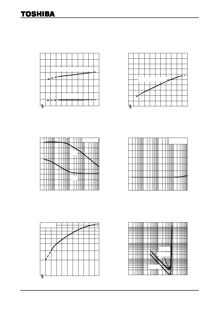
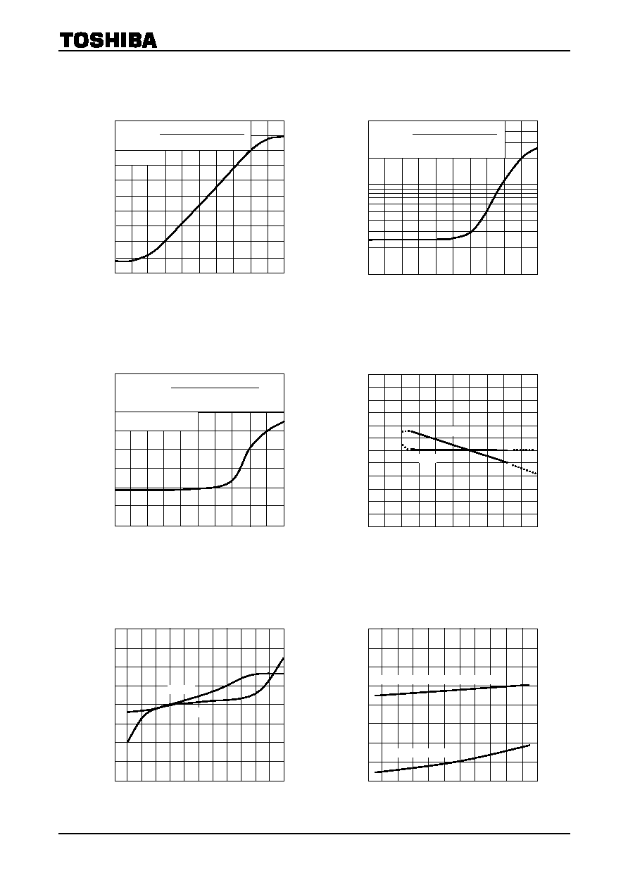
Characteristic Curves
Unless otherwise specified
V
CC
= 3V, Ta = 25∞C, f = 1kHz
Preamplifier: Rg = 2.2k, R
L
= 10k
Power amplifier: Rg = 600, R
L
= 16, Vol = max.
Motor governor: I
m
= 100mA
PRE
G
VO
, G
VC
≠ f
Frequency f (Hz)
Open l
oop
v
o
l
t
age gai
n
G
VO
(
d
B
)
Cl
os
ed l
oop
v
o
l
t
age gai
n
G
VC
(dB
)
10
100
1k 10k 100k
100
0
20
40
60
80
Vo = -10dBV
G
VO
G
VC
PRE
THD ≠ Vo
Output voltage V
o
(mV
rms
)
T
o
t
a
l
harm
oni
c
di
s
t
ort
i
on
THD
(
%
)
10
0.01
1
10 100 1000
10000
0.03
0.1
3
1
3
f = 10kHz
f = 100kHz
f = 1kHz
PRE
CT ≠ f
Frequency f (Hz)
Cros
s
tal
k
CT
(dB
)
10 100 1k 10k 100k
40
80
70
60
50
Vo = -10dBV
V
O
(DC)
≠ V
CC
Supply voltage VCC (V)
Outp
ut D
C
vol
t
a
ge
V
O
(D
C
)
(V
)
1.5
2.0 2.5 3.0 3.5 4.0
2.5
0
0.5
1.0
2.0
1.5
V
REF
PW OUT, PRE OUT
PRE
V
om
≠ V
CC
Supply voltage V
CC
(V)
M
a
x
i
m
u
m
out
put
v
o
l
t
age
V
om
(m
V
rms
)
0
1.5 2.0 2.5 3.0 3.5 4.0
1000
100
200
500
THD = 1 %
I
CCQ
, I
CC
≠ V
CC
Supply voltage VCC (V)
Qui
e
s
c
en
t su
ppl
y
cu
rr
ent
I CCQ
(m
A
)
S
uppl
y
cu
rre
nt
I
CC
(m
A
)
0
0
1.5
2.0 2.5 3.0 3.5 4.0
20
5
10
15
I
CCQ
(PRE + PW + GVN, Vol: MIN.)
I
CC
(GVN: Im = 0)
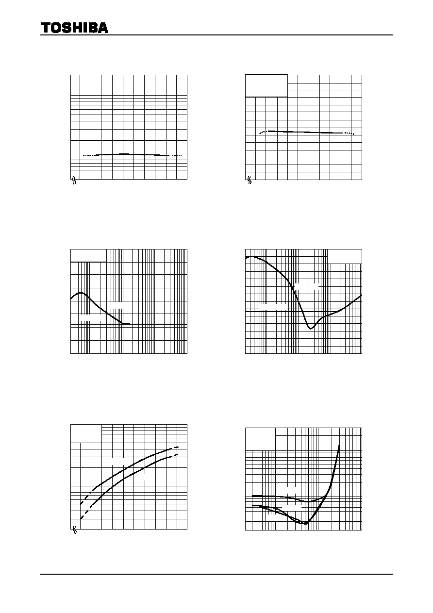
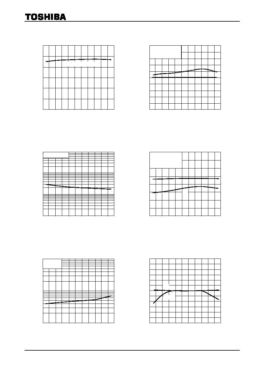
TA2069AF
2002-10-30
9
PRE
V
ni
≠ V
CC
Supply voltage V
CC
(V)
E
qui
val
ent
i
n
p
u
t
noi
s
e
v
o
l
t
a
ge
V
ni
(
µ
V
rms
)
20
0.5
0
1.5 2.0 2.5 3.0 3.5 4.0
1
2
5
10
PRE
RR ≠ V
CC
Supply voltage VCC (V)
R
i
ppl
e
rej
e
cti
on
rati
o R
R
(dB
)
10
80
0
70
60
50
40
30
20
1.5 2.0 2.5 3.0 3.5 4.0
fr = 100Hz
Vr = -20dBV
PW
G
V
≠ f
Frequency f (Hz)
V
o
l
t
age
gai
n
G
V
(dB
)
20 100
1k
10k
100k
60
20
30
40
50
BST = ON
BST = OFF
Vo = - 10dBV
PW
CT ≠ f
Frequency f (Hz)
C
r
o
ss
t
a
l
k
C
T
(
d
B)
20 100
1 10 100
0
60
50
40
30
20
10
Vo = -10dBV
BST = ON
BST = OFF
PW
P
o
≠ V
CC
Supply voltage V
CC
(V)
Out
put
power P
o
(m
W)
0 1.5
2.0
2.5
3.0
3.5
4.0
100
2
10
THD = 10%
RL = 16
32
PW
THD ≠ P
o
Output power P
o
(mW)
T
o
t
a
l
harm
oni
c
di
s
t
ort
i
on
THD
(
%
)
0.2 1
10
100
30
0.2
1
3
10
VCC = 3V
RL = 16
f = 10kHz
100Hz
1kHz
TA2069AF
2002-10-30
10
GVN
V
REF
, K ≠ V
CC
Supply voltage V
CC
(V)
Ref
e
renc
e v
o
l
t
age f
l
u
c
t
uat
i
on
V
REF
(
m
V
)
Current
rat
i
o
f
l
uct
uat
i
o
n
K
- 7.5
1.5 2.0 2.5 3.0 3.5 4.0
7.5
- 5.0
- 2.5
0.0
2.5
5.0
VREF
K
1
PW
V
no
≠ Vol.
Volume ratio
Outp
ut noi
s
e
v
o
l
t
a
ge
V
no
(
µ
V
rms
)
0 0.2 0.4 0.6 0.8
500
10
20
50
100
200
Volume Resistance
(PIN(6)
- GND)
ratio
Volume resistance
=
PW
RR ≠ Vol.
Volume ratio
Ri
ppl
e
rej
e
ct
i
on
rat
i
o
RR
(dB
)
0 0.2 0.4 0.5 0.8 1
40
80
70
60
50
fr = 100Hz, Vr = -20dBV
Resistance (PIN(6) - GND)
Volume resistance
Volume ratio =
-10
GVN
V
REF
, K ≠ I
m
Motor current I
m
(mA)
Ref
e
renc
e v
o
l
t
age f
l
u
c
t
uat
i
on
V
REF
(
m
V
)
Current
rat
i
o
f
l
uct
uat
i
o
n
K
0 50 100 150 200 250 300
10
- 5
0
5
VREF
K
GVN
I
CCQ
, I
CC
≠ Ta
Ambient temperature Ta (∞C)
Qui
e
sc
ent
s
uppl
y
c
u
rrent
I
CCQ
(m
A
)
S
uppl
y c
u
rren
t
I
CC
(m
A
)
- 20
0
20
40
60
80
20
0
5
10
15
ICCQ (PRE + PW + GVN, Vol.=MIN)
ICC (GVM : Im = 0)
PW
V
o
≠ Vol.
Volume ratio
Outp
ut
vol
t
ag
e V
o
(dB
)
0 0.2 0.4 0.6 0.8 1
10
- 90
- 70
- 50
- 30
- 10
=
Volume Resistance
(PIN(6)
- GND)
ratio
Volume resistance
0dB = -10dBV
=
TA2069AF
2002-10-30
11
PRE
THD ≠ Ta
Ambient temperature Ta (∞C)
T
o
t
a
l
harm
oni
c
di
s
t
ort
i
on
THD
(
%
)
1
0.001
-
20 0 20 40 60 80
0.01
0.1
Vo = -10dBV
V
O (DC)
≠ Ta
Ambient temperature Ta (∞C)
Outp
ut D
C
vol
t
a
ge
V
O
(DC)
(V
)
-
20 0 20 40 60 80
1.5
0
0.5
1
VREF, PW OUT, PRE OUT
PRE
G
V
, V
om
≠ Ta
Ambient temperature Ta (∞C)
V
o
l
t
ag
e g
a
i
n
G
V
(dB
)
Vom
GV
-
20
0 20 40 60 80
40
30
600
640
680
32
34
36
38
720
760
800
Maxi
mu
m
o
u
t
put
vol
t
ag
e V
om
(mV
rm
s)
GV : Vo = -10dBV
Vom : THD = 1%
GVN
V
REF
, K ≠ Ta
Ambient temperature Ta (∞C)
Ref
e
renc
e v
o
l
t
age f
l
u
c
t
uat
i
on
V
REF
(
m
V
)
Current
rat
i
o
f
l
uct
uat
i
o
n
K
- 6
- 20
0
20
40
60
80
- 4
- 2
6
0
2
4
K
VREF
PW
THD ≠ Ta
Ambient temperature Ta (∞C)
T
o
t
a
l
harm
oni
c
di
s
t
ort
i
on
THD
(
%
)
0.1
-
20 0 20 40 60 80
10
0.2
0.5
1
2
5
Po = 1mW
PW
G
V
, P
o
≠ Ta
Ambient temperature Ta (∞C)
V
o
l
t
age
gai
n
G
V
(dB
)
GV
10
-
20
0 20 40 60 80
25
35
20
40
30
50
30
Outp
ut pow
er
P
o
(mW
)
GV : Vo = -10dBV
Po : THD = 10%
Po
TA2069AF
2002-10-30
12
Application Note
18 k
VCC
8.2k
470 k
22 µF
8200 pF
22 µF
PRE
INA
NFA
GND
PRE
OUTA
PW
INA
VCTL
OUTB
OUTA
OUTC
OUTA
OUTC
OUTB
RL
PW
INC
PW
GND
GVN
GND
TA2069AF
VREF INB
PRE
OUTB
PW
INB
NFB
RF IN
PW
VLIM
VCC
GVN
VCC
Rt
GVN
CTL
GVN
OUT
1
2
3
4
5
6
7
8
9
10
11
12
24
23
19
17
16
15
13
470k
8200 pF
12 k
VREF
1 µF
0.1 µF
BST SW BST : OFF
21
PRE INB
2.2k
1000pF
18 k
4.3k
100 µF
180
20
22
14
18
22 µF
2.2k
1000pF
470 k
1 µF
1 µF
3.6 k
5 k
0.1 µF
47 µF
VREF
PRE INA
M
470
0.1 µF
33k
33k
10k
0.1 µF
RL
TA2069AF
2002-10-30
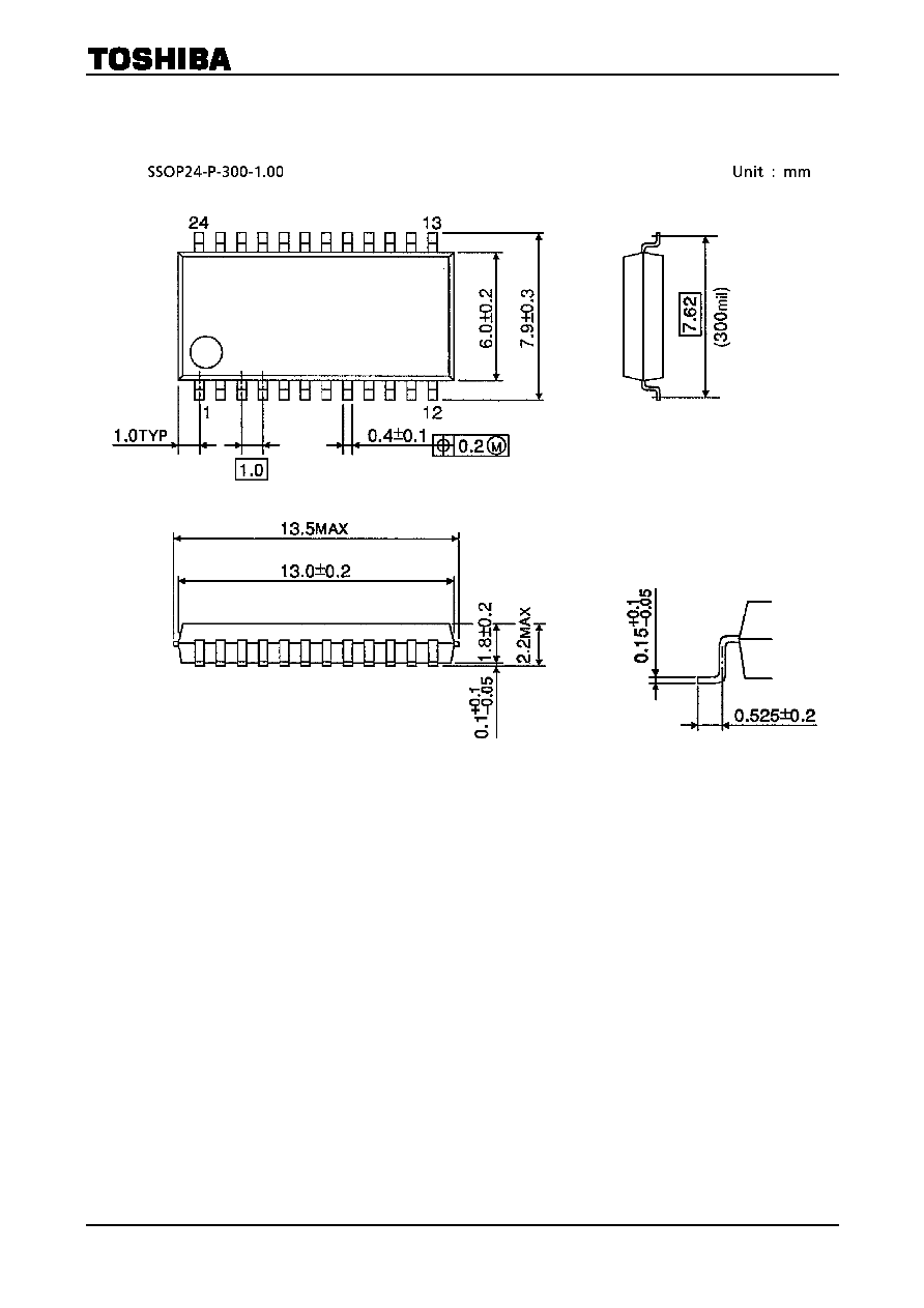
13
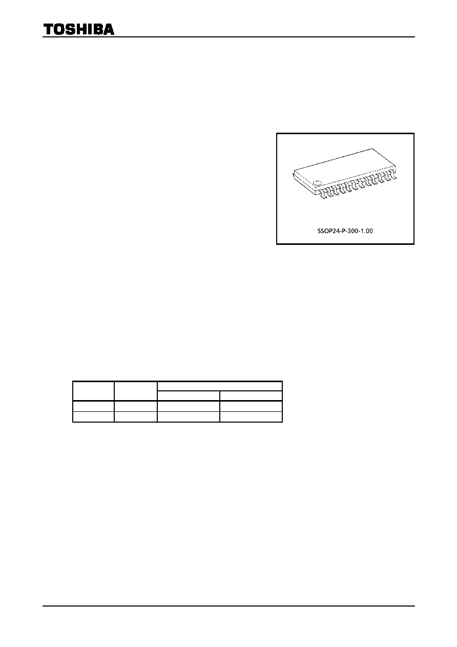
Package Dimensions
Weight: 0.32g (typ.)

TA2069AF
2002-10-30
14
∑ TOSHIBA is continually working to improve the quality and reliability of its products. Nevertheless, semiconductor
devices in general can malfunction or fail due to their inherent electrical sensitivity and vulnerability to physical
stress. It is the responsibility of the buyer, when utilizing TOSHIBA products, to comply with the standards of
safety in making a safe design for the entire system, and to avoid situations in which a malfunction or failure of
such TOSHIBA products could cause loss of human life, bodily injury or damage to property.
In developing your designs, please ensure that TOSHIBA products are used within specified operating ranges as
set forth in the most recent TOSHIBA products specifications. Also, please keep in mind the precautions and
conditions set forth in the "Handling Guide for Semiconductor Devices," or "TOSHIBA Semiconductor Reliability
Handbook" etc..
∑ The TOSHIBA products listed in this document are intended for usage in general electronics applications
(computer, personal equipment, office equipment, measuring equipment, industrial robotics, domestic appliances,
etc.). These TOSHIBA products are neither intended nor warranted for usage in equipment that requires
extraordinarily high quality and/or reliability or a malfunction or failure of which may cause loss of human life or
bodily injury ("Unintended Usage"). Unintended Usage include atomic energy control instruments, airplane or
spaceship instruments, transportation instruments, traffic signal instruments, combustion control instruments,
medical instruments, all types of safety devices, etc.. Unintended Usage of TOSHIBA products listed in this
document shall be made at the customer's own risk.
∑ The products described in this document are subject to the foreign exchange and foreign trade laws.
∑ The information contained herein is presented only as a guide for the applications of our products. No
responsibility is assumed by TOSHIBA CORPORATION for any infringements of intellectual property or other
rights of the third parties which may result from its use. No license is granted by implication or otherwise under
any intellectual property or other rights of TOSHIBA CORPORATION or others.
∑ The information contained herein is subject to change without notice.
000707EBA
RESTRICTIONS ON PRODUCT USE