 | –≠–ª–µ–∫—Ç—Ä–æ–Ω–Ω—ã–π –∫–æ–º–ø–æ–Ω–µ–Ω—Ç: TA2125AF | –°–∫–∞—á–∞—Ç—å:  PDF PDF  ZIP ZIP |

TA2125AF
2002-02-12
1
TOSHIBA Bipolar Liner Integrated Circuit Silicon Monolithic
TA2125AF
Power Driver IC for CD Player
TA2125AF is power driver IC developed for CD players.
This IC have built-in 4 channel BTL power amplifiers and 1
channel H-Bridge driver.
Which drives focus-coil and tracking coil for 3-beam pick-up head,
disc motor, feed motor and loading motor.
Featuers
∑ 4 channel BTL linear drivers
High output power: V
out
= 5.1 Vp-p (V
CC
= 8 V, R
L
= 8 )
Stand-by switch for BTL drivers
∑ 1 channel H-Bridge: V
CE (H)
+ V
CE (L)
= 1.3 V (V
R
= V
M
= 8 V,
I
O
= 200 mA)
Logic control (forward, revers, brake, stand-by)
∑ Punch through current restriction diode for H-bridge
∑ 5 V regulator reference amp (with external output Tr.)
∑ Thermal shut down protection
∑ Operating supply voltage range: V
CC
= 5.0-9.0 V
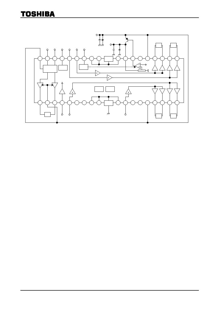
Block Diagram
Weight:
g (typ.)
Preliminary
24
6
7
12
13
1
2
RL5
36
V
R
35 34 33 32 31 30
Control
Logic
3
STBY
STBY
RIN
FIN
4ch
Driver
STB
IN3
IN4
REG
STB
29
27
28
FIN
V
CC
26
25
REG OUT
N.C.
23
22 21
¥
3
¥
3
¥
3
¥
3
20 19
4
VCIN
IN1
5
N.C.
N.C.
¥
3
¥
3
¥
3
¥
3
15 16 17 18
IN2
N.C. N.C.
11
14
8
9
FIN
10
GND
Iref
TSD
RL4
RL3
RL2
RL1
TA2125AF
2002-02-12
2
Terminal Explanation
No. Symbol
Function
1 OUT5A
Output
terminal
H-bridge
2 V
M
Supply voltage terminal for Logic
H-bridge
3 OUT5B
Output
terminal
H-bridge
4 V
CIN
Input reference voltage
4ch BTL
5
IN1
Input for ch1
4ch BTL
6 N.C.
Open
æ
7 N.C.
Open
æ
8
N.C.
8, 9, 10, 27, 28, 29 are connected to PW GND (FIN)
æ
9
N.C.
8, 9, 10, 27, 28, 29 are connected to PW GND (FIN)
æ
10
N.C.
8, 9, 10, 27, 28, 29 are connected to PW GND (FIN)
æ
11
IN2
Input for ch2
4ch BTL
12 N.C.
Open
æ
13 N.C.
Open
æ
14 V
CC1
Supply voltage terminal for ch1/ch2
4ch BTL
15
OUT2M
Inverted output for ch2
4ch BTL
16
OUT2P
Non-inverted output for ch2
4ch BTL
17
OUT1M
Inverted output for ch1
4ch BTL
18
OUT1P
Non-inverted output for ch1
4ch BTL
19
OUT3P
Non-inverted output for ch3
4ch BTL
20
OUT3M
Inverted output for ch3
4ch BTL
21
OUT4P
Non-inverted output for ch4
4ch BTL
22
OUT4M
Inverted output for ch4
4ch BTL
23 V
CC2
Supply voltage terminal for ch3/ch4
4ch BTL
24 N.C.
Open
æ
25
REG
Connection with BASE of PNP Tr
Regulator
26
REG OUT Output for regulator (5 V)
Regulator
27
N.C.
8, 9, 10, 27, 28, 29 are connected to PW GND (FIN)
æ
28
N.C.
8, 9, 10, 27, 28, 29 are connected to PW GND (FIN)
æ
29
N.C.
8, 9, 10, 27, 28, 29 are connected to PW GND (FIN)
æ
30
REG STBY Standby control for regulator
Regulator
31
IN4
Input for ch4
4ch BTL
32
IN3
Input for ch3
4ch BTL
33
STBY
Standby control for 4ch BTL
4ch BTL
34 FIN
Logic
control
input
H-bridge
35 RIN
Logic
control
input
H-bridge
36
VR
Supply voltage terminal for motor driver
H-bridge
TA2125AF
2002-02-12
3
Precaution Use
(4ch BTL)
∑ Input stage
Minimum input DC voltage range for buffer is 0.2 V
∑ Driver stage
Each channel driver consists of BTL configuration linear amplifier.
Voltage gain is fixed: Gv = 15.2dB
∑ VCIN terminal
VCIN is reference voltage terminal for input signal
∑ GND
Pin 8~10 and Pin 27~29 are connected to FIN through inner lead frame.
Each FIN are not connected each other also.
The heat of power dissipation is transferred to PCB, through PW-GND Pin. PW GND is connected to substrate of
Pellet to connected copper foil area as large as possible.
∑ V
CC1
/V
CC2
Pin 14 and pin 23 are not connected through AL layer on chip.
(H-Bridge)
∑ VR/VM terminal
VR terminal is control for H-brige dynamic range. I36 = 30 mA (Brake Mode)
VM terminal is V
CC
terminal for H-Bridge.
∑ STBY/REG STBY
STBY is standby control terminal for 4ch BTL.
REG STBY is standby control terminal for regulator.
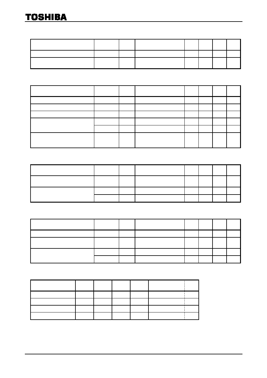
Maximum Ratings
(Ta
=
=
=
=
25∞C)
Characteristics Symbol
Rating
Unit
Supply voltage
V
CC
12 V
Power dissipation
P
D
1.7
W
Operating temperature
T
opr
-
35~85
∞C
Storage temperature
T
stg
-
55~150 ∞C
TA2125AF
2002-02-12
4
Electrical Characteristics
(Unless otherwise specified, V
CC
=
=
=
=
8 V, R
L
=
=
=
=
8
W
W
W
W
, VBIAS
=
=
=
=
2.1 V, f
=
=
=
=
1 kHz, Ta
=
=
=
=
25∞C)
Characteristics Symbol
Test
Circuit
Test Condition
Min
Typ.
Max
Unit
Operating supply voltage
V
CC
1, 2
æ
æ
5 8 9 V
Quiescent current
I
ccq
æ
V
IN
=
VBIAS, R
L
=
OPEN
(With out H-SW)
27 37 60 mA
4ch BTL Driver
Characteristics Symbol
Test
Circuit
Test Condition
Min
Typ.
Max
Unit
Output offset voltage
V
OS
æ
R
g
=
0
-
50 10 50 mV
Maximum output voltage
V
OM
æ
V
IN
=
4 V/GND
4.5
5.1
æ
V
Voltage gain
Gv
æ
V
IN
=
VBIAS
±
200
mV
14.0 15.2 16.4
dB
V
STB (on)
æ
æ
æ
0.5 V
Stand-by 1 control voltage
V
STB (off)
æ
3.0
æ
æ
V
Stand-by current
I
STB1
æ
V
IN
=
VBIAS, R
L
=
OPEN
H-Bridge: Stand-by
5 V REG: Stand-by
æ
æ
1
m
A
Regulator Reference Amp
Characteristics Symbol
Test
Circuit
Test Condition
Min
Typ.
Max
Unit
Output voltage
V
reg
æ
I
o
=
200 mA
Tr. 2SA1203Y
4.6 5 5.2 V
V
reg (on)
æ
2.5
æ
V
CC
V
Regulator control voltage
V
reg (off)
æ
GND
æ
1.5 V
H-Bridge
Characteristics Symbol
Test
Circuit
Test Condition
Min
Typ.
Max
Unit
Output saturation voltage
V
CE
æ
I
o
=
200 mA
æ
1.3 1.4 V
Stand-by current
I
STB2
æ
4ch BTL: Stand-by
5 V REG: Stand-by
æ
æ
1
m
A
V
HB (on)
æ
2.5
æ
V
CC
V
Control voltage
V
HB (off)
æ
GND
æ
0.7 V
H-Bridge Control Logic/V
R
Current
(36pin)
Operation Mode
Fin
Rin
Out5A
Out5B
V
R
Current
Unit
Forward H
L
L
H
19.5
mA
Revers L
H
H
L
19.5
mA
Brake H
H
L
L
30
mA
Stand-by L
L
Open
Open
1
m
A
TA2125AF
2002-02-12
5
Test Circuit
24
6
7
12
13
1
2
RL5
36 35 34 33 32 31 30
Control
Logic
3
STBY
STBY
29
27
28
FIN
26
25
100
m
F
N.C.
23
22 21
RL4
¥
3
¥
3
¥
3
¥
3
20 19
RL3
4
5
N.C.
N.C.
¥
3
¥
3
¥
3
¥
3
RL2
RL1
15 16 17 18
N.C. N.C.
11
14
8
9
FIN
10
GND
0.
1
m
F
0.
1
m
F
47
m
F
Iref
TSD

TA2125AF
2002-02-12
6
Package Dimensions
Weight:
g (typ.)

TA2125AF
2002-02-12
7
∑
TOSHIBA is continually working to improve the quality and reliability of its products. Nevertheless, semiconductor
devices in general can malfunction or fail due to their inherent electrical sensitivity and vulnerability to physical
stress. It is the responsibility of the buyer, when utilizing TOSHIBA products, to comply with the standards of
safety in making a safe design for the entire system, and to avoid situations in which a malfunction or failure of
such TOSHIBA products could cause loss of human life, bodily injury or damage to property.
In developing your designs, please ensure that TOSHIBA products are used within specified operating ranges as
set forth in the most recent TOSHIBA products specifications. Also, please keep in mind the precautions and
conditions set forth in the "Handling Guide for Semiconductor Devices," or "TOSHIBA Semiconductor Reliability
Handbook" etc..
∑
The TOSHIBA products listed in this document are intended for usage in general electronics applications
(computer, personal equipment, office equipment, measuring equipment, industrial robotics, domestic appliances,
etc.). These TOSHIBA products are neither intended nor warranted for usage in equipment that requires
extraordinarily high quality and/or reliability or a malfunction or failure of which may cause loss of human life or
bodily injury ("Unintended Usage"). Unintended Usage include atomic energy control instruments, airplane or
spaceship instruments, transportation instruments, traffic signal instruments, combustion control instruments,
medical instruments, all types of safety devices, etc.. Unintended Usage of TOSHIBA products listed in this
document shall be made at the customer's own risk.
∑
This product generates heat during normal operation. However, substandard performance or malfunction may
cause the product and its peripherals to reach abnormally high temperatures.
The product is often the final stage (the external output stage) of a circuit. Substandard performance or
malfunction of the destination device to which the circuit supplies output may cause damage to the circuit or to the
product.
∑
The products described in this document are subject to the foreign exchange and foreign trade laws.
∑
The information contained herein is presented only as a guide for the applications of our products. No
responsibility is assumed by TOSHIBA CORPORATION for any infringements of intellectual property or other
rights of the third parties which may result from its use. No license is granted by implication or otherwise under
any intellectual property or other rights of TOSHIBA CORPORATION or others.
∑
The information contained herein is subject to change without notice.
000707EBF
RESTRICTIONS ON PRODUCT USE