 | –≠–ª–µ–∫—Ç—Ä–æ–Ω–Ω—ã–π –∫–æ–º–ø–æ–Ω–µ–Ω—Ç: TA2154AFN | –°–∫–∞—á–∞—Ç—å:  PDF PDF  ZIP ZIP |
TA2154AFN
2002-10-21
1
TOSHIBA Bipolar Linear Integrated Circuit Silicon Monolithic
TA2154AFN
1.5 V 1 Chip Tuner IC (for Digital Tuning System)
TA2154AFN is developed for 1.5 V headphone stereos. It
incorporates all the functions of an FM/TV front end, AM/FM IF,
and FM multiplex.
The IC can be used for IF count digital tuning systems. Since
the IC divides the buffer output frequency by 16 while
suppressing the FM/TV local oscillation level, the IC can suppress
unnecessary emission, facilitating conformance to the new FCC
specifications (part 15).
Features
∑ FM/TV local oscillator level is low (Built-in auto level control
circuit)
∑ Suitable for combination with digital tuning system, which is
included IF counter.
∑ One terminal type AM/FM IF count output for IF counter of digital tuning system.
∑ AM: 450 kHz
∑ FM: 10.7 MHz
∑ One terminal type FM/TV local oscillator.
∑ Local oscillator buffer output terminal shared by AM, FM and TV
∑ AM: 1/1
∑ FM: 1/32
∑ TV: 1/8
∑ For adopting ceramic discriminator, it is not necessary to adjust the FM quad detector circuit.
∑ Built-in FM MPX VCO circuit.
∑ Low supply current (V
CC
= 1.2 V, Ta = 25∞C)
I
ccq
(AM) = 5.0 mA (typ.)
I
ccq
(FM) = 13.0 mA (typ.)
I
ccq
(TV) = 13.5 mA (typ.)
∑ Operating supply voltage: V
CC
= 1.0~2.2 V (Ta = 25∞C)
∑ Monaural operating supply voltage: V
CC
= 0.95~2.2 V (Ta = 25∞C)
Weight: 0.17 g (typ.)
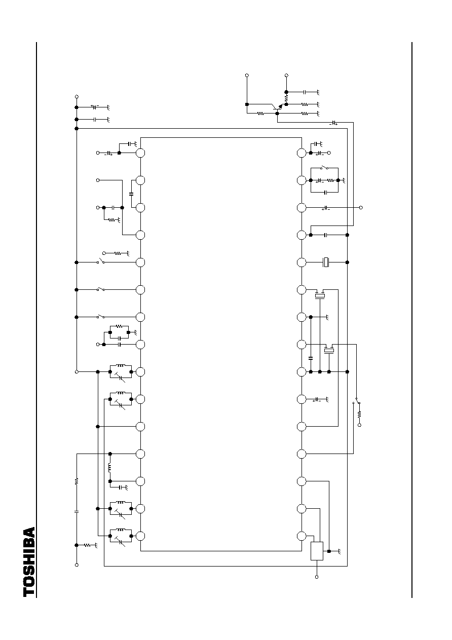
T
A
2154AFN
200
2-
10-
2
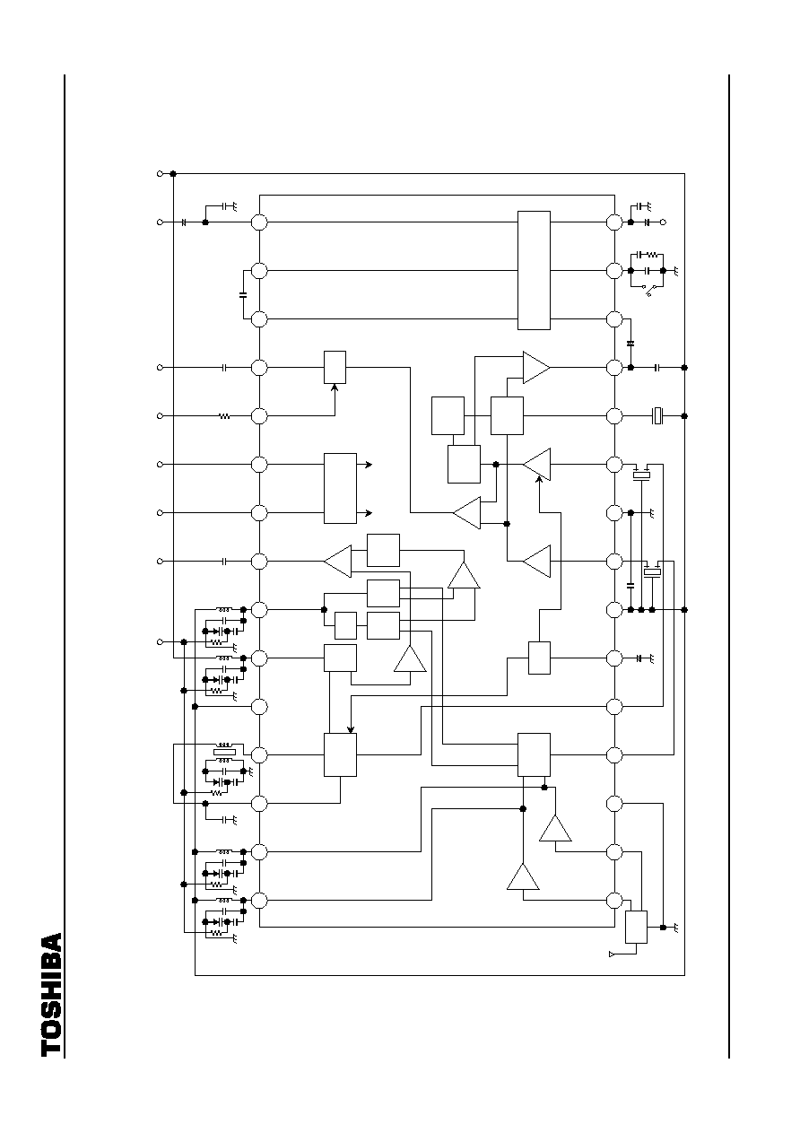
1
2
B
l
ock D
i
agr
a
m
30
TV RF
OUT
29
28
27
26
25
24
23
22
21
20
19
18
17
16
1
2
3
4
5
6
7
8
9
10
11
12
13
14
15
FM RF
OUT
AM
BYPA
SS
AM RF
IN
RFV
CC
AM OS
C
TV FM OSC
OSC OUT
MODE
2
MODE
1
IF RE
Q
IF CO
UN
T
LPF2B
LPF2
A
L OUT
TV RF
IN
FM RF
IN
RF GND
FM MIX
AM MI
X
AGC
V
CC
FM IF IN
GND
AM IF
IN
QUAD
DE
T OUT
MPX IN
LPF1
R OUT
FM
IF
V
T
OS
C
OUT
MO
D
E
SW
2
MO
D
E
SW
1
IF
RE
Q
IF
OUT
L OUT
V
CC
R OUT
MO
N
O
STER
EO
BPF
SW
FM
/AM
/
TV
PW
SW
BUF
F
1/
8 or
1/
16
TV
OS
C
FM
OS
C
1/
2
AM
OS
C
AM
MI
X
BUF
F
FM
/TV
MI
X
BUF
F
AM
IF
AF
IF
B
U
FF
FM
DE
T
AM
DE
T
LE
V
E
L
DE
T
AG
C
FM
M
P
X
FM
RM
TV
RF
TA2154AFN
2002-10-21
3
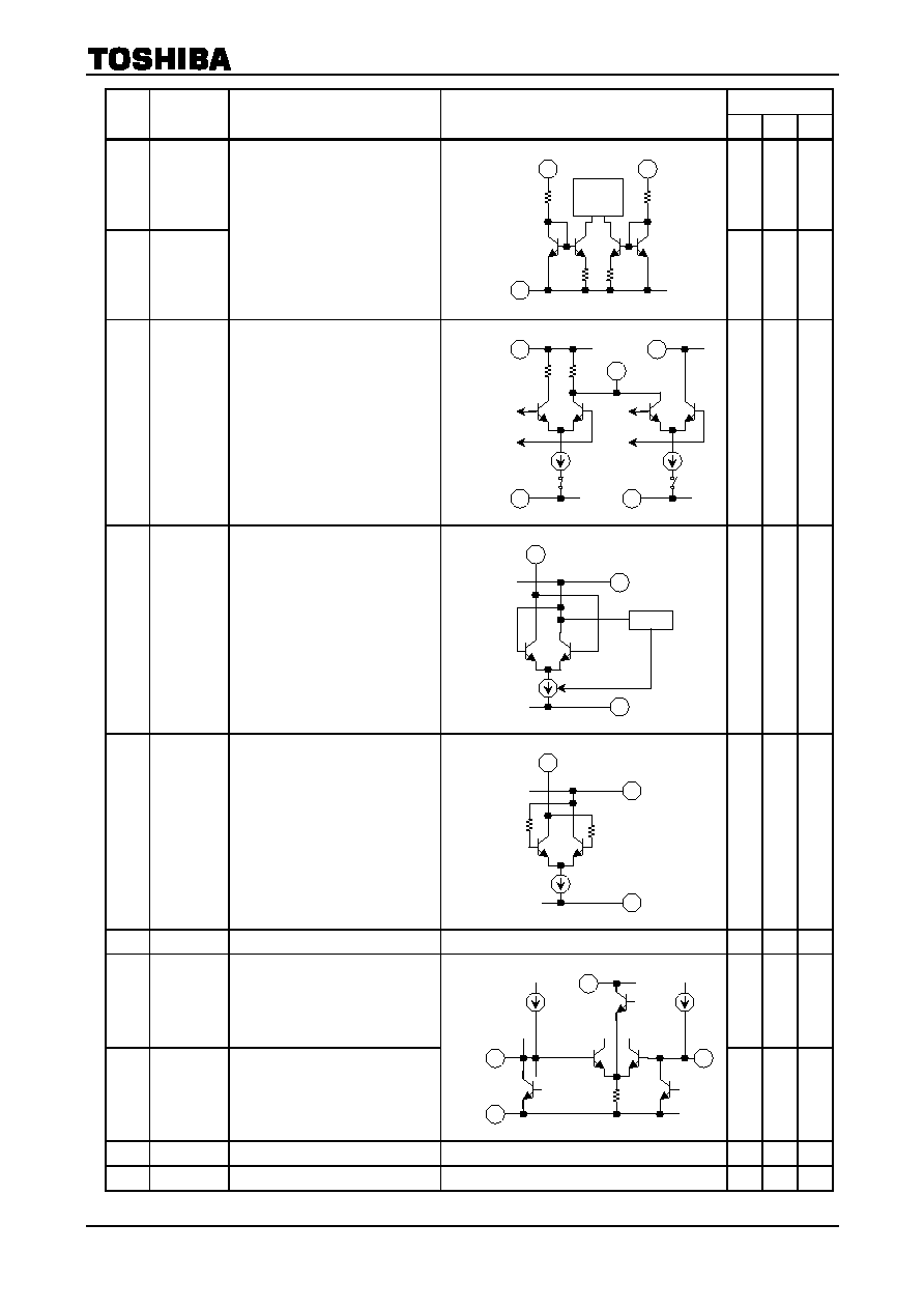
Explanation of Terminals
Terminal voltage: Typical terminal voltage at no signal with the test circuit (V
CC
= 1.2 V, Ta = 25∞C)
Terminal Voltage
Pin
No.
Name Function
Internal
Circuit
AM FM
TV
1
TV RF IN
Input of TV RF signal
0 0
0.1
2
FM RF IN
Input of FM RF signal
0 0.1
0
3
RF-GND
GND (GND for TV/FM stage)
æ
0
0
0
4
FM MIX
Output of TV/FM signal
æ
0.5
0.5
5
AM MIX
Output of AM IF signal
0.6
æ
æ
6 AGC
AGC
∑
AGC time constant is determined
by external capacitor
0 0
0
7 V
CC
V
CC
(V
CC
for AM, FM IF, MPX stage)
æ
1.2
1.2
1.2
3
2
29
100
9
60 pF
FM RF OUT
RF GND
3
1
30
100
9
60 pF
TV RF OUT
RF GND
3
4
TV/FM MIX
7
RF GND
220
W
V
CC
5
AM MIX
7
14 k
W
V
CC
14 k
W
9
GND
3 k
W
6
IF
FM AM

TA2154AFN
2002-10-21
4
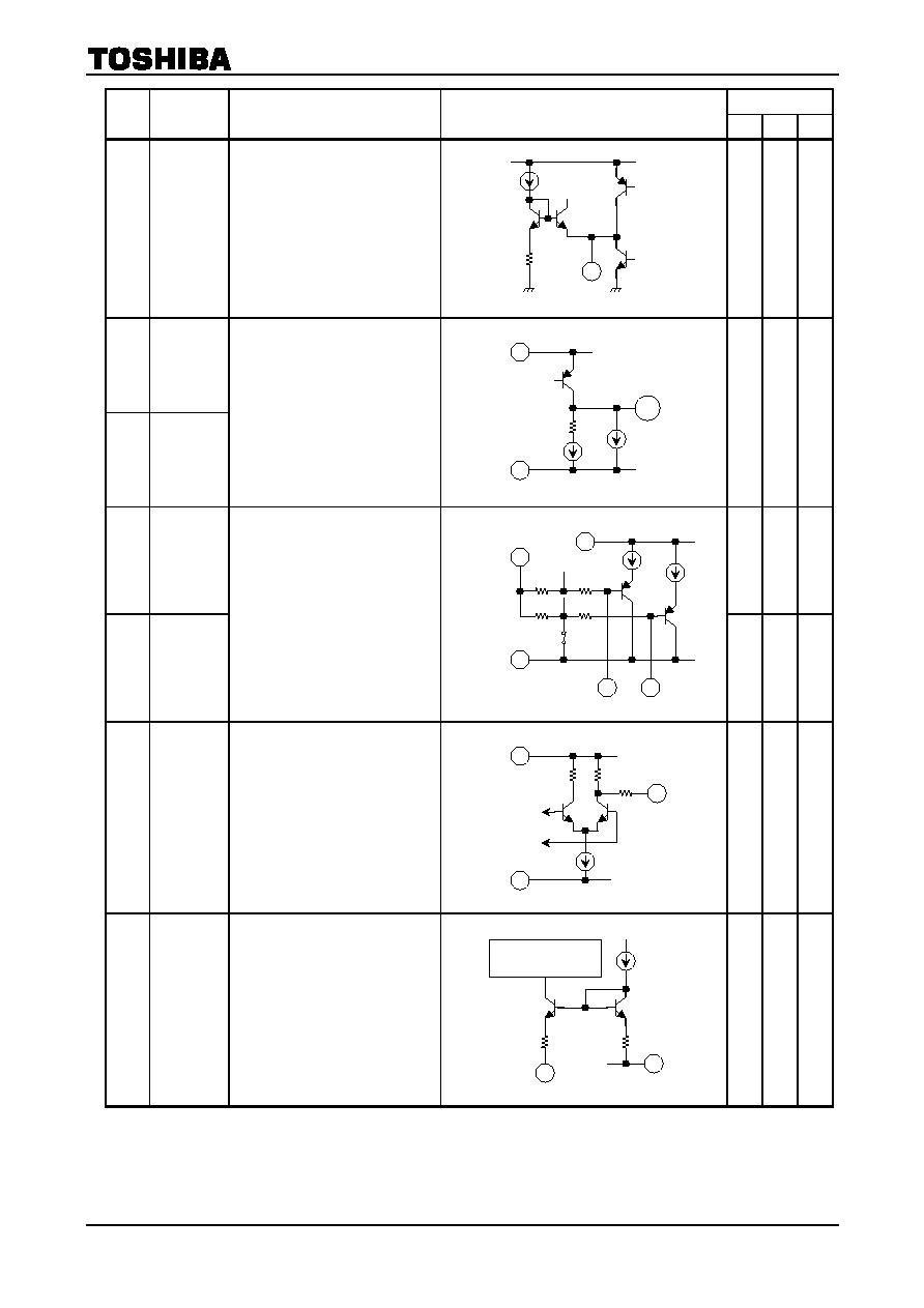
Terminal Voltage
Pin
No.
Name Function
Internal
Circuit
AM FM
TV
8 FM
IF
IN
Input of FM IF signal
Input impedance: 330
W
(typ.)
æ
0.7
0.7
9 GND
GND
(GND for AM, FM IF, MPX stage)
æ
0
0
0
10 AM
IF
IN
Input of AM IF signal
Input impedance: 3 k
W
(typ.)
1.2 1.2
1.2
11 QUAD
FM
QUAD
detector
1.2 1.1
1.1
12 DET
OUT
Detector output
Output impedance
AM:
4
k
W
(typ.)
FM:
500
W
(typ.)
0.6 0.8
0.8
13
MPX IN
Input of MPX
0.1 0.1
0.1
7
V
CC
9
8
330
W
GND
7
V
CC
9
10
GND
3 k
9
3 k
9
7 V
CC
11
1 k
9
9 GND
7 V
CC
9
12
500
W
3.5 k
W
34 k
W
AM DET
FM DET.
7 V
CC
13
5 k
9
9 GND
41 k
W
3.
4 k
9
58.5 k
W
TA2154AFN
2002-10-21
5
Terminal Voltage
Pin
No.
Name Function
Internal
Circuit
AM FM
TV
14 LPF1
LPF terminal for PLL phase
detection.
Connecting this terminal to GND
sets the IC to forced Monaural
mode.
æ
æ
æ
15 R
OUT
16 L
OUT
Output of Stereo signal
0.5 0.5
0.5
17 LPF2A
æ
æ
æ
18 LPF2B
LPF terminals for synchronous
detector
æ
æ
æ
19 IF
COUNT
Output of IF count signal
AM:
450
kHz
FM: 10.7 MHz
1.2 1.2
1.2
20 IF
REQ
IF
request
switch
æ
æ
æ
14
7
V
CC
18
17
39 k
W
100 k
W
13
39 k
W
100 k
W
9
GND
9
GND
500
9
2.
4 k
9
20
Request sensitivity
controller
7
V
CC
10 k
9
9
15/16
7
V
CC
9
GND
2 k
9
2 k
9
19
100
W
TA2154AFN
2002-10-21
6
Terminal Voltage
Pin
No.
Name Function
Internal
Circuit
AM FM
TV
21 MODE1
æ
1.2
1.2
22 MODE2
Mode switch
MODE1
MODE2
Standby: OPEN OPEN
AM: OPEN
V
CC
FM: V
CC
OPEN
TV: V
CC
V
CC
1.2
æ
1.2
23
OSC OUT
Local oscillation buffer output
1.0 1.0
1.0
24 TV/FM
OSC
TV/FM
OSC
1.2 1.2
1.2
25
AM OSC
AM OSC
1.2 1.2
1.2
26 RFV
CC
V
CC
for TV/FM F/E stage
æ
æ
æ
æ
27
AM RF IN
Input of AM RF signal
0.9
æ
æ
28
AM
BYPASS
Referential voltage bypass terminal
for AM RF
0.9
æ
æ
29
FM RF OUT FM RF turning circuit
Cf. pin 2
1.2
1.2
1.2
30
TV RF OUT TV RF turning circuit
Cf. pin 1
1.2
1.2
1.2
21
40 k
9
22
MODE
SW
40 k
9
2 k
9
2 k
9
9
FM
PSC
26
RFV
CC
3
RF GND
1 k
9
1 k
9
23
AM
PSC
7
V
CC
9
GND
V
CC
200
9
25
7
200
9
GND
9
7
V
CC
9
GND
1 k
9
27
28
AGC
AGC
AGC
RFV
CC
24
26
RF GND
3
ALC
TA2154AFN
2002-10-21
7
Application Note
1. Mode switch
The IC controls the mode using pins 21 and 22. Switch conditions by modes are as listed below:
MODE1 (pin 21)
MODE2 (pin 22)
Standby OPEN
OPEN
AM OPEN
V
CC
FM V
CC
OPEN
TV V
CC
V
CC
To change mode, a 10 mA (typ.) current must flow from the IC to the pin connected to V
CC
. When the pin is
open, set the pin voltage to 0.2 V or less (typ.).
2. Forced monaural switch
Forced monaural switch over is done by pin 14.
In case of the electrical switch over by transistor, set up V
CE
(saturation voltage between collector and emitter) 100 mV or less,
otherwise there are some cases that it does not become forced
monaural (VCO STOP) mode.
3. IF count output
To output the signal for IF count, connect IF REQ (pin 20) to GND via R
SEN
and input the IF count
sensitivity or larger.
Switch Condition
MODE1 MODE2 IF
REQ
Output Frequency
Output Voltage
Output
Impedance
AM OPEN
V
CC
450
kHz
180
mVp-p
FM V
CC
OPEN
10.7
MHz
190
mVp-p
TV V
CC
V
CC
Grounded via
R
SEN
10.7 MHz
190 mVp-p
2 k
W
4. Constant of LPF
Caputer range and Lock range is decided by constant of LPF, pin 14, 17, 18.
Care should be taken in changing constant of LPF. Otherwise there are some cases that stereo
characteristics may worse or IC may not operate stereo mode.
5. TV/FM local oscillator
This IC uses the same oscillator for TV and FM. The circuit structure is shown below. In TV mode, the IC
inputs the local oscillator frequency to the mixer as-is. In FM mode, the IC halves the local oscillator
frequency then inputs it to the mixer. This is how the IC receives TV and FM band frequencies.
V
CC
14
V
CE (sat)
When TV is on
24
23
OSC
1/2
divider
TV
MIX
FM
MIX When FM is on
TV
FM
1/4
divider
1/4
divider
BUFF
TA2154AFN
2002-10-21
8
Maximum Ratings
(Ta
=
=
=
=
25∞C)
Characteristics Symbol
Rating
Unit
Supply voltage
V
CC
4.5 V
Power dissipation
P
D
(Note 2)
550
mW
Operating temperature
T
opr
-
10~60 ∞C
Storage temperature
T
stg
-
55~150 ∞C
Note 2: Derated above Ta
=
25∞C in the proportion of 4.4 mW/∞C.
Electrical Characteristics
Unless otherwise specified
: V
CC
=
=
=
=
1.2 V, Ta
=
=
=
=
25∞C, FM F/E: f
=
=
=
=
98 MHz, f
m
=
=
=
=
1 kHz,
D
D
D
D
f
=
=
=
=
±
±
±
±
75 kHz, V
in
=
=
=
=
60dB
m
m
m
m
V EMF
FM IF: f
=
=
=
=
10.7 MHz, f
m
=
=
=
=
1 kHz,
D
D
D
D
f
=
=
=
=
±
±
±
±
75 kHz, V
in
=
=
=
=
80dB
m
m
m
m
V EMF
AM: f
=
=
=
=
1000 kHz, f
m
=
=
=
=
1 kHz, MOD
=
=
=
=
30%, V
in
=
=
=
=
60dB
m
m
m
m
V EMF
MPX: f
m
=
=
=
=
1 kHz, f
p
=
=
=
=
19 kHz
Characteristics Symbol
Test
Circuit
Test Condition
Min
Typ.
Max
Unit
I
CC1
æ
PW
SW
off
20
m
A
I
CC2
æ
AM mode, V
in
=
0
5.0
7
I
CC3
æ
FM mode, V
in
=
0
13.0
17
Supply current
I
CC4
æ
TV mode, V
in
=
0
13.5
17
mA
Input limiting voltage
V
in (lim)
æ
Point where detection output is
-
3dB with Vin
=
60dB
m
V EMF
as reference
æ
12
æ
dB
m
V
EMF
FM
F/E
Local OSC buffer output
voltage
V
osc
(Buff) FM
æ
f
osc
=
6.79375 MHz
(217.4 MHz divided by 32)
150 200
æ
mVp-p
Input limiting voltage
V
in (lim)
æ
Point where detection output is
-
3dB with V
in
=
60dB
m
V EMF
as reference
14
dB
m
V
EMF
TV
F/E
Local oscillator buffer output
V
osc
(Buff) TV
æ
f
osc
=
26.3375 MHz
(210.7 MHz divided by 8)
150 200 mVp-p
Input limiting voltage
V
in (lim)
æ
Point where detection output is
-
3dB with V
in
=
80dB
m
V EMF
as reference
37 42 47
dB
m
V
EMF
Recovered output voltage
V
OD (FM)
æ
æ
115 140 180
mVrms
Signal to noise ratio 1
S/N (FM)
æ
æ
æ
73
æ
dB
Total harmonic distortion 1
THD (FM)
æ
æ
æ
0.2
æ
%
AM rejection ration
AMR (FM)
æ
MOD
=
30%
æ
62
æ
dB
IF count output voltage
V
IF (FM)
æ
æ
150
190
æ
mVp-p
FM
IF
IF count sensitivity
IF
SENS (FM)
æ
R
SEN
=
3.3 k
W
48 53 58
dB
m
V
EMF
Gain G
v
æ
V
in
=
32dB
m
V
EMF
19 29 51
mVrms
Recovered output voltage
V
OD (AM)
æ
æ
27 40 54
mVrms
Signal to noise ratio 2
S/N (AM)
æ
æ
æ
37
æ
dB
Total harmonic distortion 2
THD (AM)
æ
æ
æ
13
æ
%
Local OSC buffer output
voltage
V
osc
(Buff) AM
æ
f
osc
=
14.5 MHz
130
180
æ
mVp-p
IF count output voltage
V
IF (AM)
æ
æ
140
180
æ
mVp-p
AM
IF count sensitivity
IF
SENS (AM)
æ
R
SEN
=
3.3 k
W
27 32 37
dB
m
V
EMF
TA2154AFN
2002-10-21
9
Characteristics Symbol
Test
Circuit
Test Condition
Min
Typ.
Max
Unit
Input resistance
R
IN
æ
æ
æ
26
æ
Output resistance
R
OUT
æ
æ
æ
10
æ
k
W
Voltage gain
G
v
æ
-
2.5
-
0.5
+
1.5
dB
Channel balance
C.B.
æ
V
in
=
150 mVrms (MONO)
-
2.0 0
+
2.0
dB
Max composite signal input
level
V
in (max)
æ
L
+
R
=
90%, P
=
10%,
THD
=
3%
æ
250
æ
mVrms
f
m
=
100 Hz
æ
40
æ
f
m
=
1 kHz
30
40
æ
Separation SEP.
æ
L
+
R
=
135 mVrms,
P
=
15 mVrms
f
m
=
10 kHz
æ
40
æ
dB
MONO THD
(MONO)
æ
V
in
=
150 mVrms (MONO)
æ
0.2
æ
Total harmonic
distortion
ST THD
(ST)
æ
L
+
R
=
135 mVrms,
P
=
15 mVrms
æ
0.4
æ
%
ON ST
(ON)
æ
æ
5.7 8.5
mVrms
ST indicator
sensitivity
OFF ST
(OFF)
æ
æ
1.0 3.2
æ
mVrms
Stereo indicator hysteresis
V
H
æ
To indicator turn OFF from turn
ON
æ
2.5
æ
mVrms
Capture range
C.R.
æ
P
=
15 mVrms
æ
14
æ
%
MPX
Signal to noise ratio
S/N3
æ
V
in
=
150 mVrms (MONO)
æ
70
æ
dB
T
A
2154AFN
200
2-
10-
2
1
10
T
est
C
i
rcu
i
t
AM
R
F
IN
BPF
:
G
T
VS0
5
So
sh
in
Ele
c
tr
i
c
C
o
.,
L
t
d
.
C
F
1
:
SFE1
0
.
7
M
A5
M
u
r
a
ta
C
o
. L
t
d
.
CF2:
P
F
S
450
A
M
u
r
a
ta
C
o
. L
t
d
.
CR:
CDA
L
A
10M
7GA
113
-
BO
M
u
r
a
ta
C
o
. L
t
d
.
30
TV RF
OUT
29
28
27
26
25
24
23
22
21
20
19
18
17
16
1
2
3
4
5
6
7
8
9
10
11
12
13
14
15
FM RF
OUT
AM
BYPA
SS
AM RF
IN
RFV
CC
AM OS
C
TV FM OSC
OSC OUT
MODE
2
MODE
1
IF RE
Q
IF
COUNT
LPF2B
LPF2
A
L OUT
TV RF
IN
FM RF
IN
RF GND
FM MIX
AM MI
X
AGC
V
CC
FM IF IN
GND
AM IF
IN
QUAD
DE
T OUT
MPX IN
LPF1
R OUT
RF
V
CC
OS
C
OUT
MO
D
E
SW
IF
RE
Q
IF
OUT
fv
co
V
CC
R OUT
PH
AS
E
BPF
10 pF
1 k
W
L OUT
0.
022
m
F
2 k
W
75
W
V
CC
RF
V
CC
0.033
m
F
2.
7 m
H
0.01
m
F
MODE
2
MODE
1
3.3 k
W
22 k
W
0.01
m
F
4.7
m
F
4700 pF
4.7
m
F
4700 pF
0.47
m
F
1 k
W
0.068
m
F
MP
X
I
N
10
m
F
680 pF
CR
CF2
270
W
FM
IF
IN
4.7
m
F
TV/
F
M
RF
I
N
0.
1
m
F
PIL
O
T
68 k
W
2.2 k
W
0.022
m
F
2.2
m
F
DE
T
OUT
V
CC2
=
5 V
2.
4 k
W
68 k
W
MO
N
O
/
S
T
GND/
OP
E
N
fv
co
MO
N
L
3
T
1
L
1
L
2
CF1
T
A
215
4AFN
0.033
m
F
220
m
F
0.
033
m
F
TA2154AFN
2002-10-21
11
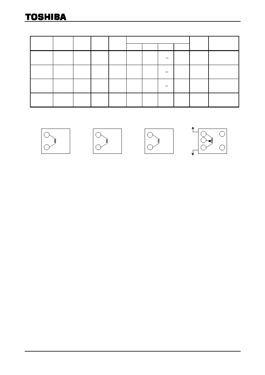
Coil Data
Turns
Coil
Test
Frequency
L
(
m
H)
Co
(pF)
Q0
1-2 2-3 1-3 4-6
Wire
(mm
f
)
L
1
FM RF
100 MHz
æ
æ
79
æ
æ
2
1
2
æ
0.16UEW TOKO
666SNF-305NK
L
2
TV RF
100 MHz
æ
æ
73
æ
æ
4
1
1
æ
0.16UEW
TOKO
666SNF-381NK
L
3
TV/FM
OSC
100 MHz
æ
æ
73
æ
æ
4
1
1
æ
0.16UEW TOKO
666SNF-381NK
T
1
AM OSC
796 kHz
268
æ
65 19 95
æ
æ
0.05UEW
TOKO
5PNR-4957Y
3
1
L
1
: FM RF
3
1
L
2
: TV RF
T
1
: AM OSC
3
1
2
4
6
V
CC
Pin 25
3
1
L
3
: TV/FM OSC
(BOTTOM VIEW)

TA2154AFN
2002-10-21
12
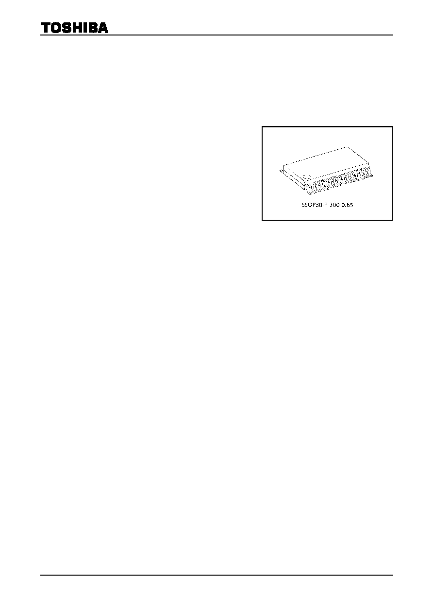
Package Dimensions
Weight: 0.17 g (typ.)

TA2154AFN
2002-10-21
13
∑
TOSHIBA is continually working to improve the quality and reliability of its products. Nevertheless, semiconductor
devices in general can malfunction or fail due to their inherent electrical sensitivity and vulnerability to physical
stress. It is the responsibility of the buyer, when utilizing TOSHIBA products, to comply with the standards of
safety in making a safe design for the entire system, and to avoid situations in which a malfunction or failure of
such TOSHIBA products could cause loss of human life, bodily injury or damage to property.
In developing your designs, please ensure that TOSHIBA products are used within specified operating ranges as
set forth in the most recent TOSHIBA products specifications. Also, please keep in mind the precautions and
conditions set forth in the "Handling Guide for Semiconductor Devices," or "TOSHIBA Semiconductor Reliability
Handbook" etc..
∑
The TOSHIBA products listed in this document are intended for usage in general electronics applications
(computer, personal equipment, office equipment, measuring equipment, industrial robotics, domestic appliances,
etc.). These TOSHIBA products are neither intended nor warranted for usage in equipment that requires
extraordinarily high quality and/or reliability or a malfunction or failure of which may cause loss of human life or
bodily injury ("Unintended Usage"). Unintended Usage include atomic energy control instruments, airplane or
spaceship instruments, transportation instruments, traffic signal instruments, combustion control instruments,
medical instruments, all types of safety devices, etc.. Unintended Usage of TOSHIBA products listed in this
document shall be made at the customer's own risk.
∑
The products described in this document are subject to the foreign exchange and foreign trade laws.
∑
The information contained herein is presented only as a guide for the applications of our products. No
responsibility is assumed by TOSHIBA CORPORATION for any infringements of intellectual property or other
rights of the third parties which may result from its use. No license is granted by implication or otherwise under
any intellectual property or other rights of TOSHIBA CORPORATION or others.
∑
The information contained herein is subject to change without notice.
000707EBA
RESTRICTIONS ON PRODUCT USE