TA32305FN/FNG
2003-12-04
1
TOSHIBA Bipolar Linear Integrated Circuit Silicon Monolithic
TA32305FN/TA32305FNG*
RF 1chip Receiver and Transmitter for low power wireless
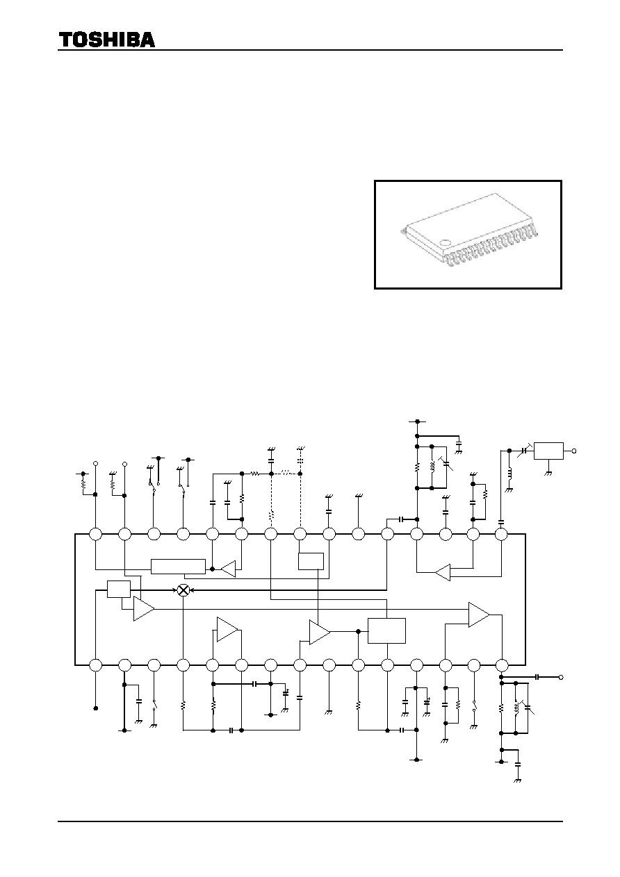
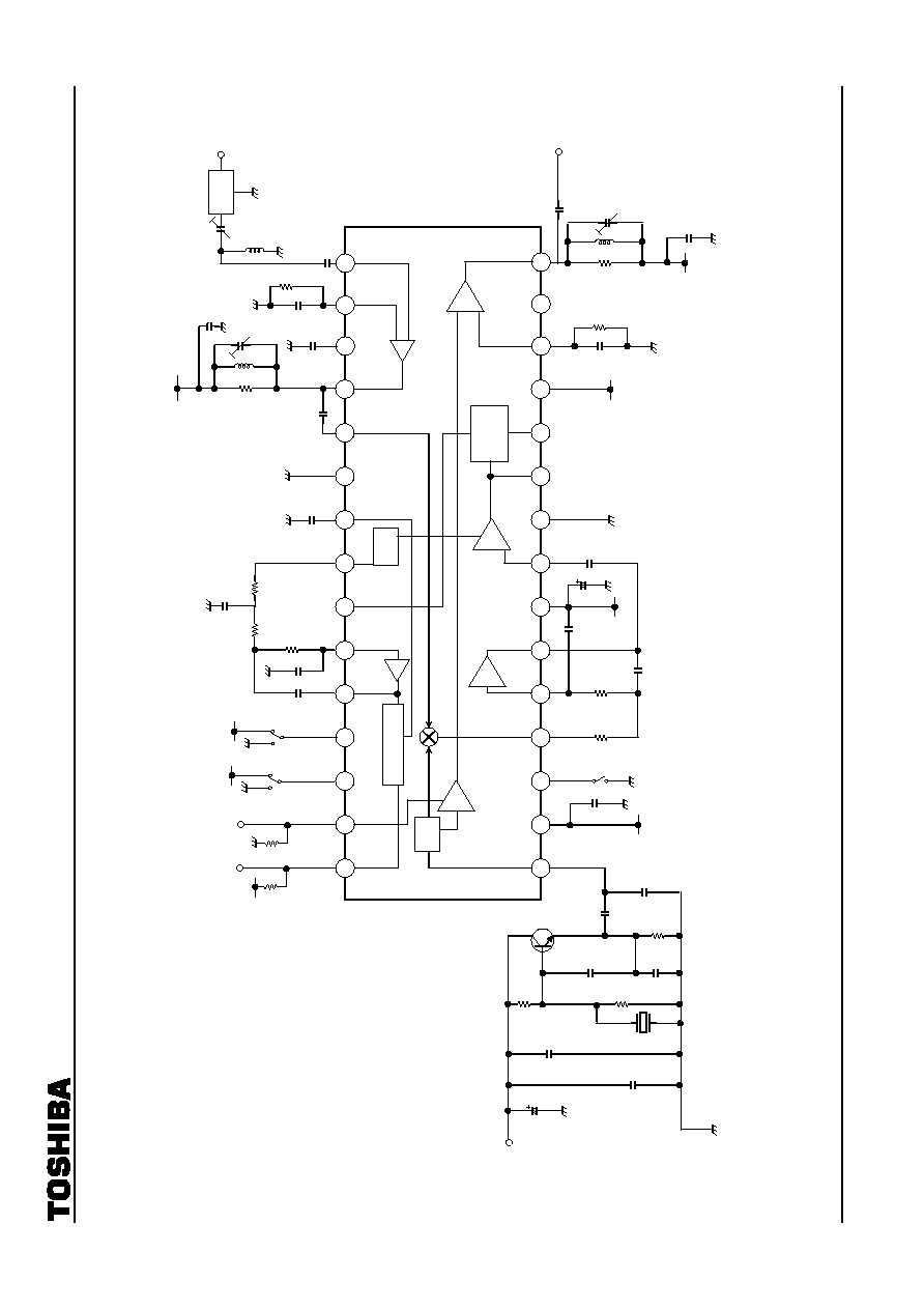
The TA32305FN is an RF 1 chip receiver and transmitter IC.
Receiver is for AM/FM radio.
The IC incorporates an RF amp, 2-level comparator, and local
◊8 circuit.
This IC's main use is remote control.
Features
∑
RF frequency: 240 to 450 MHz (multiplication is used)
∑
IF frequency: 80 kHz
∑
Operating voltage range: 2.2 to 5.5 V
∑
Current dissipation: TX 4.3 mA/ RX 5.6 mA (FM), 5.3 mA (AM)
(except current at oscillator circuit)
∑
Current dissipation at BS: 0 µA (typ.)
∑
Small package: 30-pin SSOP (0.65 mm pitch)
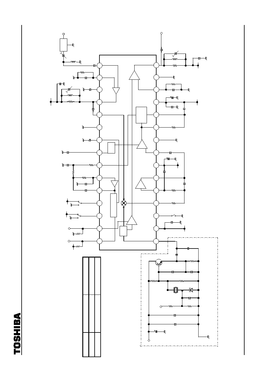
Block Diagram
*: TA32305FNG Package is Pb-Free.
SSOP30-P-300-0.65
Weight: 0.17 g (typ)
12
4
3
5
6
7
8
10
11
19
27
28
26
25
24
23
22
21
20
◊
8
RSSI
REF
AF
OUT
MIX
IN
GND1
RF
DEC
CHARGE
RF
IN
Vcc3
IF IN GND2
IFF
OUT
MIX
OUT
U/L
IFF
IN
OSC
IN
RF
OUT
29
30
2
1
TX LPF
OUT
LPF
IN
Detector
IF
OUT QUAD
Vcc2
V
CC
1
9
18
13
17
14
15
16
TX
Power
AM/
FM
TX
OUT
RX
TX
DATA
RX
DATA
Comparator
RSSI
SAW
TA32305FN/FNG
2003-12-04
2
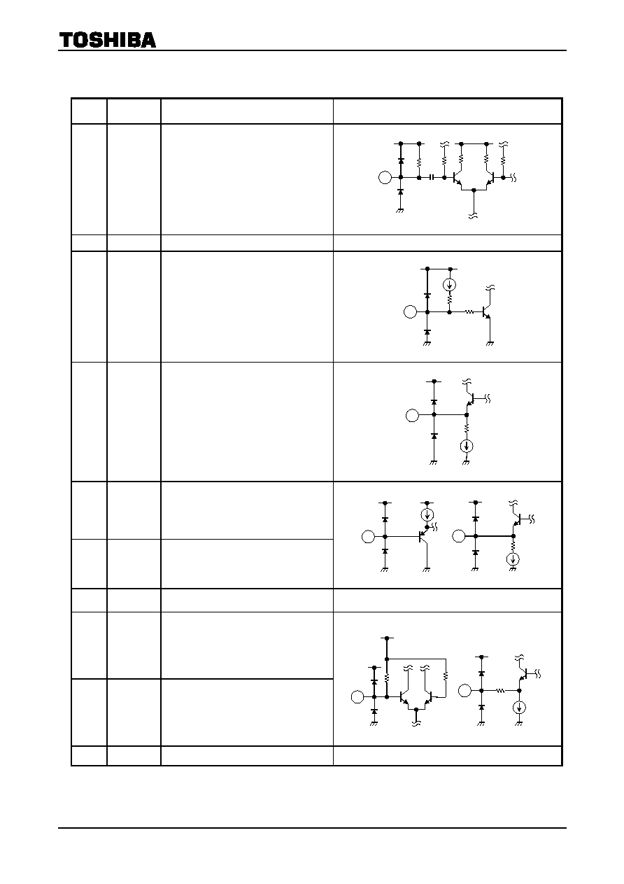
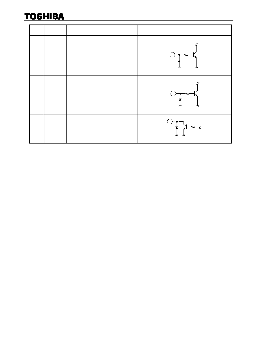
Pin Description
(the values of resistor and capacitor in the internal equivalent circuit are typical.)
Pin No.
Pin Name
Function
Internal Equivalent Circuit
1
OSC IN
Local oscillator input pin.
2 V
CC
1
Local' power supply pin.
3 U/L
U/L switch pin.
OPEN : Upper Local
L : Lower Local
Do not connect Vcc.
4 MIX
OUT
Mixer output pin.
The output impedance of the pin is typically
225
.
5
IFF IN
IF filter input pin.
6
IFF OUT
IFfilter output pin.
7 V
CC
2
Power supply pin 2.
8
IF IN
IF amp input pin.
10
IF OUT
IF amp output pin.
9
GND2
GND pin 2.
100 k
3
10 k
8
10k
10k
10
200
2 pF
1
15 k
10 k
10 k
15 k
50 k
200
4
6
100
5
TA32305FN/FNG
2003-12-04
3
Pin No.
Pin Name
Function
Internal Equivalent Circuit
11 QUAD
Phase-shift input terminal for the FSK
Demodulator.
12
Vcc3
Power supply pin 3.
13
TX Power
Regulating TX output power pin.
15
TX OUT
TXsignal output pin.
14 AM/FM
Changeover switch for AM/ FM.
OPEN : AM
L : FM
Do not connect Vcc.
16
RF IN
RF signal input pin.
17
RF DEC
Emitter pin for internal transistor.
19
RF OUT
RF amp output pin.
18 CHARGE
Control terminal for quick charge circuit.
To use the quick charge circuit, attach a
capacitor.
19
17
16
3 k
10 k
120 k
14
10 k
11
10k
32 k
32 k
15
13
18
100 k
5 k
250
TA32305FN/FNG
2003-12-04
4
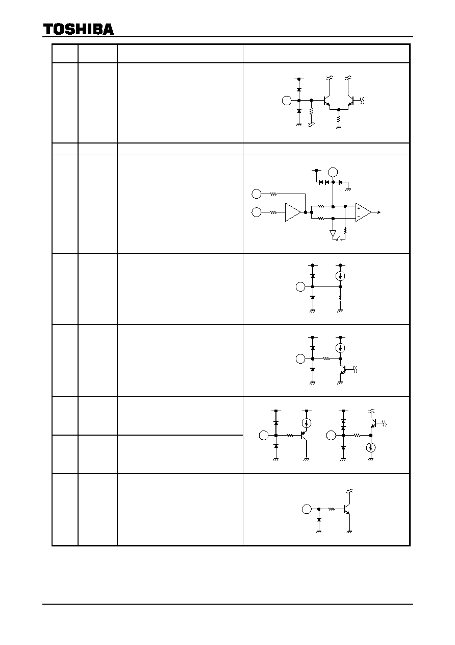
Pin No.
Pin Name
Function
Internal Equivalent Circuit
20 MIX
IN
Mixer input pin.
21
GND1
GND pin 1.
22 REF
Threshold input terminal for 2-level FM/AM
comparator.
23 RSSI
RSSI output pin.
This pin is connected internal circuit.
MONI pin during transmitting.
24
AF OUT
Output terminal for FM demodulator.
25
LPF IN
FM/AM LPF input pin.
26
LPF OUT
FM/AM LPF output pin.
27
TX
Battery saving pin for transmitter.
23
24 k
24
330
41 k
27
25
5 k
26
250
25
26
22
250
5 k
100 k
100 k
DATA
COMP
33 k
20
2.4 k
TA32305FN/FNG
2003-12-04
5
Pin No.
Pin Name
Function
Internal Equivalent Circuit
28
RX
Battery saving pin for receiver.
29 TX
DATA
AM modulation switch for transmitter.
L : Output ON
H : Output FF
30 RX
DATA
FM/AM waveform shaping output pin for
receiver.
Open collector output.
Connect a pull-up resistor.
Equivalent circuits are given to help understand design of the external circuits to be connected. They do not
accurately represent the internal circuits.
2 k
30
30 k
28
97 k
28

TA32305FN/FNG
2003-12-04
6
Functions
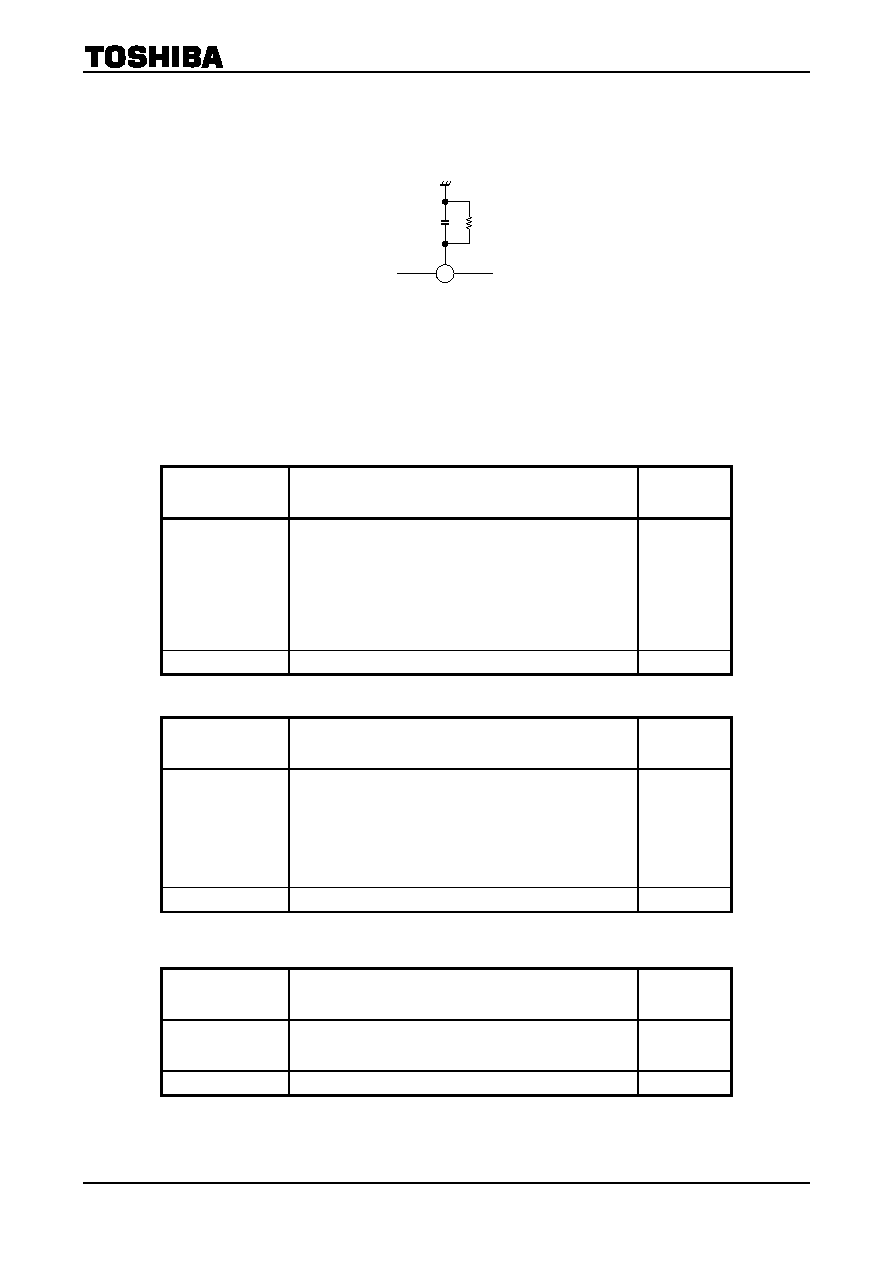
1. Waveform Shaper Circuit (comparator)
The output data (pin 30) are inverted.
2. RSSI Function
DC potential corresponding to the input level of IF IN (pin 8) is output to RSSI (pin 23). Output to
RSSI (pin 23) is converted to a voltage by the internal resistance. Thus, connecting external resistance R
to pin 21 varies the gradient of the RSSI output as shown below. Note that due to the displacement of
temperature coefficients between external resistor R and the internal IC resistor IC resistor, the
temperature characteristic of the RSSI output may change. Also, the maximum RSSI value should be
V
CC
- 0.8 V or less.
Figure 1
Figure 2
3. S Curve Characteristics
Changing external capacitance C27 varies the gradient of the S curve characteristics as shown below.
In case of widening the detection range, heightening IF frequency or lowering demodulation output,
make the gradient of the S curve characteristics gentle less than typical (120pF).
When using this IC by about 2.2V (low supply), set the constant of C27 100pF or add attenuator to AF
OUT (24 pin).
Figure 3
4. V
CC
Pin and GND Pin
Use the same voltage supply for V
CC1
(2 pin) and V
CC2
(7 pin) and V
CC3
(12 pin) (or connect them).
Also, use the same voltage supply source for GND1 (21 pin) and GND2 (9 pin) (or connect them).
5. Local Oscillator Circuit
The local oscillator circuit is external-input-only. The device incorporates no transistor for oscillation.
Input to pin 1 at a level from 92 to 105dB
µV.
Adjust the values of constants C shown in the application circuit diagram so that the input level will
become approximately 100dB
µV.
6. U/L switch pin
It is possible to switch Mixer output frequency to upper local or lower local comparing RF input
frequency.
IF input level
After R is
connected
24 k
23
R
IF frequency
After C is
lessened
TA32305FN/FNG
2003-12-04
7
7. RF Amp Current Adjustment
The RF amp current dissipation can be regulated by varying resistor R as shown in the figure below.
When R
= 560 , the current dissipation is approximately 600 µA.
Figure 4
8. Battery-Saving (BS) Function
The IC incorporates a battery-saving function. These functions offer the following selection.
Receiver
FM Mode (FM/AM pin: GND)
RX Pin
Circuit Status in the IC
IC Current
Dissipation
(at no signal)
H
Circuits in operation:
◊
8 circuit
Mixer
RF amp
Comparator
IF amp
Detector circuit
RSSI
Comparator capacitor charger circuit
5.6 mA (typ.)
L All
circuits
0 mA (typ.)
AM Mode (FM/AM pin: OPEN)
RX Pin
Circuit Status in the IC
IC Current
Dissipation
(at no signal)
H
ircuits in operation:
◊
8 circuit
Mixer
RF amp
Comparator
IF amp
RSSI
Comparator capacitor charger circuit
5.3 mA (typ)
L All
circuits
0 mA (typ)
Transmitter
TX Pin
Circuit Status in the IC
IC Current
Dissipation
(at no signal)
H
Circuits in operation:
◊
8 circuit
TX amp
4.3 mA (typ)
L All
circuits
0 mA (typ)
17
R
RF DEC

TA32305FN/FNG
2003-12-04
8
9.
RF Amp Gain 2
RF amp gain 2 (G
v (RF) 2
) is a reference value calculated as follows. Measure G
RF
in the following figure.
G
v (RF) 2
is calculated as follows:
G
v (RF) 2
= G
RF
- G
v (MIX)
Figure 5
10. Waveform-Shaping Output Duty Cycle
The specified range of electrical characteristics is only available for single-tone.
11. Treatment of FM Terminal when Using AM
When using AM, it is not necessary to treat the QUAD pin (pin 11). Leave it open or connected to an
FM external circuit. To use the bit rate filter, connect the RSSI pin (pin 23) to the bit rate filter through a
resistor. The AF-OUT pin (pin 24) should be left open.
Figure 6
Figure 7
R13
R14
AF
OUT
RSSI
Bit rate filter for FM
C18
C19
24
23
27 nH
1000 pF
4
20
19
16
33 nH
0.01
µ
F
SG
30dB
µ
V
G
RF
6 pF
6 pF
1 k
23
24
R13
AF
OUT
RSSI
Bit rate filter for AM
R15
C18
R
TA32305FN/FNG
2003-12-04
9
12. Control Terminal for Quick Charge Circuit (CHARGE)
CHARGE (18 pin) is control terminal for quick charge circuit. REF (22 pin) control terminal for quick
charge a given period by time constant of internal resistance and outside capacitance. Enabling the
CHARGE pin requires an external capacitor. In normal operation, connect a capacitor having the same
capacitance as that of the capacitor connected to the REF pin (pin 22).
If the connected external capacitor (C30) is 0.1
µF, the quick charge time is 7 ms (typically).
13. Bit Rate Filter for FM
The current FM bit rate filter is used as a tertiary filter.
If the filter is to be used at a rate other than 1200 bps, please change the filter constant.
Quadratic Filter (NRZ)
R12 R13 R14 C14 C15 C18
1200 bps
68 k
68
k
68
k
0.01
µ
F
560 pF
3300 pF
2400 bps
68 k
68
k
68
k
4700 pF
270 pF
1500 pF
4800 bps
68 k
68
k
68
k
2200 pF
150 pF
680 pF
9600 bps
68 k
68
k
68
k
1200 pF
68 pF
390 pF
14. Bit Rate Filter for AM
The current AM bit rate filter is used as a quadratic filter.
If the filter is to be used at a rate other than 1200 bps, please change the filter constant.
Quadratic Filter (NRZ)
(the bit rate filter time constant takes into account the internal resistance RSSI (24 k
))
R15 R12 C14 C15
1200 bps
43 k
68
k
4700 pF
1500 pF
2400 bps
43 k
68
k
2200 pF
680 pF
4800 bps
43 k
68
k
1000 pF
390 pF
9600 bps
43 k
68
k
470 pF
180 pF
In addition, the current AM bit rate filter can be used as a tertiary filter.
If the filter is to be used at a rate other than 1200 bps, please change the filter constant.
Quadratic Filter (NRZ)
(the bit rate filter time constant takes into account the internal resistance RSSI (24 k
)
)
R15 R13 R12 C14 C15 C18
1200 bps
43 k
68
k
68
k
0.01
µ
F
560 pF
3300 pF
2400 bps
43 k
68
k
68
k
4700 pF
270 pF
1500 pF
4800 bps
43 k
68
k
68
k
2200 pF
150 pF
680 pF
9600 bps
68 k
68
k
68
k
1200 pF
68 pF
390 pF
For the cutoff frequency of the bit rate filter, specify a sufficiently high value for the bit rate to be used.
Specifying a relatively high cutoff frequency for the bit rate filter enables a low capacitor to be used at
the REF pin, therefore making the pulse rise quickly.
When AM is used, the internal resistance of RSSI is used. So, take the output resistance into account
when specifying a cutoff frequency.

TA32305FN/FNG
2003-12-04
10
15. Simple Image Cancel Mixer for Receiver
The IC incorporates simple image cancel mixer for receiver.
16. TX Amp Current Adjustment
The RF amp current dissipation can be regulated by varying resistor R as shown in the figure below.
When R
= 560 , the current dissipation is approximately 680 µA..
Figure 8
13
R
TX_POW

TA32305FN/FNG
2003-12-04
11
Cautions for Designing Circuit Board Patterns
Observe the following cautions when designing circuit patterns for this product.
Local Oscillator Circuit (pin 1)
Isolate the local oscillator circuit block sufficiently from the RF amp block.
Isolate the local oscillator circuit block securely so that its output will not get in the IF input, IF filter, or
mixer input.
Do not place the local oscillator circuit block too close to the ceramic filter.
Subdivide the ground pattern for the local oscillator circuit block, and connect the subdivisions with thin
lines.
IF Input and Output Block (pin 8, 10)
Isolate the input from output patterns of the IF filter and detector block securely from each other.
Demodulator Circuit Block (pin 11)
Isolate the demodulator circuit block sufficiently from the IF input block (pin 8).
Do not place the LC too close to the IC device.
Data Output Block (pin 30)
Isolate the data output block sufficiently from the IF input block (pin 8).
Isolate the output pattern of the data output block from other circuits as much as possible, so any noise from
a stage subsequent to the output will not affect them.
RF Amp Circuit Block
1)
Preventing RF amp oscillation
Do not place the patterns connected to pins 16 and 17 too close to each other.
Isolate the patterns connected to the input block (pin 16) and output block (pin 19) from each other.
Make the RF input signal line relatively thin.
Place a relatively wide ground pattern between the RF-IN pin (pin 16) and RF-DEC pin (pin 17).
Connect the RF-OUT pin (pin 19) and MIX-IN pin (pin 20) with the shortest possible pattern.
2)
Attaining a sufficient gain
To attain a sufficient RF amp gain, select an optimum value for the input matching circuit block (pin 16)
according to the board circuit pattern.
3)
Sharing antenna with receiver and transmitter
Using hi power application, place the patterns connected to SAW filter and pin 15 close.
IC Mounting Area
Provide a ground pattern under the IC device, and prepare relatively many through holes.
Cautions for mounting
Mount better accurate constants of capacitance in IF filter block and detector block.

TA32305FN/FNG
2003-12-04
12
Maximum Ratings
(unless otherwise specified, Ta
=
25∞C. the voltage is with reference to the ground level.)
Characteristics Symbol
Rating
Unit
Supply voltage
V
CC
6 V
Power dissipation
P
D
860 mW
Operating temperature range
T
opr
-
40~85
∞C
Storage temperature range
T
stg
-
55~150 ∞C
The maximum ratings must not be exceeded at any time. Do not operate the device under conditions outside the
above ratings.
Operable Range
(unless otherwise specified, Ta
=
25∞C. the voltage is with reference to the ground level.)
Characteristics Symbol
Test
Circuit
Test Condition
Min
Typ.
Max
Unit
Operating voltage range
V
CC
2.2 3.0 5.5 V
RF operating frequency
f
RF
250
450
MHz
Operating ranges indicate the conditions for which the device is intended to be functional even with the electrical
changes.
Electrical Characteristics
(unless otherwise specified: Ta
=
25∞C, V
CC
=
3 V, U/L
=
OPEN,
fin (RF)
=
fin (MIX)
=
314.96 MHz, fin (IF)
=
80 kHz))
Receiver Block
Characteristics Symbol
Test
Circuit
Test Condition
Min
Typ.
Max
Unit
Current dissipation at battery saving
I
cco
3
RX
=
"L",TX
=
"L"
0 5
µ
A
RF amp gain 1
G
v (RF) 1
1
(5)
The input and output
impedances are 50
.
-9.0 -6.5 -4.0
dB
Mixer conversion gain
G
v (MIX)
18 21 24 dB
RSSI output voltage 1
V
RSSI1
V
in (MIX)
=
25dB
µ
VEMF
in AM mode
0.25 0.5 0.75
V
RSSI output voltage 2
V
RSSI2
V
in (MIX)
=
50dB
µ
VEMF
in AM mode
0.7 1.0 1.3 V
RSSI output voltage 3
V
RSSI3
V
in (MIX)
=
80dB
µ
VEMF
in AM mode
1.35 1.7 2.05
V
RSSI output resistance
R
RSSI
18 24 30 k
Comparator input resistance
R
COMP
75 100 125
k
RX data output voltage (L level)
V
RXDATAL
1 (3) I
RXDATAL
=
200
µ
A
0.04 0.4 V
RX data output leakage current (H level)
I
RXDATAH
1
(4)
0 2
µ
A
RX pin H-level input voltage
V
RXH
2.0
5.5
V
RX pin L-level input voltage
V
RXL
0
0.2 V

TA32305FN/FNG
2003-12-04
13
FM Mode
(Ta
=
25∞C, Vcc
=
3.0 V, fin (RF)
=
fin (MIX)
=
314.96 MHz, U/L
=
OPEN,
fin (IF)
=
80 kHz, dev
=
±
8 kHz, fmod
=
600 Hz ((single wave))
Characteristics Symbol
Test
Circuit
Test Condition
Min
Typ.
Max
Unit
Quiescent current consumption
(for FM)
Iccqfm 2
(1)
RX/FMAM
=
"H/ L"
Fin (Lo)
=
39.38 MHz
4.2 5.6 7.0 mA
Demodulated output level
Vod
V
in (MIX)
=
60dB
µ
VEMF
95 130 165
mVrms
Waveform shaping duty ratio
DRfm 1
(2)
V
in (MIX)
=
60dB
µ
VEMF
For single tone
45 50 55 %
AM Mode
(Ta
=
25∞C, Vcc
=
3.0 V, fin (RF)
=
fin (MIX)
=
314.96 MHz, U/L
=
OPEN,
fin (IF)
=
80 kHz, AM
=
90%, fmod
=
600 Hz (square wave) )
Characteristics Symbol
Test
Circuit
Test Condition
Min
Typ.
Max
Unit
Quiescent current consumption
(for AM)
Iccqam 2
(2)
RX/FMAM
=
"H/ OPEN"
Fin (Lo)
=
39.38 MHz
3.9 5.3 6.7 mA
Reference characteristic data
Dram 1
(2)
V
in (MIX)
=
60dB
µ
VEMF
For single tone
45 50 55 %
Transmitter Block
Characteristics Symbol
Test
Circuit
Test Condition
Min
Typ.
Max
Unit
Quiescent current consumption
(for Transmitter Mode)
Iccqtx
2 (3) TX= "H"
3.0
4.3
5.6
mA
TXDATA pin H-level input voltage
V
TXDATAH
2.0
5.5
V
TXDATA pin L-level input voltage
V
TXDATAL
0
0.2 V
TX pin H-level input voltage
V
TXBSH
2.0
5.5
V
TX pin L-level input voltage
V
TXBSL
0
0.2 V
TXoutput signal level 1
V
TX1
The output impedances are 50
-25.5 -22.5 -19.5
dBm
Reference Characteristic Data
*
Characteristics Symbol
Test
Circuit
Test Condition
Typ.
Unit
RF amp gain 2
G
v (RF) 2
30
dB
RF amp input resistance
R
(RF)
IN
1.0
k
RF amp input capacitance
C
(RF)
IN
2.0
pF
RF amp output capacitance
C
(RF)
OUT
2.0
pF
Mixer input resistance
R
(MIX)
IN
1.2 k
Mixer input capacitance
C
(MIX)
IN
1.6 pF
Mixer intercept point
IP3
96 dB
µ
V
IFamp gain
G
v (RF)
65
dB
Signal-to-noise ratio 1
S/N1 1
(8) V
in (MIX)
=
20dB
µ
VEMF
19 dB
Signal-to-noise ratio 2
S/N2
1 (8)
V
in (MIX)
=
60dB
µ
VEMF
56 dB
TX amp output capacitance
C
(TX)
OUT
2.0 pF
TX output signal level 2
V
TX2
-14 dBm
* :
These characteristic data values are listed just for reference purposes. They are not guaranteed values.

TA32305FN/FNG
2003-12-04
14
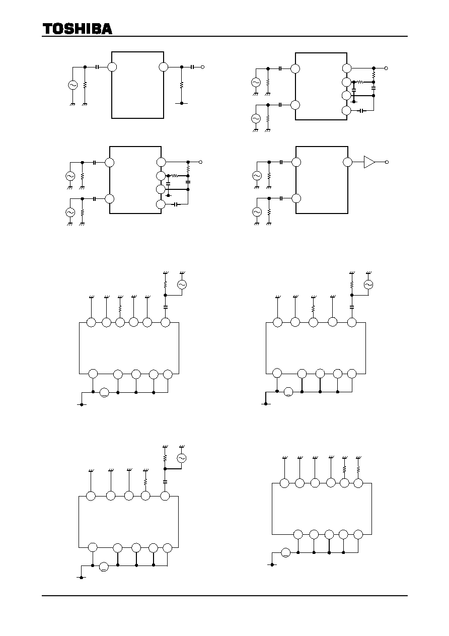
Typical Test Circuit
(FSK)
Test Circuit 1
(1) V
RSSI
(2)
D
R
(3) V
DATA L
(4)
I
DATA H
12
4
3
5
6
7
8
10
11
19
27
28
26
25
24
23
22
21
20
◊
8
RSSI
REF
AF
OUT
MIX
IN
GND1
RF
DEC
CHARGE RF
IN
Vcc3
IF IN GND2
IFF
OUT
MIX
OUT
U/L
IFF
IN
OSC
IN
RF
OUT
29
30
2
1
TX LPF
OUT
LPF
IN
Detector
IF
OUT QUAD
Vcc2
V
CC
1
9
18
13
17
14
15
16
TX
Power
AM/
FM
TX
OUT
RX
TX
DATA
RX
DATA
Comparator
RSSI
SAW
1000 pF
560
R21
C35
1000 pF
C32
0.1
µ
F
C30
C22
V
CC
V
CC
V
CC
V
CC
V
CC
V
CC
V
CC
V
CC
27nH
1 k
L1
R19
6 pF
0.01
µ
F
C24
C25
1000 pF
C26
C22 0.1
µ
F
68 k
R13
0.01
µ
F
560 pF
68 k
C14
C15
R12
100 k
R7
100 k
R6
0.1
µ
F
C12
R10 4.3
k
4.7 k
R11
R18 20
k
560
R20
R22
560
C13
120 pF
10
µ
F
C17
10
µ
F
0.1
µ
F
1000
p
F
C28
C29
C31
C27
120 pF
L2
0.01
µ
F
1000 pF
C16
L3
33 nH
C36 5 pF
R14
68 k
C19 1000
pF
C18 3300
pF
6 pF
C37
C20 330
pF
C33
22nH
6 pF
C34
V
1000 pF
SG
1
51
0.01
µ
F
20
SG
51
1000 pF
23
30
100 k
V
CC
SG
1
51
0.01
µ
F
20
SG
51
1000 pF
30
V
R
=
100 k
25
22
1.5 V
V
V
2.0 V
25
22
2.0 V
V
V
1.5 V
30
V
CC
I
=
V/100
◊
10
3
V
100 k
TA32305FN/FNG
2003-12-04
15
(5) G
v (RF) 1
(6)
G
v (MIX)
(7) G
v (MIX) vs
V
LO
(8)
S/N1,
2
Test Circuit 2
(1) I
ccqfm
(2) I
ccqam
Test Circuit 3
(3) I
cctx
I
cco
SG
16
19
51
1000 pF
1000 pF
SG
1
26
51
0.01
µ
F
20
SG
51
1000 pF
Buff
9
SG
560
1
17
14
51
0.01
µ
F
27
21
12 19
A
2
28
7
Vcc
9
SG
560
1
12 19
A
17
51
0.01
µ
F
2
21
28
7
27
V
CC
SG
560
1
13
51
0.01
µ
F
28
21
12 15
A
2
27
7
V
CC
9
560
V
CC
17
12
19
A
21
28
2
7
15
27
560
13
4
SG
1
51
0.01
µ
F
20
SG
51
1000 pF
5
6
8
4.7 k
330 pF
1000 pF
120 pF
4
SG
1
51
0.01
µ
F
20
SG
51
1000 pF
5
6
8
4.3 k
4.7 k
330 pF
1000 pF
120 pF
TA32305FN/FNG
2003-12-04
16
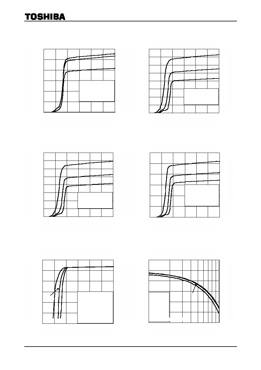
Reference Data
(This is characteristics data when it used evaluation boards. This is not
guarantee on condition that it is stating except electrical characteristics.)
Quiescent Current Consumption ≠
Supply Voltage Characteristics
Supply voltage V
CC
(V)
Quiescent curren
t
consumption
I
CC
(
m
A
)
Quiescent Current Consumption ≠
Supply Voltage Characteristics TX Mode
Supply voltage V
CC
(V)
Quiescen
t curr
ent consump
t
ion
I
CCq
tx
(
m
A
)
RF Amp Gain ≠
Supply Voltage Characteristics
Supply voltage V
CC
(V)
RF amp conversi
on gain
(dB)
Quiescent Current Consumption ≠
Supply Voltage Characteristics FM Mode
Supply voltage V
CC
(V)
Quiescen
t curr
ent consump
t
ion
I
CCqfm
(
m
A
)
Quiescent Current Consumption ≠
Supply Voltage Characteristics AM Mode
Supply voltage V
CC
(V)
Quiescen
t curr
ent consump
t
ion
I
CCqam
(
m
A
)
RF Amp Frequency Characteristics
RF IN input frequency f (RF) in (MHz)
RF amp conversi
on gain
(dB)
0
1
2
3
4
5
6
0
1
2
3
4
5
6
BS
f (Lo) in = 39.38 MHz
V (Lo) in = 100dBV
*
FM
AM
TX
0
1
2
3
4
5
6
7
8
0
1
2
3
4
5
6
f (Lo) in = 39.38 MHz
V (Lo) in = 100dBV
*
25
125
-40
0
1
2
3
4
5
6
7
8
0
1
2
3
4
5
6
f (Lo) in = 39.38 MHz
V (Lo) in = 100dBV
*
25
125
-40
0
1
2
3
4
5
6
0
1
2
3
4
5
6
f (Lo) in = 39.38 MHz
V (Lo) in = 100dBV
-40
125
25
-60
-50
-40
-30
-20
-10
0
0
1
2
3
4
5
6
f(RF)in=314.96MHz
V(RF)in=50dBuV
<Meas Point>
RFOUT
at Spectrum Analyzer
50
25
125
-40
-11
-10
-9
-8
-7
-6
-5
100
1000
Vcc=3V
V(RF)in=50dBuV
<Meas Point>
RFOUT
at Spectrum
Analyzer
50
-40
25
125
* No switching pin current
is included.
* No switching pin current
is included.
* No switching pin current
is included.
* No switching pin current
is included.
* Input/output impedance
=
50
*Input/output mpedance
= 50
TA32305FN/FNG
2003-12-04
17
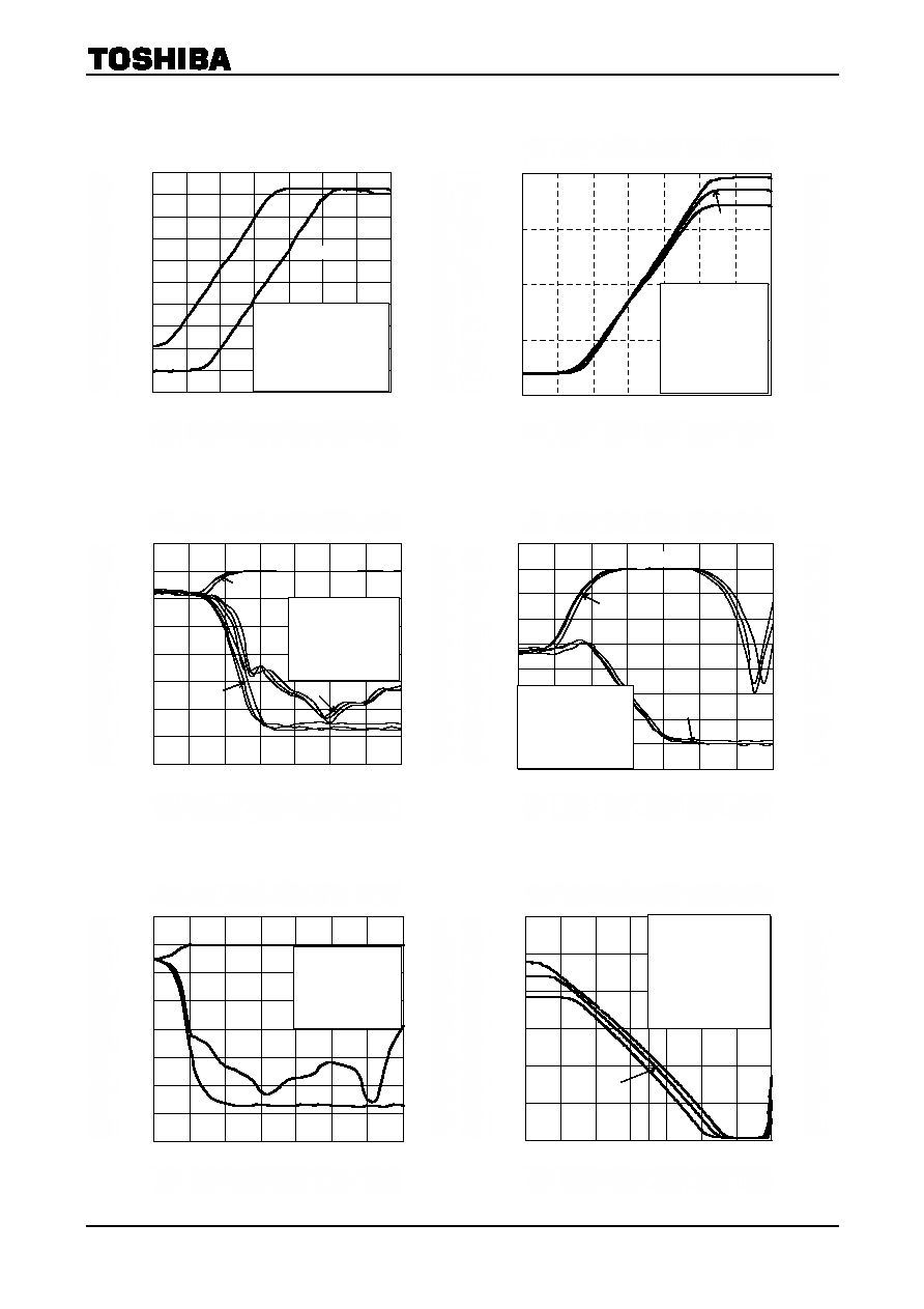
Reference Data
(This is characteristics data when it used evaluation boards. This is not
guarantee on condition that it is stating except electrical characteristics.)
S/N Characteristics (MIX input) in the
FM Mode
MIX IN input level V (MIX) in (dB
µVEMF)
S
+
N, N (dB
)
S/N Characteristics (MIX input) in the
AM Mode
MIX IN input level V (MIX) in (dB
µVEMF)
S
+
N, N (dB
)
S Curve Characteristics (MIX IN)
MIX IN input level V (MIX) in (dB
µVEMF)
S
+
N, N (dB
)
RSSI Output Voltage Characteristics
(MIX, and RF inputs)
Input level Vin (dB
µVEMF)
RSSI
output
volt
age VRSSI (V
)
RSSI Output Voltage Characteristics
(MIX inputs)
MIX IN input level V (MIX) in (dB
µVEMF)
RSSI
output
volt
age VRSSI (V
)
S/N Characteristics (RF input) in the
FM Mode
RF IN input level V (RF) in (dB
µVEMF)
S
+
N, N (dB
)
0
0.5
1
1.5
2
2.5
3
-70
-50
-30
-10
10
30
50
70
Vcc=3V
f(MIX)in=314.9MHz +f
V(MIX)in=50dBuVemf
f(Lo)in=39.38MHz
V(Lo)in=100dBuV
<Meas Point>
AFOUT
at Multi Meter
-40
125
25
0
0.5
1
1.5
2
-20
0
20
40
60
80
100
120
VCC = 3 V
f (MIX) in = 314.96 MHz
f (Lo) in = 39.38 MHz
AM
<Meas point>
FILOUT at audio analyzer
-40
25
125
0
0.2
0.4
0.6
0.8
1
1.2
1.4
1.6
1.8
2
-20
0
20
40
60
80
100
120
VCC = 3 V
f (MIX) in = 314.96 MHz
f (Lo) in = 39.38 MHz
AM
<Meas point>
FILOUT at audio analyzer
MIX IN
RF IN
-70
-60
-50
-40
-30
-20
-10
0
10
-20
0
20
40
60
80
100
120
VCC = 3 V
f (MIX) in = 314.96 MHz
Dev = 8 kHz
fmod = 600 Hz
<Meas point>
FILOUT at audio analyzer
-40
-40
-40
125
125
125
25
25
25
S
AMR
N
S+N
-80
-70
-60
-50
-40
-30
-20
-10
0
10
-20
0
20
40
60
80
100
120
VCC = 3 V
f (MIX) in = 314.96 MHz
AM = 90%
fmod = 600 Hz
<Meas point>
FILOUT at audio analyzer
125
25
-40
125
25
-40
S
N
S+N
-70
-60
-50
-40
-30
-20
-10
0
10
-20
0
20
40
60
80
100
120
VCC = 3 V
f (RF) in = 314.96 MHz
Dev = 8 kHz
fmod = 600 Hz
<Meas point>
FILOUT at audio analyzer
S
N
AMR
S+N

TA32305FN/FNG
2003-12-04
18
-20
-15
-10
-5
0
5
10
15
20
25
60
70
80
90
100
110
120
Vcc=3V
f(MIX)in=314.96MHz
V(RF)in=60dBuV
f(Lo)in=39.38MHz
U/L=OPEN
<Meas Point>
MIXOUT
at Spectrum Analyzer
0
20
40
60
80
100
120
40
50
60
70
80
90
100
110
120
Vcc=3V
<>
f(SG1,SG2)in=314.96MHz
<>
f(SG1)in=315.06MHz
f(SG2)in=315.16MHz
<Meas Point>
MIXOUT at Spectrum
Analyzer
Reference Data
(This is characteristics data when it used evaluation boards. This is not
guarantee on condition that it is stating except electrical characteristics.)
Mixer Conversion Gain Frequency
Characteristics
MIX IN input frequency f (MIX) in (MHz)
Mixer conversion gain G
V
(MIX)
(dB)
Mixer Conversion Gain ≠
Local Input Level Characteristics
Lo input level V (Lo) in (dB
µV)
Mixer conversion gain G
V
(MIX)
(dB)
Mixer Conversion Gain ≠
Supply Voltage Characteristics
Supply voltage V
CC
(V)
Mixer conversion gain G
V
(MIX)
(dB)
Mixer Intercept Point
SG input level V (MIX) in (dB
µV)
Mixer output level
V (MIX) out
(dB
µ
V)
Detuning Characteristics
Detuning frequency (kHz)
Attenuation
level (dB)
Demodulation Output ≠
Supply Voltage Characteristics (FM)
Supply voltage V
CC
(V)
Demodulation
ou
tput (mV
r
ms)
-30
-25
-20
-15
-10
-5
0
5
10
15
20
25
1
2
3
4
5
6
f(MIX)in=314.96MHz
V(MIX)in=60dBuV
f(Lo)in=39.38MHz
V(Lo)in=100dBuV
<Meas Point>
MIXOUT at
Spectrum Analyzer
-40
25
125
0
5
10
15
20
25
100
1000
Vcc=3V
V(RF)in=60dBuV
V(Lo)in=100dBuV
U/L=OPEN
<Meas Point>
MIXOUT
at Spectrum Analyzer
-40
-35
-30
-25
-20
-15
-10
-5
0
5
-60
-40
-20
0
20
40
60
Vcc=3V
f(MIX)in=314.96MHz+f
V(MIX)in=50dBuV
f(Lo)in=39.38MHz
V(Lo)in=100dBuV
Dev=±8kHz
fmod=600Hz
<Meas Point>
AFOUT at Audio Analyzer
0
20
40
60
80
100
120
140
160
1
2
3
4
5
6
f(MIX)in=314.96MHz
V(Lo)in=50dBuVemf
Dev=±8kHz
fmod=600Hz
f(Lo)in=39.38MHz
V(Lo)in=100dBuV
<Meas Point>
FILOUT
at Audio Analyzer
-40
125
25
Desired wave
Interference wave
Interference wave
Desired wave
TA32305FN/FNG
2003-12-04
19
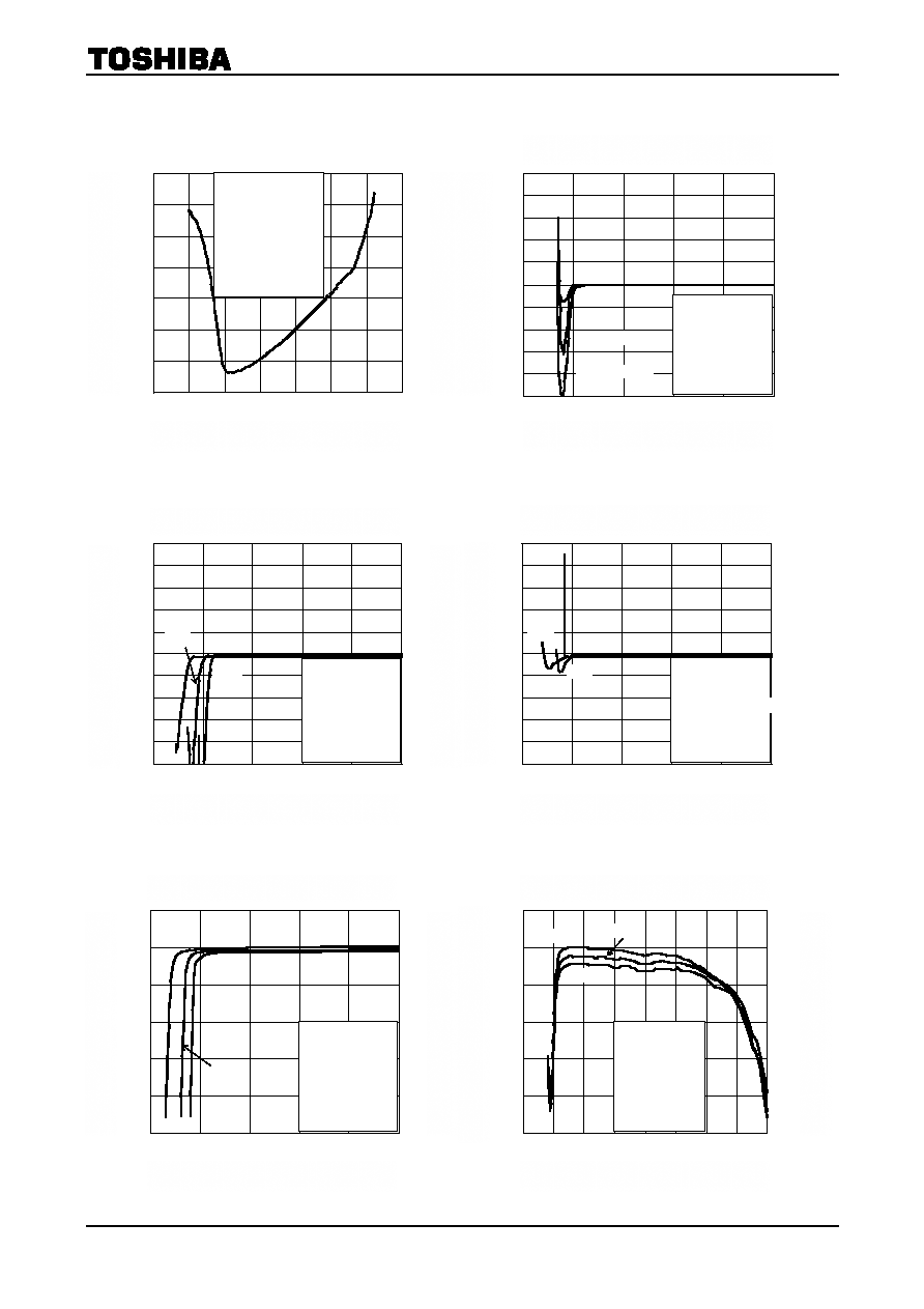
Reference Data
(This is characteristics data when it used evaluation boards. This is not
guarantee on condition that it is stating except electrical characteristics.)
Demodulation Distortion Characteristics
Detuning frequency (MIX IN) (kHz)
Demodulation
distortion (dB)
Supply voltage V
CC
(V)
W
a
ve
form shap
ing outpu
t
d
u
ty ratio
DR (%)
Waveform Shaping Output Duty Ratio ≠
Supply Voltage Characteristics FM mode
Supply voltage V
CC
(V)
W
a
ve
form shap
ing outpu
t
d
u
ty ratio
DR (%)
Waveform Shaping Output Duty Ratio ≠
Supply Voltage Characteristics
-35
-30
-25
-20
-15
-10
-5
0
-80
-60
-40
-20
0
20
40
60
Vcc=3V
f(MIX)in=314.96MHz +f
V(MIX)in=50dBuV
f(Lo)in=39.38MHz
V(Lo)in=100dBuV
<Meas Point>
AFOUT
at Audio Analyzer
40
42
44
46
48
50
52
54
56
58
60
1
2
3
4
5
6
f(MIX)in=314.96MHz
V(MIX)in=50dBuVemf
Dev=±8kHz
fmod=600Hz
f(Lo)in=39.38MHz
V(Lo)in=100dBuV
<Meas Point>
DATA at OSC
-40
125
25
40
42
44
46
48
50
52
54
56
58
60
1
2
3
4
5
6
f(MIX)in=314.96MHz
V(MIX)in=50dBuVemf
AM=90%
fmod=600Hz()
f(Lo)in=39.38MHz
V(Lo)in=100dBuV
<Meas Point>
DATA at OSC
-40
25
125
Waveform Shaping Output Duty Ratio ≠
Supply Voltage Characteristics AM mode
W
a
ve
form shap
ing outpu
t
d
u
ty ratio
DR (%)
TX Output Power ≠
Supply Voltage Characteristics
Supply voltage V
CC
(V)
T
X
O
u
tput level
V
TX1
(
d
B
)
TX Output Power Frequency Characteristics
TX output frequency f (TX)out (MHz)
T
X
O
u
tput level
V
TX1
(
d
B
)
-120
-100
-80
-60
-40
-20
0
1
2
3
4
5
6
f(Lo)in=39.38MHz
V(Lo)in=100dBuV
<Meas Point>
TX OUT at
Spectrum Analyzer
50
125
-40
25
-45
-40
-35
-30
-25
-20
-15
0
100
200
300
400
500
600
700
800
Vcc=3V
V(Lo)in=100dBuV
<Meas Point>
TX OUT at
Spectrum Analyzer
50
-40
25
125
40
42
44
46
48
50
52
54
56
58
60
1
2
3
4
5
6
f(RF)in=314.96MHz
V(RF)in=20dBuVemf
f(Lo)in=39.38MHz
V(Lo)in=100dBuV
<Meas Point>
DATA at OSC
FM Dec=±4kHz
FM Dec=±8kHz
AM
FM Dev=±8kHz
FM Dev=±4kHz
Supply voltage V
CC
(V)
(Retangle)
*Input/output
impedance
= 50
*Input/output
impedance
= 50

TA32305FN/FNG
2003-12-04
20
Reference Data
(This is characteristics data when it used evaluation boards. This is not
guarantee on condition that it is stating except electrical characteristics.)
Sensitivity Detuning Characteristics
(AM and FM modulation)
RF IN input frequency f (RF) in (MHz)
12dB SINAD sensitiv
ity
(
d
B
µ
VE
MF)
12dB SINAD sensitivity ≠
Supply Voltage Characteristics
Supply voltage V
CC
(V)
12dB SINAD sen
s
itivity
(dB
µ
VE
MF)
TX out power frequency Characteristics
TX output frequency f (TX)out (MHz)
T
X
O
u
tput level
V
TX1
(
d
B
)
RF Amp Gain + Mixer Conversion Gain ≠
Supply Voltage Characteristics
Supply voltage V
CC
(V)
RF
Amp + Mixer conversion gain
G
V
(
d
B
)
-22
-20
-18
-16
-14
-12
-10
200
250
300
350
400
450
500
Vcc=3V
V(Lo)in=100dBuV
<Meas Point>
TX OUT at
Spectrum Analyzer
25
125
-40
0
10
20
30
40
50
60
1
2
3
4
5
6
Vcc=3V
(RF)in=314.96MHz
V(RF)in=50dBuV
<Meas Point>
MIX OUTat
Spectrum Analyzer
50
-15
-10
-5
0
5
10
15
-120 -100
-80
-60
-40
-20
0
20
40
60
Vcc=3V
f(Lo)in=39.38MHz
V(Lo)in=100dBuV
U/L=OPEN
fmod=600Hz
<Meas Point>
FILOUT at
Audio Analyzer
SAW
FM Dev=±4kHz
FM Dev=±4kHz
AM
FM Dev=±8kHz
-14
-12
-10
-8
-6
-4
-2
0
2
1
2
3
4
5
6
f(RF)in=314.96MHz
f(Lo)in=39.38MHz
V(Lo)in=100dBuV
<Meas Point>
FILOUT
at Audio Analyzer
FM Dev=±4kHz
FM Dev=±4kHz
AM
FM Dev=±8kHz
2 signal interference Characteristics
(IF Filter band)
Interference wave input frequency (MHz)
Interfer
ence control ratio
(dB)
-10
0
10
20
30
40
50
60
314.6
314.7
314.8
314.9
315
315.1
315.2
315.3
f(RF)in = 314.96MHz
V(RF)in = 5.7dBuVEMF
Dev = ±8kHz
fmod = 600Hz
f(Lo)in = 39.38MHz
V(Lo)in = 100dBuV
<> 314.96MHz,
1.3dBuVEMF
*output adjusted
*No SAW filter
* Input/output impedance
= 50
<St>
TA32305FN/FNG
2003-12-04
16
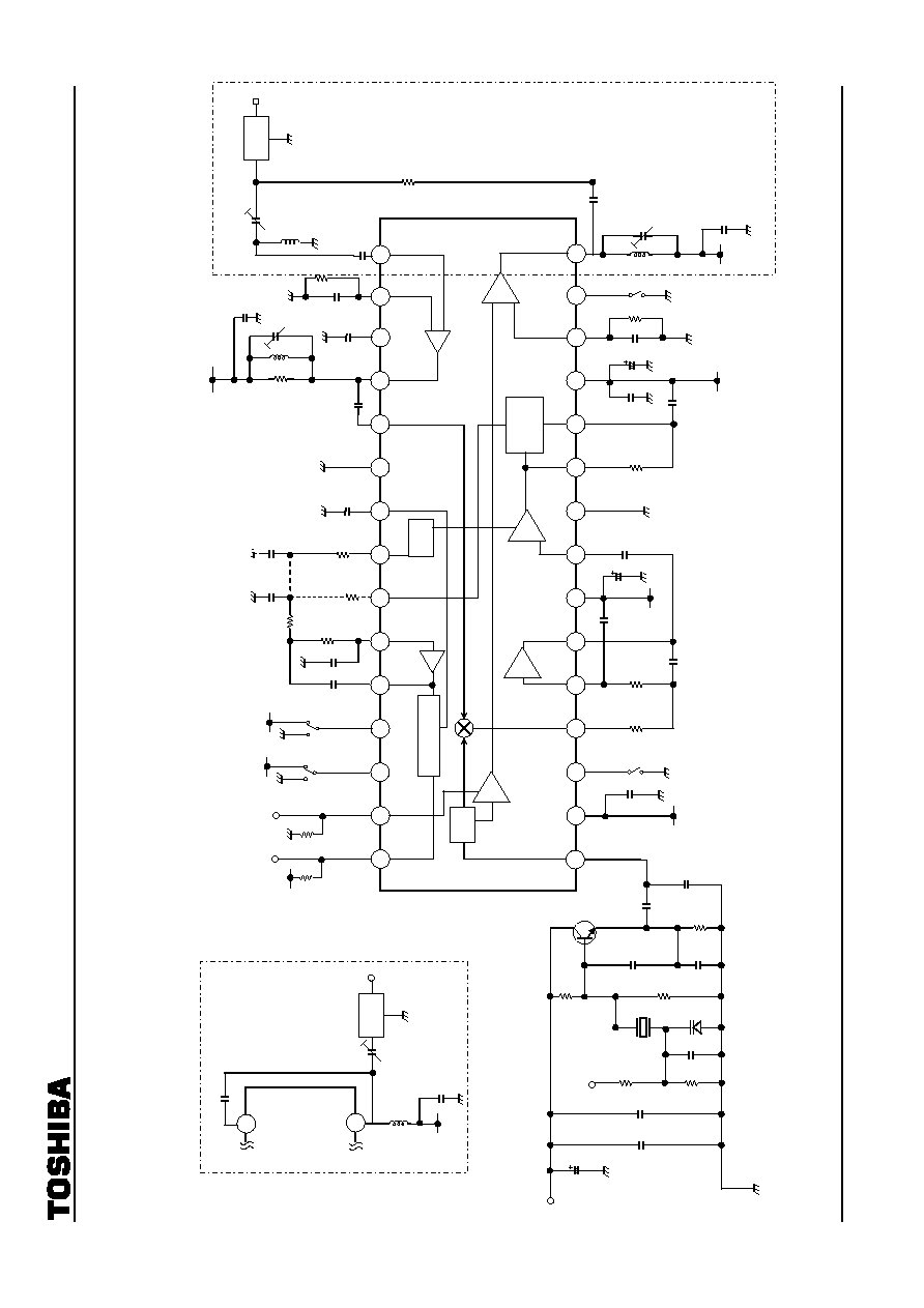
Application Circuit (ASK) *
This circuit is not guaranteed for mass product design. Please evaluate the circuit for mass product design well.
For Receiver and Transceiver
SAW: SAFCH315MAM0T00 (Murata Manufacturing)
X2: TR-1 (TEW)
Q: 2SC2499 (TOSHIBA)
12
4
3
5
6
7
8
10
11
19
27
28
26
25
24
23
22
21
20
◊8
RSSI
REF
AF
OUT
MIX
IN
GND1
RF
DEC
CHARGE
RF
IN
Vcc3
IF IN GND2
IFF
OUT
MIX
OUT
U/L
IFF
IN
OSC
IN
RF
OUT
29
30
2
1
TX LPF
OUT
LPF
IN
Detector
IF
OUT QUAD
Vcc2
V
CC
1
9
18
13
17
14
15
16
TX
Power
AM/
FM
TX
OUT
RX
TX
DATA
RX
DATA
Comparator
RSSI
SAW
1000 pF
560
R21
C35
1000 pF
C32
0.1
µ
F
C30
C22
V
CC
V
CC
V
CC
V
CC
V
CC
V
CC
V
CC
27nH
1 k
L1
R19
6 pF
0.01
µ
F
C24
C25
1000 pF
C26
C22 0.1
µ
F
68 k
R13
0.01
µ
F
560 pF
68 k
C14
C15
R12
100 k
R7
100 k
R6
0.1
µ
F
C12
R10 4.3
k
4.7 k
R11
560
R20
R22
560
C13
120 pF
10
µ
F
C17
1000
p
F
C31
L2
0.01
µ
F
1000 pF
C16
L3
33 nH
C36 5 pF
C18
3300 pF
6 pF
C37
C20 330
pF
C33
22nH
6 pF
C34
R15
43 k
Lo VCC
0.01
µ
F
5 pF
3.6 k
33 k
10
µ
F
10 pF
R3
33 pF
C1
C9
R4
33 pF
C8
C10
C7
C3
C2
R5
0.1
µ
F
X2
120 k
39.38MHz
Q
TA32305FN/FNG
2003-12-04
17
Application Circuit (FSK) *
This circuit is not guaranteed for mass product design. Please evaluate the circuit for mass product design well.
For Receiver only
SAW: SAFCH315MAM0T00 (Murata Manufacturing)
X2: TR-1 (TEW)
Q: 2SC2499 (TOSHIBA)
12
4
3
5
6
7
8
10
11
19
27
28
26
25
24
23
22
21
20
◊8
RSSI
REF
AF
OUT
MIX
IN
GND1
RF
DEC
CHARGE
RF
IN
Vcc3
IF IN GND2
IFF
OUT
MIX
OUT
U/L
IFF
IN
OSC
IN
RF
OUT
29
30
2
1
TX LPF
OUT
LPF
IN
Detector
IF
OUT QUAD
Vcc2
V
CC
1
9
18
13
17
14
15
16
TX
Power
AM/
FM
TX
OUT
RX
TX
DATA
RX
DATA
Comparator
RSSI
SAW
1000 pF
560
R21
C35
1000 pF
C32
0.1
µ
F
C30
C22
V
CC
V
CC
V
CC
V
CC
V
CC
V
CC
27nH
1 k
L1
R19
6 pF
0.01
µ
F
C24
C25
1000 pF
C26
C22 0.1
µ
F
68 k
R13
0.01
µ
F
560 pF
68 k
C14
C15
R12
100 k
R6
0.1
µ
F
C12
R10 4.3
k
4.7 k
R11
R18 20
k
C13
120 pF
10
µ
F
C17
10
µ
F
0.1
µ
F
C28
C29
C27
120 pF
1000 pF
C16
L3
33 nH
R14
68 k
C19 1000
pF
C18 3300
pF
6 pF
C37
C20 330
pF
Lo VCC
0.01
µ
F
5 pF
3.6 k
33 k
10
µ
F
10 pF
R3
33 pF
C1
C9
R4
33 pF
C8
C10
C7
C3
C2
R5
0.1
µ
F
X2
120 k
TA32305FN/FNG
2003-12-04
18
Application Circuit (FSK) *
This circuit is not guaranteed for mass product design. Please evaluate the circuit for mass product design well.
For Transceiver only:
Change the constants (X1 and R23) at oscillator circuit like the table below to be shifted oscillator frequency 10 kHz.
SAW: SAFCH315MAM0T00 (Murata Manufacturing)
X2: TR-1 (TEW)
Q: 2SC2499 (TOSHIBA)
C5: 1SV325 (TOSHIBA)
Constant
Transceiver 1
Transceiver 2
X1 39.38MHz 39.39MHz
R23 120
k 150
k
12
4
3
5
6
7
8
10
11
19
27
28
26
25
24
23
22
21
20
◊8
RSSI
REF
AF
OUT
MIX
IN
GND1
RF
DEC
CHARGE RF
IN
Vcc3
IF IN GND2
IFF
OUT
MIX
OUT
U/L
IFF
IN
OSC
IN
RF
OUT
29
30
2
TX LPF
OUT
LPF
IN
Detector
IF
OUT QUAD
Vcc2
V
CC
1
9
18
13
17
14
15
16
TX
Power
AM/
FM
TX
OUT
RX
TX
DATA
RX
DATA
Comparator
RSSI
SAW
1000 pF
560
R21
C35
1000 pF
C32
0.1
µ
F
C30
C22
V
CC
V
CC
V
CC
V
CC
V
CC
V
CC
V
CC
V
CC
27nH
1 k
L1
R19
6 pF
0.01
µ
F
C24
C25
1000 pF
C26
C22 0.1
µ
F
68 k
R13
0.01
µ
F
560 pF
68 k
C14
C15
R12
100 k
R7
100 k
R6
0.1
µ
F
C12
R10 4.3
k
4.7 k
R11
R18 20
k
560
R20
R22
560
C13
120 pF
10
µ
F
C17
10
µ
F
0.1
µ
F
1000
p
F
C28
C29
C31
C27
120 pF
L2
5 pF
1000 pF
C16
L3
33 nH
C36 5
pF
R14
68 k
C19 1000
pF
C18 3300
pF
6 pF
C37
C20 330
pF
C33
22nH
6 pF
C34
Lo VCC
0.01
µ
F
5 pF
3.6 k
33 k
10
µ
F
10 pF
R3
47 pF
C1
C9
R4
47 pF
C8
C10
C7
C3
C2
R5
0.1
µ
F
X1
1
TX FM
R23
R1
120 k
200 k
C5
C4
5
p
F
Q
TA32305FN/FNG
2003-12-04
19
Application Circuit *
This circuit is not guaranteed for mass product design. Please evaluate the circuit for mass product design well.
For Transceiver, one antenna version:
Adjust the circuit expect antenna block. In case of Hi power output application, set the circuit like left figure.
12
4
3
5
6
7
8
10
11
19
27
28
26
25
24
23
22
21
20
◊8
RSSI
REF
AF
OUT
MIX
IN
GND1
RF
DEC
CHARGE RF
IN
Vcc3
IF IN GND2
IFF
OUT
MIX
OUT
U/L
IFF
IN
OSC
IN
RF
OUT
29
30
2
TX LPF
OUT
LPF
IN
Detector
IF
OUT QUAD
Vcc2
V
CC
1
9
18
13
17
14
15
16
TX
Power
AM/
FM
TX
OUT
RX
TX
DATA
RX
DATA
Comparator
RSSI
SAW
1000 pF
560
R21
C35
1000 pF
C32
0.1
µ
F
C30
C22
V
CC
V
CC
V
CC
V
CC
V
CC
V
CC
V
CC
V
CC
27nH
1 k
L1
R19
6 pF
0.01
µ
F
C24
C25
1000 pF
C26
C22 0.1
µ
F
68 k
R13
0.01
µ
F
560 pF
68 k
C14
C15
R12
100 k
R7
100 k
R6
0.1
µ
F
C12
R10 4.3
k
4.7 k
R11
R18 20
k
560
R20
C13
120 pF
10
µ
F
C17
10
µ
F
0.1
µ
F
1000
p
F
C28
C29
C31
C27
120 pF
L2
0.01
µ
F
1000 pF
C16
L3
33 nH
C36
5 pF
R14
68 k
C19 1000
pF
C18 3300
pF
6 pF
C37
C20 330
pF
C33
22nH
6 pF
C34
Lo VCC
0.01
µ
F
5 pF
3.6 k
33 k
10
µ
F
10 pF
R3
47 pF
C1
C9
R4
47 pF
C8
C10
C7
C3
C2
R5
0.1
µ
F
X1
1
TX FM
R23
R1
120 k
120 k
200 k
C5
C4
5
p
F
39.38MHz
Q
R24
300
R15
43 k
RF
IN
15
16
TX
OUT
C35
V
CC
L2
0.01
µ
F
C33
22nH
SAW
6 pF
Hi Power Output

TA32305FN/FNG
2003-12-04
20
Package Dimensions
SSOP30-P-300-0.65A Unit::mm
Weight: 0.17 g (typ)

TA32305FN/FNG
2003-12-04
21
∑ TOSHIBA is continually working to improve the quality and reliability of its products. Nevertheless, semiconductor
devices in general can malfunction or fail due to their inherent electrical sensitivity and vulnerability to physical
stress. It is the responsibility of the buyer, when utilizing TOSHIBA products, to comply with the standards of
safety in making a safe design for the entire system, and to avoid situations in which a malfunction or failure of
such TOSHIBA products could cause loss of human life, bodily injury or damage to property.
In developing your designs, please ensure that TOSHIBA products are used within specified operating ranges as
set forth in the most recent TOSHIBA products specifications. Also, please keep in mind the precautions and
conditions set forth in the "Handling Guide for Semiconductor Devices," or "TOSHIBA Semiconductor Reliability
Handbook" etc..
∑ The TOSHIBA products listed in this document are intended for usage in general electronics applications
(computer, personal equipment, office equipment, measuring equipment, industrial robotics, domestic appliances,
etc.). These TOSHIBA products are neither intended nor warranted for usage in equipment that requires
extraordinarily high quality and/or reliability or a malfunction or failure of which may cause loss of human life or
bodily injury ("Unintended Usage"). Unintended Usage include atomic energy control instruments, airplane or
spaceship instruments, transportation instruments, traffic signal instruments, combustion control instruments,
medical instruments, all types of safety devices, etc.. Unintended Usage of TOSHIBA products listed in this
document shall be made at the customer's own risk.
∑ The products described in this document are subject to the foreign exchange and foreign trade laws.
∑ The information contained herein is presented only as a guide for the applications of our products. No
responsibility is assumed by TOSHIBA CORPORATION for any infringements of intellectual property or other
rights of the third parties which may result from its use. No license is granted by implication or otherwise under
any intellectual property or other rights of TOSHIBA CORPORATION or others.
∑ The information contained herein is subject to change without notice.
000707EBA
RESTRICTIONS ON PRODUCT USE
Notice for Pb free product
About solderability, following conditions were confirmed
Solderability
(1) Use of Sn-36Pb solder bath
solder bath temperature = 230
dipping time = 5seconds
the number of times = once
use of R-type flux
(2) Use of Sn-3.0Ag-0.5Cu solder bath
solder bath temperature = 245
dipping time = 5seconds
the number of times = once
use of R-type flux