TA4012AFE
2002-01-18
1
TOSHIBA Bipolar Linear Integrated Circuit Silicon Monolithic
TA4012AFE
UHF Wide Band Amplifier Applications
Features
∑ Low current: I
CC
= 6.5 mA
∑ Wide band: f = 2.0 GHz (3dB down)
∑ Operating supply voltage: V
CC
= 1.5~2.2 V
Maximum Ratings
(Ta
=
=
=
=
25∞C)
Characteristics Symbol
Rating
Unit
Supply voltage 1
V
CC
1
2.2 V
Supply voltage 2
(Note1)
V
CC
2 3 V
Total power dissipation
(Note2)
P
D
300
mW
Operating temperature
T
opr
-
40~85 ∞C
Storage temperature
T
stg
-
55~150 ∞C
Note1: When
V
CC
is operated at less than 1/4 duty cycle
Note2: When mounted on the glass epoxy of 2.5 cm
2
¥
1.6 t
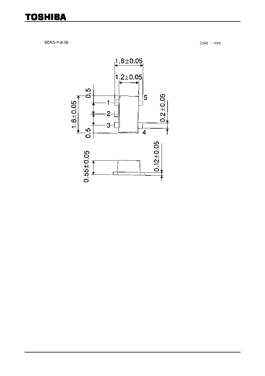
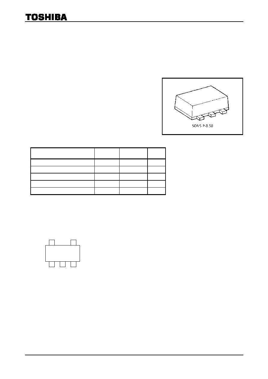
Marking
Weight: 0.003 g (typ.)
OUT
U 4
COLLECTOR
V
CC
GND IN
5 4
1 2 3

TA4012AFE
2002-01-18
2
Electrical Characteristics
(Ta
=
=
=
=
25∞C, Zg
=
=
=
=
Zl
=
=
=
=
50
W
W
W
W
)
Characteristics Symbol
Test
Condition
Min
Typ.
Max
Unit
Circuit current
I
CC
V
CC
=
2 V, non carrier
4.5
6.5
8.5
mA
Band width
BW
V
CC
=
2 V
(Note3)
1.8
2.0
æ
GHz
Insertion gain
Ô
S21
Ô
2
V
CC
=
2 V, f
=
1.5 GHz
10
12
æ
dB
Noise figure
NF
V
CC
=
2 V, f
=
1.5 GHz
æ
6 7.5 dB
Isolation
Ô
S12
Ô
2
V
CC
=
2 V, f
=
1.5 GHz
æ
-
22
æ
dB
Input return loss
Ô
S11
Ô
2
V
CC
=
2 V, f
=
1.5 GHz
æ
-
6.5
æ
dB
Output return loss
Ô
S22
Ô
2
V
CC
=
2 V, f
=
1.5 GHz
æ
-
7.5
æ
dB
Output power at 1 dB gain compression
Po1dB
V
CC
=
2 V, f
=
1.5 GHz
æ
0
æ
dBmW
Note3: BW is the frequency of 3dB down from
Ô
S21
Ô
2
at 1.5 GHz.
Caution
This device is sensitive to electrostatic discharge. When using this device, please ensure that all tools and
equipment are earthed.
RF Test Circuit
(top view)
Notice
The circuits and measurements contained in this document are given only in the context of as examples of
applications for these products.
Moreover, these example application circuits are not intended for mass production, since the high-frequency
characteristics (the AC characteristics) of these devices will be affected by the external components which the
customer uses, by the design of the circuit and by various other conditions.
It is the responsibility of the customer to design external circuits which correctly implement the intended
application, and to check the characteristics of the design.
TOSHIBA assume no responsibility for the integrity of customer circuit designs or applications.
Equivalent Circuit
3
4
2
5
1
RF IN
GND
100 pF
1000 pF
10000 pF
L
RF OUT
1000 pF
1000 pF
L: 4 nh
2
1
3
5
4
V
CC
TA4012AFE
2002-01-18
4
∑
TOSHIBA is continually working to improve the quality and reliability of its products. Nevertheless, semiconductor
devices in general can malfunction or fail due to their inherent electrical sensitivity and vulnerability to physical
stress. It is the responsibility of the buyer, when utilizing TOSHIBA products, to comply with the standards of
safety in making a safe design for the entire system, and to avoid situations in which a malfunction or failure of
such TOSHIBA products could cause loss of human life, bodily injury or damage to property.
In developing your designs, please ensure that TOSHIBA products are used within specified operating ranges as
set forth in the most recent TOSHIBA products specifications. Also, please keep in mind the precautions and
conditions set forth in the "Handling Guide for Semiconductor Devices," or "TOSHIBA Semiconductor Reliability
Handbook" etc..
∑
The TOSHIBA products listed in this document are intended for usage in general electronics applications
(computer, personal equipment, office equipment, measuring equipment, industrial robotics, domestic appliances,
etc.). These TOSHIBA products are neither intended nor warranted for usage in equipment that requires
extraordinarily high quality and/or reliability or a malfunction or failure of which may cause loss of human life or
bodily injury ("Unintended Usage"). Unintended Usage include atomic energy control instruments, airplane or
spaceship instruments, transportation instruments, traffic signal instruments, combustion control instruments,
medical instruments, all types of safety devices, etc.. Unintended Usage of TOSHIBA products listed in this
document shall be made at the customer's own risk.
∑
The products described in this document are subject to the foreign exchange and foreign trade laws.
∑
The information contained herein is presented only as a guide for the applications of our products. No
responsibility is assumed by TOSHIBA CORPORATION for any infringements of intellectual property or other
rights of the third parties which may result from its use. No license is granted by implication or otherwise under
any intellectual property or other rights of TOSHIBA CORPORATION or others.
∑
The information contained herein is subject to change without notice.
000707EBA
RESTRICTIONS ON PRODUCT USE