 | –≠–ª–µ–∫—Ç—Ä–æ–Ω–Ω—ã–π –∫–æ–º–ø–æ–Ω–µ–Ω—Ç: TA48018S | –°–∫–∞—á–∞—Ç—å:  PDF PDF  ZIP ZIP |

TA48018,02,025,03,033,05F/S
2004-07-01
1
TOSHIBA Bipolar Linear Integrated Circuit Silicon Monolithic
TA48018F,
TA4802F, TA48025F, TA4803F, TA48033F,
TA4805F,
TA48018S, TA4802S, TA48025S, TA4803S, TA48033S, TA4805S
1.8 V, 2 V, 2.5 V, 3 V, 3.3 V, 5 V
Three-Terminal Low Dropout Voltage Regulator with Output Current of 1 A
The TA48**F/S series consists of fixed-positive-output,
low-dropout regulators with an output current of 1 A (max) that
utilize V-PNP transistors for the output stage. In response to the
need for low-voltage and low-power dissipation devices which are
used in consumer electronics and industrial appliances, the series
offers devices with low output voltages: 1.8 V, 2 V, 2.5 V, 3 V, 3.3
V, 5 V.
Features
Maximum output current: 1 A
Output voltage accuracy: V
OUT
± 3% (@T
j
= 25∞C)
Low standby current: 800 µA (typ.) (@I
OUT
= 0 A)
Low starting quiescent current
Low-dropout voltage: V
D
= 0.5 V (max) (@I
OUT
= 0.5 A)
Protection function: overheat/overcurrent
Package type: PW-MOLD (TA48**F Series)
TO-220NIS (TA48**S Series)
TA48**F Series has a lead bending type package which is a
surface-mountable package and can be used for reflow
soldering.
Pin Assignment
Marking
(1) (2) TA48F** Series
(3) TA48**S Series
Note: The "**" part of each product number varies according to the output voltage of the product.
(1) TA48**F
(2) TA48**F (TE16L1, N)
(3) TA48**S
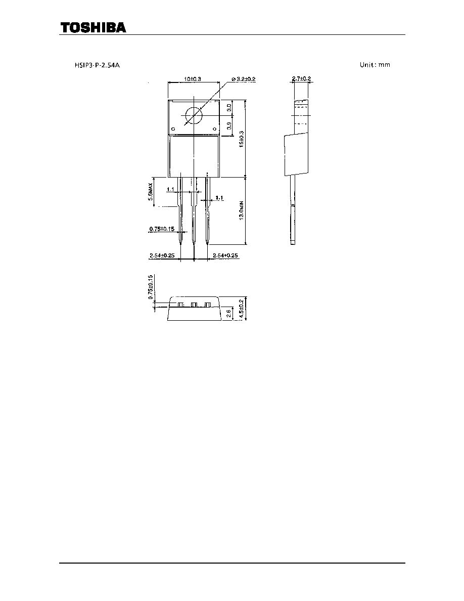
Weight
HSIP3-P-2.30B : 0.36 g (typ.)
HSOP3-P-2.30D : 0.36 g (typ.)
HSIP3-P-2.54A : 1.7 g (typ.)
TA48**S
Lot No.
(weekly code)
A line indicates
lead (Pb)-free package or
lead (Pb)-free finish.
Part No. (or abbreviation code)
48**F
Lot No.
(weekly code)
A line indicates
lead (Pb)-free package or
lead (Pb)-free finish.
Part No. (or abbreviation code)
1
OUT
Marking side
3
2
GND
IN

TA48018,02,025,03,033,05F/S
2004-07-01
2
How to Order
Product No.
Package
Packing Type and Unit for Orders
(1) TA48**F
PW-MOLD: Straight-lead package
Loose in bag: 200 (1 bag)
(2) TA48**F (TE16L1, N)
PW-MOLD: Surface-mount package Embossed-tape packing: 2000 (1 tape)
(3) TA48**S
TO-220NIS
Loose in bag: 50 (1 bag)
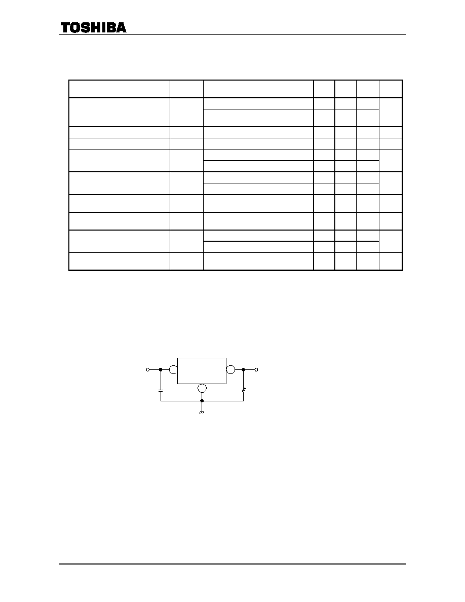
Block Diagram
Maximum Ratings
(Ta = 25∞C)
Characteristic Symbol
Rating
Unit
Input voltage
V
IN
16 V
Output current
I
OUT
1 A
Operating temperature
Ta
(opr)
-40~85 ∞C
Junction temperature
T
j
150 ∞C
Storage temperature
T
stg
-55~150 ∞C
TA48**F 1
Power dissipation
(Ta = 25∞C)
TA48**S
P
D
2
W
TA48**F 10
Power dissipation
(Tc = 25∞C)
TA48**S
P
D
20
W
TA48**F 125
Thermal resistance
(junction to ambient)
TA48**S
R
th (j-a)
62.5
∞C/W
TA48**F 12.5
Thermal resistance
(junction to case)
TA48**S
R
th (j-c)
6.25
∞C/W
Note 1: External current and voltage ((including negative voltage) should not be applied to pins not specified.
1
IN
Overcurrent-
limiting circuit
2
OUT
3
GND
Overheating
detection circuit
Reference
voltage circuit
Constant
current circuit

TA48018,02,025,03,033,05F/S
2004-07-01
3
Protection Function (reference)
Characteristics Symbol
Test
Condition
Min
Typ.
Max
Unit
Thermal shutdown
T
SD
(T
j
)
160 ∞C
V
IN
= V
OUT
+ 2 V, T
j
= 25∞C
1.7
Peak circuit current
I
PEAK
V
IN
= 12 V, T
j
= 25∞C
1.8
A
V
IN
= V
OUT
+ 2 V, T
j
= 25∞C
1.7
Short circuit current
I
SC
V
IN
= 12 V, T
j
= 25∞C
1.8
A
Note 2: The maximum ratings should not be exceeded when the IC is actually used.
TA48018F/S
Electrical Characteristics
(Unless otherwise specified C
IN
= 0.33
µ
F, C
OUT
= 10
µ
F, T
j
= 25∞C)
Characteristics Symbol Test
Conditions Min
Typ.
Max
Unit
V
IN
= 3.8 V, I
OUT
= 0.5 A
1.746
1.8
1.854
Output voltage
V
OUT
2.8 V <= V
IN
<
= 12 V, 5 mA <= I
OUT
<
= 1 A,
0∞C <= T
j
<
= 125∞C
1.72 1.8 1.88
V
Line regulation
Regline
2.8 V <= V
IN
<
= 12 V, I
OUT
= 0.5 A
5 20 mV
Load regulation
Regload
V
IN
= 3.8 V, 5 mA <= I
OUT
<
= 1 A
5 20 mV
2.8 V <= V
IN
<
= 12 V, I
OUT
= 0 A
0.8 1.8
Quiescent current
I
B
2.8 V <= V
IN
<
= 12 V, I
OUT
= 1 A
10 20
mA
V
IN
= 2.1 V, I
OUT
= 0 A
0.7 5
Starting quiescent current
I
Bstart
V
IN
= 2.5 V, I
OUT
= 1 A
10 30
mA
Output noise voltage
V
NO
V
IN
= 3.8 V, I
OUT
= 50 mA
10 Hz <= f <= 100 kHz
75
µVrms
Ripple rejection
R.R.
2.8 V <= V
IN
12 V, I
OUT
= 50 mA
f = 120 Hz
54 70 dB
I
OUT
= 0.5 A
0.3 0.5
Dropout voltage
V
D
I
OUT
= 1 A
0.7
V
Average temperature coefficient of
output voltage
T
CVO
V
IN
= 3.8 V, I
OUT
= 5 mA,
0∞C <= T
j
<
= 125∞C
0.15 mV/∞C

TA48018,02,025,03,033,05F/S
2004-07-01
4
TA4802F/S
Electrical Characteristics
(Unless otherwise specified, C
IN
= 0.33
µ
F, C
OUT
= 10
µ
F, T
j
= 25∞C)
Characteristics Symbol Test
Conditions Min
Typ.
Max
Unit
V
IN
= 4.0 V, I
OUT
= 0.5 A
1.94
2.0
2.06
Output voltage
V
OUT
3.0 V <= V
IN
<
= 12 V, 5 mA <= I
OUT
<
= 1 A,
0∞C <= T
j
<
= 125∞C
1.91 2.0 2.09
V
Line regulation
Regline
3.0 V <= V
IN
<
= 12 V, I
OUT
= 0.5 A
5 20 mV
Load regulation
Regload
V
IN
= 4.0 V, 5 mA <= I
OUT
<
= 1 A
5 20 mV
3.0 V <= V
IN
<
= 12 V, I
OUT
= 0 A
0.8 1.8
Quiescent current
I
B
3.0 V <= V
IN
<
= 12 V, I
OUT
= 1 A
10 20
mA
V
IN
= 2.1 V, I
OUT
= 0 A
0.7 5
Starting quiescent current
I
Bstart
V
IN
= 2.6 V, I
OUT
= 1 A
10 30
mA
Output noise voltage
V
NO
V
IN
= 4.0 V, I
OUT
= 50 mA
10 Hz <= f <= 100 kHz
80
µVrms
Ripple rejection
R.R.
3.0 V <= V
IN
12 V, I
OUT
= 50 mA
f = 120 Hz
52 68 dB
I
OUT
= 0.5 A
0.3 0.5
Dropout voltage
V
D
I
OUT
= 1 A
0.6
V
Average temperature coefficient of
output voltage
T
CVO
V
IN
= 4.0 V, I
OUT
= 5 mA,
0∞C <= T
j
<
= 125∞C
0.18 mV/∞C
TA48025F/S
Electrical Characteristics
(Unless otherwise specified, C
IN
= 0.33
µ
F, C
OUT
= 10
µ
F, T
j
= 25∞C)
Characteristics Symbol Test
Conditions Min
Typ.
Max
Unit
V
IN
= 4.5 V, I
OUT
= 0.5 A
2.425
2.5
2.575
Output voltage
V
OUT
3.5 V <= V
IN
<
= 12 V, 5 mA <= I
OUT
<
= 1 A,
0∞C <= T
j
<
= 125∞C
2.388 2.5 2.612
V
Line regulation
Regline
3.5 V <= V
IN
<
= 12 V, I
OUT
= 0.5 A
5 20 mV
Load regulation
Regload
V
IN
= 4.5 V, 5 mA <= I
OUT
<
= 1 A
5 20 mV
3.5 V <= V
IN
<
= 12 V, I
OUT
= 0 A
0.8 1.8
Quiescent current
I
B
3.5 V <= V
IN
<
= 12 V, I
OUT
= 1 A
10 20
mA
V
IN
= 2.1 V, I
OUT
= 0 A
0.9 5
Starting quiescent current
I
Bstart
V
IN
= 2.65 V, I
OUT
= 1 A
12 30
mA
Output noise voltage
V
NO
V
IN
= 4.5 V, I
OUT
= 50 mA
10 Hz <= f <= 100 kHz
95
µVrms
Ripple rejection
R.R.
3.5 V <= V
IN
12 V, I
OUT
= 50 mA
f = 120 Hz
52 68 dB
I
OUT
= 0.5 A
0.3 0.5
Dropout voltage
V
D
I
OUT
= 1 A
0.4
V
Average temperature coefficient of
output voltage
T
CVO
V
IN
= 4.5 V, I
OUT
= 5 mA,
0∞C <= T
j
<
= 125∞C
0.24 mV/∞C

TA48018,02,025,03,033,05F/S
2004-07-01
5
TA4803F/S
Electrical Characteristics
(Unless otherwise specified, C
IN
= 0.33
µ
F, C
OUT
= 10
µ
F, T
j
= 25∞C)
Characteristics Symbol Test
Conditions Min
Typ.
Max
Unit
V
IN
= 5.0 V, I
OUT
= 0.5 A
2.91
3.0
3.09
Output voltage
V
OUT
4.0 V <= V
IN
<
= 12 V, 5 mA <= I
OUT
<
= 1 A,
0∞C <= T
j
<
= 125∞C
2.865 3.0 3.135
V
Line regulation
Regline
4.0 V <= V
IN
<
= 12 V, I
OUT
= 0.5 A
5 20 mV
Load regulation
Regload
V
IN
= 5.0 V, 5 mA <= I
OUT
<
= 1 A
5 20 mV
4.0 V <= V
IN
<
= 12 V, I
OUT
= 0 A
0.8 1.8
Quiescent current
I
B
4.0 V <= V
IN
<
= 12 V, I
OUT
= 1 A
10 20
mA
V
IN
= 2.1 V, I
OUT
= 0 A
1.1 5
Starting quiescent current
I
Bstart
V
IN
= 2.8 V, I
OUT
= 1 A
13 30
mA
Output noise voltage
V
NO
V
IN
= 5.0 V, I
OUT
= 50 mA
10 Hz <= f <= 100 kHz
110
µVrms
Ripple rejection
R.R.
4.0 V <= V
IN
12 V, I
OUT
= 50 mA
f = 120 Hz
50 66 dB
I
OUT
= 0.5 A
0.3 0.5
Dropout voltage
V
D
I
OUT
= 1 A
0.4
V
Average temperature coefficient of
output voltage
T
CVO
V
IN
= 5.0 V, I
OUT
= 5 mA,
0∞C <= T
j
<
= 125∞C
0.28 mV/∞C
TA48033F/S
Electrical Characteristics
(Unless otherwise specified, C
IN
= 0.33
µ
F, C
OUT
= 10
µ
F, T
j
= 25∞C)
Characteristics Symbol Test
Conditions Min
Typ.
Max
Unit
V
IN
= 5.3 V, I
OUT
= 0.5 A
3.2
3.3
3.4
Output voltage
V
OUT
4.3 V <= V
IN
<
= 12 V, 5 mA <= I
OUT
<
= 1 A,
0∞C <= T
j
<
= 125∞C
3.152 3.3 3.448
V
Line regulation
Regline
4.3 V <= V
IN
<
= 12 V, I
OUT
= 0.5 A
5 20 mV
Load regulation
Regload
V
IN
= 5.3 V, 5 mA <= I
OUT
<
= 1 A
5 20 mV
4.3 V <= V
IN
<
= 12 V, I
OUT
= 0 A
0.8 1.8
Quiescent current
I
B
4.3 V <= V
IN
<
= 12 V, I
OUT
= 1 A
10 20
mA
V
IN
= 2.1 V, I
OUT
= 0 A
1.1 5
Starting quiescent current
I
Bstart
V
IN
= 2.8 V, I
OUT
= 1 A
13 30
mA
Output noise voltage
V
NO
V
IN
= 5.3 V, I
OUT
= 50 mA
10 Hz <= f <= 100 kHz
115
µVrms
Ripple rejection
R.R.
4.3 V <= V
IN
12 V, I
OUT
= 50 mA
f = 120 Hz
50 66 dB
I
OUT
= 0.5 A
0.3 0.5
Dropout voltage
V
D
I
OUT
= 1 A
0.4
V
Average temperature coefficient of
output voltage
T
CVO
V
IN
= 5.3 V, I
OUT
= 5 mA,
0∞C <= T
j
<
= 125∞C
0.3 mV/∞C
TA48018,02,025,03,033,05F/S
2004-07-01
6
TA4805F/S
Electrical Characteristics
(Unless otherwise specified, C
IN
= 0.33
µ
F, C
OUT
= 10
µ
F, T
j
= 25∞C)
Characteristics Symbol Test
Conditions Min
Typ.
Max
Unit
V
IN
= 7 V, I
OUT
= 0.5 A
4.85
5.0
5.15
Output voltage
V
OUT
6.0 V <= V
IN
<
= 12 V, 5 mA <= I
OUT
<
= 1 A,
0∞C <= T
j
<
= 125∞C
4.775 5.0 5.225
V
Line regulation
Regline
6.0 V <= V
IN
<
= 12 V, I
OUT
= 0.5 A
5 20 mV
Load regulation
Regload
V
IN
= 7.0 V, 5 mA <= I
OUT
<
= 1 A
5 20 mV
6.0 V <= V
IN
<
= 12 V, I
OUT
= 0 A
0.8 1.8
Quiescent current
I
B
6.0 V <= V
IN
<
= 12 V, I
OUT
= 1 A
10 20
mA
V
IN
= 2.1 V, I
OUT
= 0 A
1.3 5
Starting quiescent current
I
Bstart
V
IN
= 3.0 V, I
OUT
= 1 A
14 30
mA
Output noise voltage
V
NO
V
IN
= 7.0 V, I
OUT
= 50 mA
10 Hz <= f <= 100 kHz
150
µVrms
Ripple rejection
R.R.
6.0 V <= V
IN
12 V, I
OUT
= 50 mA
f = 120 Hz
50 64 dB
I
OUT
= 0.5 A
0.3 0.5
Dropout voltage
V
D
I
OUT
= 1 A
0.4
V
Average temperature coefficient of
output voltage
T
CVO
V
IN
= 7.0 V, I
OUT
= 5 mA,
0∞C <= T
j
<
= 125∞C
0.45 mV/∞C
Electrical Characteristics for All Products
Generally, the characteristics of power supply ICs change according to temperature fluctuations.
The specification T
j
= 25 is based on a state where temperature increase has no effect (assuming no fluctuation
in the characteristics) as ascertained by pulse tests.
Standard Application Circuit
Be sure to connect a capacitor near the input terminal and output terminal between both terminals and GND.
The capacitances should be determined experimentally. In particular, adequate investigation should be made so
that there is no problem even in high or low temperature.
1
2
V
IN
TA48xxF/S
3
V
OUT
C
OUT
C
IN
0.33
µF 33
µF

TA48018,02,025,03,033,05F/S
2004-07-01
7
TA48**F
P
Dmax
≠ Ta
TA48**S
P
Dmax
≠ Ta
V
OUT
≠ T
j
V
OUT
≠ V
IN
I
B
≠ V
IN
I
B
≠ T
j
Ambient temperature Ta (∞C)
Ambient temperature Ta (∞C)
Junction temperature Tj (∞C)
Input voltage VIN (V)
Input voltage VIN (V)
Junction temperature Tj (∞C)
Allo
w
abl
e p
o
w
e
r
dis
s
i
patio
n
P
Dm
a
x
(W
)
Allo
w
abl
e
p
o
we
r
dis
s
ip
atio
n P
Dmax
(W
)
Outp
ut v
o
ltag
e
V
OUT
(V
)
Outp
ut v
o
ltag
e
V
OUT
(V
)
Qu
i
e
sce
nt
c
u
r
r
e
n
t
I
B
(m
A
)
Qu
i
e
sce
nt
c
u
r
r
e
n
t
I
B
(m
A
)
0
12
2
160
0 100
60
8
6
10
20 80 140
Ta
= Tc
4
40 120
30
◊ 30 ◊ 0.8 mmt
Single
50
◊ 50 ◊ 0.8 mmt
Condition:
Number of IC = 1
Reflow soldering on
a ceramic substrate
0
24
4
160
0 100
60
16
12
20
20
80
140
Ta
= Tc
8
40
120
No heat sink
Thermal resistance
Rth (j-a): 62.5∞C/W
Rth (j-c): 6.25∞C/W
3.1
3.5
150
-50
3.3
3.4
50
3.2
0 100
TA48033F/S
VIN = 5 V
IOUT = 5 mA
IOUT = 1 A
0
20
8
16
4
150
-50
50
0 100
TA48033F/S
VIN = 5 V
12
IOUT = 0 A
IOUT = 0.5 A
0
10
4
8
2
8
0 4
2 6
TA48033F/S
Tj = 25∞C
6
IOUT = 0.1 A
IOUT = 10 mA
0
4
8
0
2
3
4
1
2 6
TA48033F/S
Tj = 25∞C
0.5 A
0.1 A
IOUT = 10 mA

TA48018,02,025,03,033,05F/S
2004-07-01
8
I
B
≠ I
OUT
V
OUT
≠ I
OUT
V
D
≠ T
j
R.R. ≠ f
Output current IOUT (A)
Output current IOUT (A)
Junction temperature Tj (∞C)
Frequency f (kHz)
Outp
ut v
o
ltag
e
V
OUT
(V
)
Qu
i
e
sce
nt
c
u
r
r
e
n
t
I
B
(m
A
)
Ri
pple
rej
e
c
t
i
on
R
.
R
.
(d
B
)
D
r
op
out
vol
t
a
ge
V
D
(V
)
0
20
8
16
4
1
0 0.4
0.2 0.8
12
TA48033F/S
VIN = 5 V
Tj = 25∞C
0.6
0
70
30
60
10
100
0.1
1
40
10
20
50
TA48033F/S
VIN = 5 V
IOUT = 50 mA
Tj = 25∞C
2
0 1
0.5
1.5
TA48033F/S
VIN = 5 V
Tj = 25∞C
0
1
2
4
3
IOUT = 0.1 A
0
0.6
0.2
0.5
0.1
150
-50 50
0
0.4
TA48033F/S
100
IOUT = 0.5 A
IOUT = 1 A
0.3

TA48018,02,025,03,033,05F/S
2004-07-01
9
Package Dimensions
Weight: 0.36 g (typ.)

TA48018,02,025,03,033,05F/S
2004-07-01
10
Package Dimensions
Weight: 0.36 g (typ.)
TA48018,02,025,03,033,05F/S
2004-07-01
11
Package Dimensions
Weight: 1.7 g (typ.)

TA48018,02,025,03,033,05F/S
2004-07-01
12
∑ The information contained herein is subject to change without notice.
∑ The information contained herein is presented only as a guide for the applications of our products. No
responsibility is assumed by TOSHIBA for any infringements of patents or other rights of the third parties which
may result from its use. No license is granted by implication or otherwise under any patent or patent rights of
TOSHIBA or others.
∑ TOSHIBA is continually working to improve the quality and reliability of its products. Nevertheless, semiconductor
devices in general can malfunction or fail due to their inherent electrical sensitivity and vulnerability to physical
stress. It is the responsibility of the buyer, when utilizing TOSHIBA products, to comply with the standards of
safety in making a safe design for the entire system, and to avoid situations in which a malfunction or failure of
such TOSHIBA products could cause loss of human life, bodily injury or damage to property.
In developing your designs, please ensure that TOSHIBA products are used within specified operating ranges as
set forth in the most recent TOSHIBA products specifications. Also, please keep in mind the precautions and
conditions set forth in the "Handling Guide for Semiconductor Devices," or "TOSHIBA Semiconductor Reliability
Handbook" etc..
∑ The TOSHIBA products listed in this document are intended for usage in general electronics applications
(computer, personal equipment, office equipment, measuring equipment, industrial robotics, domestic appliances,
etc.). These TOSHIBA products are neither intended nor warranted for usage in equipment that requires
extraordinarily high quality and/or reliability or a malfunction or failure of which may cause loss of human life or
bodily injury ("Unintended Usage"). Unintended Usage include atomic energy control instruments, airplane or
spaceship instruments, transportation instruments, traffic signal instruments, combustion control instruments,
medical instruments, all types of safety devices, etc.. Unintended Usage of TOSHIBA products listed in this
document shall be made at the customer's own risk.
∑ The products described in this document are subject to the foreign exchange and foreign trade laws.
∑ TOSHIBA products should not be embedded to the downstream products which are prohibited to be produced
and sold, under any law and regulations.
030619EBA
RESTRICTIONS ON PRODUCT USE