 | –≠–ª–µ–∫—Ç—Ä–æ–Ω–Ω—ã–π –∫–æ–º–ø–æ–Ω–µ–Ω—Ç: TA6042FNG | –°–∫–∞—á–∞—Ç—å:  PDF PDF  ZIP ZIP |

TA6042FNG
TA6042FNG Data Sheet Revision 0.9 2005-07-22
1
TOSHIBA Bipolar Linear Integrated Circuit Silicon Monolithic
TA6042FNG
Shock sensor IC for signal processing
TA6042FNG performs the signal processing in response to the
amplification signal of a shock sensor.
Features
∑ TA6042FNG is operated under 4.5 ~ 5.5 V DC single power
supply voltage.
∑ User can make notch-filter circuit with OP-AMP2 and
external element, and adjust gain by changing R1/R2 Ratio.
∑ To change the g-force sensing level, user can adjust gain by
changing R7/R8 ratio.
∑ The Window comparator has a hysteresis which width is
about 150mV.
∑ Small package: SSOP10-P-0.65A (0.65 mm pitch)
Block Diagram
Weight: 0.04 g (Type.)
Preliminary
GND
VCC
+
-
-
+
4
7
OP-AMP3
OP-AMP2
5
-
+
1
8
6
9
3
10
2
R0
R0
R6
R5
R3
R4
C1
C2
C3
CP
AMP
-
+
AMP
-
+
Vref
2V
OP-AMP1
DET
COUT
NOUT
NIN
DOUT
DIN2
DIN1
CIN
CMP2
-
+
CMP1
-
+
3V
1V
R1
R2
R1
R2
R7
R7
R8
C4

TA6042FNG
TA6042FNG Data Sheet Revision 0.9 2005-07-22
2
Pin Function
Pin No.
Pin Name
Function
1 CIN
OP-AMP3
input terminal
(Shock sensor amplification signal input)
2 COUT
OP-AMP3
output terminal
3 DET
Window Comparator
output terminal
("L" is outputted at the time of shock detection.)
4 GND
Ground
terminal
5 NOUT
OP-AMP2
output terminal
6 NIN
OP-AMP2
input terminal
7 V
CC
Power
supply
voltage
8 DOUT
OP-AMP1
output terminal
9 DIN2
OP-AMP1 - side
input terminal
(Shock sensor amplification signal input)
10 DIN1
OP-AMP1 + side
input terminal
(Shock sensor amplification signal input)
Pin Connection
(top view)
DIN1
10
DIN2
DOUT
V
CC
NIN
9
8
7
6
CIN
1
2
3
4
5
COUT
DET
GND
NOUT

TA6042FNG
TA6042FNG Data Sheet Revision 0.9 2005-07-22
3
Maximum Ratings
(Ta
= 25∞C)
Characteristics Symbol
Rating
Unit
Power supply voltage
V
CC
7 V
Power dissipation
P
D
300
mW
Storage temperature
T
stg
-55~150 ∞C
Recommend Operating Condition
Characteristics Symbol
Rating
Unit
Power supply voltage
V
CC
4.5~5.5 V
Operating temperature
T
opr
-25~85 ∞C
Note: The IC may be destroyed due to short circuit between adjacent pins, incorrect orientation of device's mounting,
connecting positive and negative power supply pins wrong way round, air contamination fault, or fault by
improper grounding.
Please consider the voltage-drop caused by OP-AMP3 input current and feedback resistance (R8), and
examine the value of the feedback resistance.
We will recommend 500k or less as a value of the feedback resistance.
TA6042FNG is Pd free product..
The following conditions apply to solderability:
*Solderability
1. Use of Sn-63Pb solder bath
*solder bath temperature=230 degrees
*dipping time=5seconds
*number of times=once
*use of R-type flux
2. Use of Sn-3.0Ag-0.5Cu solder bath
*solder bath temperature=245 degrees
*dipping time=5seconds
*the number of times=once
*use of R-type flux

TA6042FNG
TA6042FNG Data Sheet Revision 0.9 2005-07-22
4
Electrical Characteristics
(unless otherwise specified, V
CC
= 5.0 V, Ta = 25∞C)
Characteristics Symbol
Test
Circuit
Test Condition
Min
Typ.
Max
Unit
Supply voltage
V
CC
4.5 5.0 5.5 V
Supply current
I
CC
(1) Max:Vcc=5.5V
2.5 mA
(OP-AMP1)
Characteristics Symbol
Test
Circuit
Test Condition
Min
Typ.
Max
Unit
Input current
Iin1
(2)
35 80 nA
Output dynamic range
Vod1
(3)
0.3
Vcc-0.3
V
Output source current
Iso1
(4) Voh
= V
CC
- 0.3 V
100
250
µA
Output sink current
Isi1
(5) Vol
= 0.3 V
2
11
mA
(OP-AMP2)
Characteristics Symbol
Test
Circuit
Test Condition
Min
Typ.
Max
Unit
Input current
Iin2
(6)
35 80 nA
Output dynamic range
Vod2
(7)
0.3
Vcc-0.3
V
Output source current
Iso2
(8) Voh
= V
CC
- 0.3 V
100
190
µA
Output sink current
Isi2
(9) Vol
= 0.3 V
2
11
mA
Output DC voltage
Vo2
5pin - 6pin: Short Circuit,
8pin - 9pin: Short Circuit,
8pin output voltage:2.0V setup.
(The voltage input from 10pin)
0.98 1.00 1.02 V
(OP-AMP3)
Characteristics Symbol
Test
Circuit
Test Condition
Min
Typ.
Max
Unit
Input current
Iin3
(10)
35 80 nA
Output dynamic range
Vod3
(11)
0.3
Vcc-0.3
V
Output source current
Iso3
(12)
Voh
= V
CC
- 0.3 V
100
180
µA
Output sink current
Isi3
(13)
Vol
= 0.3 V
2
11
mA
Output DC voltage
Vo3
(14)
1.86
2.00
2.14
V
(Window Comparator)
Characteristics Symbol
Test
Circuit
Test Condition
Min
Typ.
Max
Unit
Hysteresis width
Vwhys
(15)
100 150 200
mV
Detection voltage level (High side)
Vwsh
(16)
2.79 3.00 3.21
V
Detection voltage level (Low side)
Vwsl
(16)
0.93 1.00 1.07
V
Output sink current
Iwsi
(17)
Vol
= 0.3 V
0.30
1.39
mA

TA6042FNG
TA6042FNG Data Sheet Revision 0.9 2005-07-22
5
Electrical Characteristics (2) --- Reference data for application (Note)
(OP-AMP1)
Characteristics Symbol
Test
Circuit
Test Condition
Min
Typ.
Max
Unit
GBW (Cutoff frequency)
fT1
2.0
3.0
MHz
Openloop gain
Gvo1
80
90
dB
Offset voltage
Voff1
-5 0 5 mV
(OP-AMP2)
Characteristics Symbol
Test
Circuit
Test Condition
Min
Typ.
Max
Unit
GBW (Cutoff frequency)
fT2
2.0
3.0
MHz
Openloop gain
Gvo2
85
95
dB
(OP-AMP3)
Characteristics Symbol
Test
Circuit
Test Condition
Min
Typ.
Max
Unit
GBW (Cutoff frequency)
fT3
1.5
2.0
MHz
Openloop gain
Gvo3
85
95
dB

TA6042FNG
TA6042FNG Data Sheet Revision 0.9 2005-07-22
6
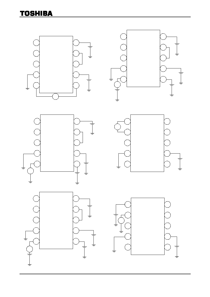
TEST Circuit
Supply current
Input current=A1/2
1
2
3
4
5
10
9
8
7
6
Vcc
OP-AMP1
Input current
1
2
3
4
5
10
9
8
7
6
Output dynamic range
(Low side)(High side)
Vcc
V
1
2
3
4
5
10
9
8
7
6
A
Vcc
OP-AMP1
Output source current
OP-AMP1
Output sink current
1.0V
Vcc-0.3V
1
2
3
4
5
10
9
8
7
6
A
Vcc
0.3V
3.5V
2.5V
2.5V
2.5V
2.5V
1.0V & 3.0V
A1
A
Vcc
1
2
3
4
5
10
9
8
7
6
510
15p
510
360
16
1
750
7.5
75k
2.5V
100
18
TA6042FNG
TA6042FNG Data Sheet Revision 0.9 2005-07-22
7
OP-AMP2
Output source current
1
2
3
4
5
10
9
8
7
6
A
Vcc
Vcc-0.3V
1.0V
2.5V
1
2
3
4
5
10
9
8
7
6
OP-AMP2
Output dynamic range
(Low side)(High side)
Vcc
V
2.5V
1.0V & 3.0V
OP-AMP2
Output sink current
1
2
3
4
5
10
9
8
7
6
Vcc
3.5V
2.5V
A
0.3V
1
2
3
4
5
10
9
8
7
6
Vcc
OP-AMP3
Input current
A
1
2
3
4
5
10
9
8
7
6
OP-AMP3
Output dynamic range
(Low side)(High side)
Vcc
V
1.0V & 3.0V
1
2
3
4
5
10
9
8
7
6
Vcc
OP-AMP
Input current
2.5V
A

TA6042FNG
TA6042FNG Data Sheet Revision 0.9 2005-07-22
8
OP-AMP3
Output sink current
1
2
3
4
5
10
9
8
7
6
Vcc
OP-AMP3
Output DC voltage
1
2
3
4
5
10
9
8
7
6
Vcc
A
0.3V
3.5V
V
Window-Comparator
Hysteresis width
Window-Comparator
Detection voltage level
(High side)(Low side)
Window-Comparator
Output sink current
1
2
3
4
5
10
9
8
7
6
Vcc
OP-AMP3
Output source current
A
Vcc-0.3V
1.0V
1
2
3
4
5
10
9
8
7
6
Vcc
M2
10k
1.8k
M1
1F
8.2k
1
2
3
4
5
10
9
8
7
6
Vcc
0.3V
A
1.5V
10k
100k
1
2
3
4
5
10
9
8
7
6
Vcc
M2
10k
1.8k
M1
1F
8.2k
1000pF
1000pF

TA6042FNG
TA6042FNG Data Sheet Revision 0.9 2005-07-22
9
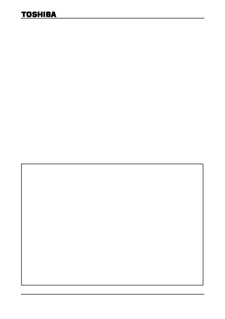
Package Dimensions
Weight: 0.04 g (typ.)
TA6042FNG
TA6042FNG Data Sheet Revision 0.9 2005-07-22
10
∑ The information contained herein is subject to change without notice.
∑ The information contained herein is presented only as a guide for the applications of our products. No
responsibility is assumed by TOSHIBA for any infringements of patents or other rights of the third parties which
may result from its use. No license is granted by implication or otherwise under any patent or patent rights of
TOSHIBA or others.
∑ TOSHIBA is continually working to improve the quality and reliability of its products. Nevertheless, semiconductor
devices in general can malfunction or fail due to their inherent electrical sensitivity and vulnerability to physical
stress. It is the responsibility of the buyer, when utilizing TOSHIBA products, to comply with the standards of
safety in making a safe design for the entire system, and to avoid situations in which a malfunction or failure of
such TOSHIBA products could cause loss of human life, bodily injury or damage to property.
In developing your designs, please ensure that TOSHIBA products are used within specified operating ranges as
set forth in the most recent TOSHIBA products specifications. Also, please keep in mind the precautions and
conditions set forth in the "Handling Guide for Semiconductor Devices," or "TOSHIBA Semiconductor Reliability
Handbook" etc..
∑ The TOSHIBA products listed in this document are intended for usage in general electronics applications
(computer, personal equipment, office equipment, measuring equipment, industrial robotics, domestic appliances,
etc.). These TOSHIBA products are neither intended nor warranted for usage in equipment that requires
extraordinarily high quality and/or reliability or a malfunction or failure of which may cause loss of human life or
bodily injury ("Unintended Usage"). Unintended Usage include atomic energy control instruments, airplane or
spaceship instruments, transportation instruments, traffic signal instruments, combustion control instruments,
medical instruments, all types of safety devices, etc.. Unintended Usage of TOSHIBA products listed in this
document shall be made at the customer's own risk.
∑ TOSHIBA products should not be embedded to the downstream products which are prohibited to be produced
and sold, under any law and regulations.
030619EAA
RESTRICTIONS ON PRODUCT USE