 | –≠–ª–µ–∫—Ç—Ä–æ–Ω–Ω—ã–π –∫–æ–º–ø–æ–Ω–µ–Ω—Ç: TA7291AS | –°–∫–∞—á–∞—Ç—å:  PDF PDF  ZIP ZIP |
TA7291AP/AS(J)/AF
2003-02-14
1
TOSHIBA Bipolar Linear Integrated Circuit Silicon Monolithic
TA7291AP,TA7291AS(J),TA7291AF
Full-Bridge Driver for DC Motors (driver for controlling the forward and reverse rotations)
The TA7291AP/TA7291AS (J)/TA7291AF is a full-bridge driver to
control the forward and reverse rotations. Each driver can select
one of four modes: CW, CCW, stop, brake.
The TA7291AP is designed to provide output currents of 1.0 A (typ.)
and 2.0 A (peak). The TA7291AS (J)/TA7291AF is designed to
provide output currents of 0.4 A (typ.) and 1.2 A (peak).
There are two different power supply pins for each driver: one on
the output side and the other on the control side of the driver. Also,
there is the V
ref
pin on the output side. This pin is available for
adjusting the voltage supplied to the motor.
The input circuit of the driver is compatible with CMOS logic
because it draws a small amount of input current.
Features
∑ Wide range of operating voltage: V
CC (opr.)
= 4.5 V to 27 V
:
V
S (opr.)
= 4.5 V to 27 V
:
V
ref (opr.)
= 4.5 V to 27 V
V
ref
must be V
S
.
∑ Output current: AP type 1.0 A (typ.) 2.0 A (peak)
: AS (J)/AF type 0.4 A (typ.) 1.2 A (peak)
∑ Thermal shutdown and overcurrent protection
∑ Flyback diodes
∑ Hysteresis for all inputs
∑ Standby mode available
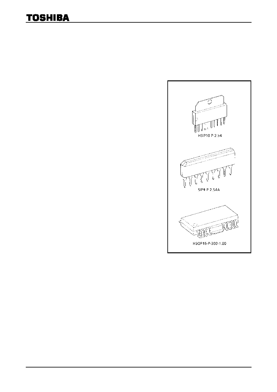
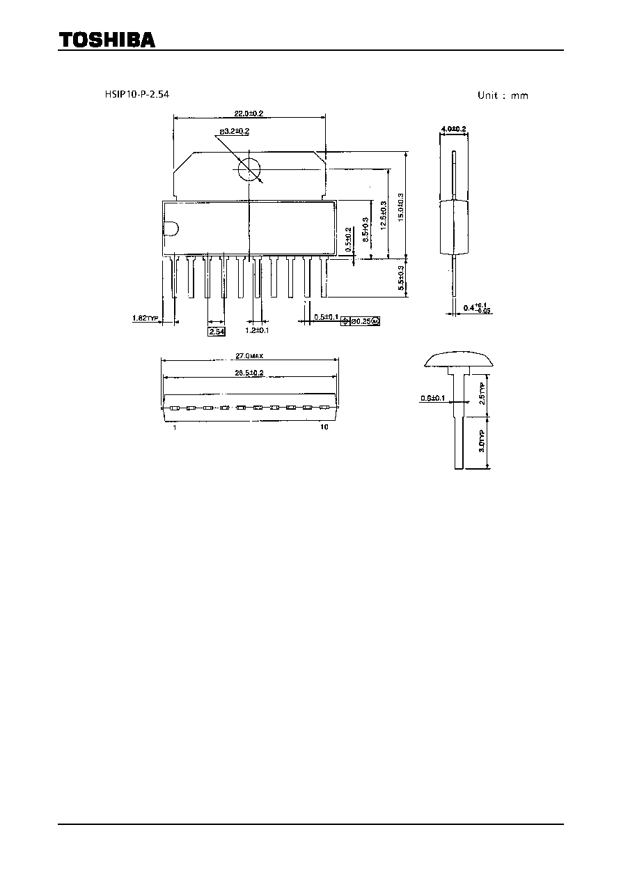
TA7291AP
TA7291AS (J)
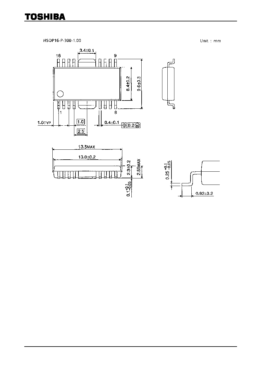
TA7291AF
Weight
HSIP10-P-2.54: 2.47 g (typ.)
SIP9-P-2.54A: 0.92 g (typ.)
HSOP16-P-300-1.00: 0.50 g (typ.)
TA7291AP/AS(J)/AF
2003-02-14
2
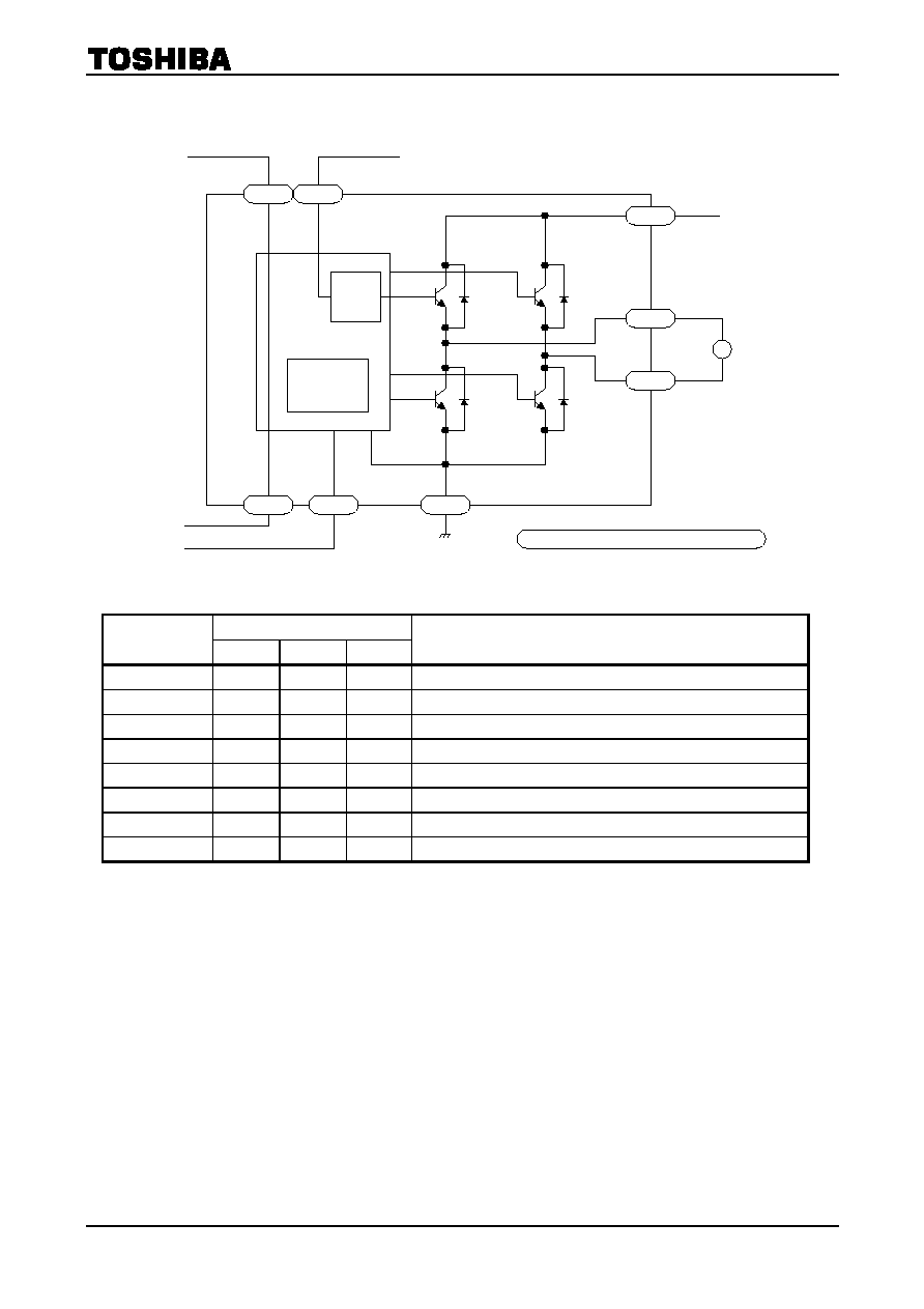
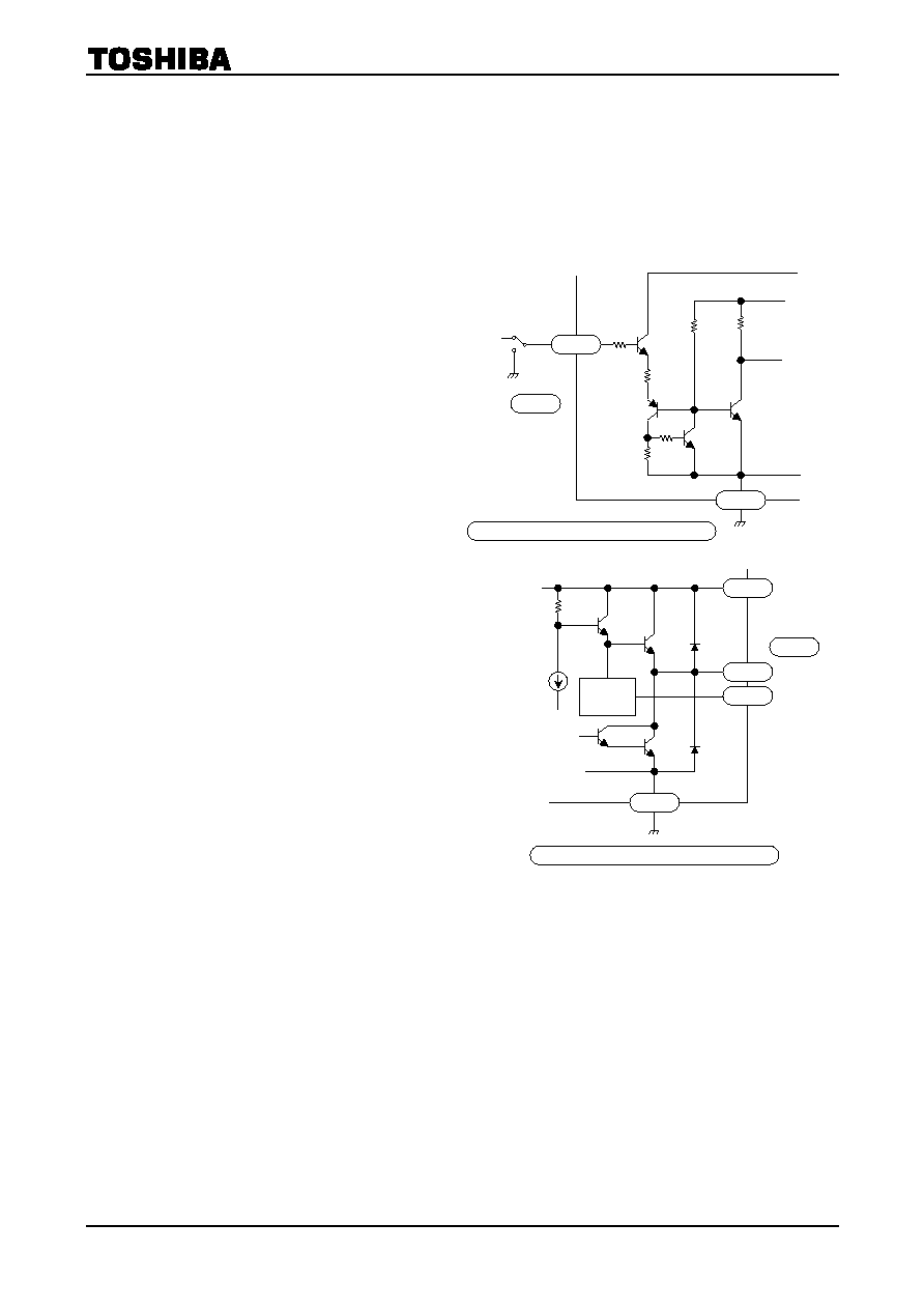
Block Diagram
Pin Function
Pin No.
Symbol
AP AS
(J) AF
Function Description
V
CC
7
2
11
Supply voltage pin for Logic
V
S
8
6
15
Supply voltage pin for motor driver
V
ref
4
8
5
Supply voltage pin for control
GND 1
5
1
Ground
pin
IN1 5
9
7
Input
pin
IN2 6
1
9
Input
pin
OUT1 2
7
4
Output
pin
OUT2 10
3
13
Output
pin
AP type: Pin 3 and 9 are NC.
AS (J) type: Pin 4 is NC.
AF type: Pin 2, 3, 6, 8, 10, 12, 14, and 16 are NC.
For F type, we recommend the fin be connected to ground.
Protection
circuit
(TSD)
7/2/11
4/8/5
5/9/7
6/1/9
REG
M
2/7/4
10/3/13
8/6/15
1/5/1
V
CC
V
ref
IN1
IN2
GND
V
S
OUT1
OUT2
TA7291AP/TA7291AS (J)/TA7291AF

TA7291AP/AS(J)/AF
2003-02-14
3
Function
Input Output
IN1 IN2 OUT1
OUT2
Mode
0 0
Stop
1 0 H L
CW/CCW
0 1 L H
CCW/CW
1 1 L L
Brake
: High
impedance
Note: Inputs are all active high.
Maximum Ratings
(Ta = 25∞C)
Characteristics Symbol
Rating Unit
V
CC
30
Supply voltage
V
CC (opr.)
27
V
V
S
30
Motor drive voltage
V
S (opr.)
27
V
V
ref
30
Reference voltage
V
ref (opr.)
27
V
AP type
2.0
Peak
AS (J)/AF type
I
O (peak)
1.2
P type
1.0
Output
current
Typ.
S(J)/AF type
I
O (typ.)
0.4
A
AP type
12.5 (Note 1)
AS (J) type
0.95 (Note 2)
Power dissipation
AF type
P
D
1.4
(Note
3)
W
Operating temperature
T
opr
-30 to 75
∞C
Storage temperature
T
stg
-55 to 150
∞C
Note 1: Tc
= 25∞C
Note 2: No heat sink
Note 3: When mounted on a PCB (PCB area: 60 mm
¥ 30 mm ¥ 1.6 mm, Cu area: 50% or more)
Wide range of operating voltage: V
CC (opr.)
= 4.5 V to 27 V
V
S (opr.)
= 4.5 V to 27 V
V
ref (opr.)
= 4.5 V to 27 V
V
ref
V
S
TA7291AP/AS(J)/AF
2003-02-14
4
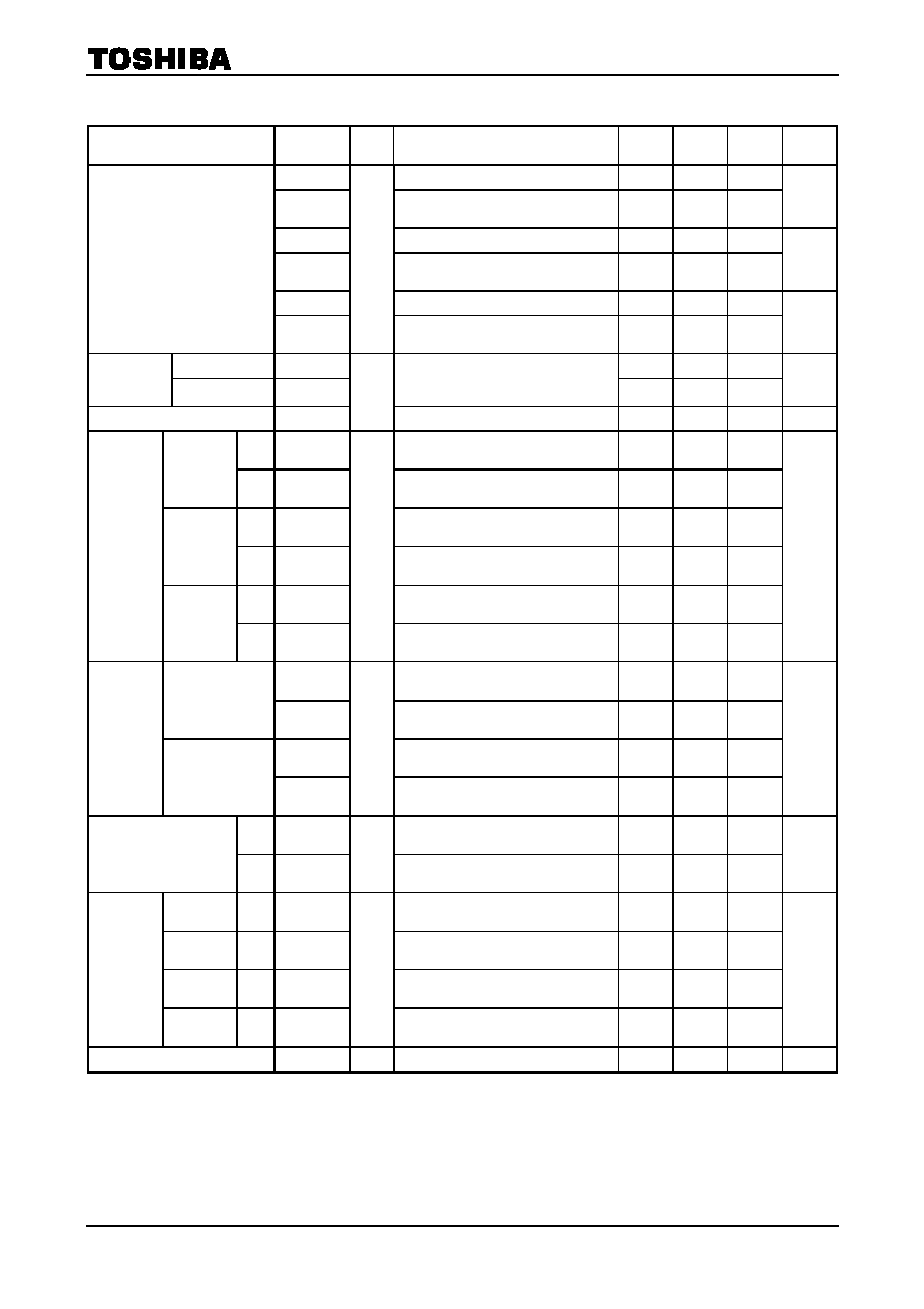
Electrical Characteristics
(Ta
=
=
=
=
25∞C, V
CC
=
=
=
=
5 V, V
S
=
=
=
=
24 V)
Characteristics Symbol
Test
Circuit
Test Condition
Min
Typ.
Max
Unit
I
CC1-1
Output OFF, CW/CCW mode
æ
6.0 11.0
I
CC1-2
Output OFF, CW/CCW mode,
V
CC
= 24 V
æ 8.0 13.0
mA
I
CC2-1
Output OFF, Stop mode
æ 0 50
I
CC2-2
Output OFF, Stop mode,
V
CC
= 24 V
æ 0 50
mA
I
CC3-1
Output OFF, Brake mode
æ 4.5 8.0
Supply current
I
CC3-2
1
Output OFF, Brake mode,
V
CC
= 24 V
æ 6.5 10.0
mA
1 (High)
V
IN1
3.5
æ 5.5
Input
operating
voltage
2 (Low)
V
IN2
T
j
= 25∞C
GND
æ 0.8
V
Input current
I
IN
2
V
IN
= 3.5 V, Sink mode
æ 3 10 mA
Upper
side
V
SAT U-1
V
ref
= V
S
, V
OUT
-V
S
measure
I
O
= 0.2 A, CW/CCW mode
æ 0.9 1.2
AP/AS (J)/
AF type
Lower
side
V
SAT L-1
V
ref
= V
S
, V
OUT
-GND measure
I
O
= 0.2 A, CW/CCW mode
æ 0.8 1.2
Upper
side
V
SAT U-2
V
ref
= V
S
, V
OUT
-V
S
measure
I
O
= 0.4 A, CW/CCW mode
æ 1.0 1.35
AS (J)/AF
type
Lower
side
V
SAT L-2
V
ref
= V
S
, V
OUT
-GND measure
I
O
= 0.4 A, CW/CCW mode
æ 0.9 1.35
Upper
side
V
SAT U-3
V
ref
= V
S
, V
OUT
-V
S
measure
I
O
= 1.0 A, CW/CCW mode
æ 1.3 1.8
Saturation
voltage
AP type
Lower
side
V
SAT L-3
3
V
ref
= V
S
, V
OUT
-GND measure
I
O
= 1.0 A, CW / CCW mode
æ 1.2 1.85
V
V
SAT U-1'
V
ref
: 10 V, V
OUT
-GND measure
I
O
= 0.2 A, CW / CCW mode
æ 11.2 æ
AS (J)/AF type
V
SAT U-2'
V
ref
: 10 V, V
OUT
-GND measure
I
O
= 0.4 A, CW/CCW mode
10.4 10.9 12.2
V
SAT U-3'
V
ref
: 10 V, V
OUT
-GND measure
I
O
= 0.5 A, CW/CCW mode
æ 11.0 æ
Output
voltage
(upper
side)
AP type
V
SAT U-4'
3
V
ref
: 10 V, V
OUT
-GND measure
I
O
= 1.0 A, CW/CCW mode
10.2 10.7 12.0
V
Upper
side
I
L U
V
L
= 30 V
æ
æ 50
Leakage current
Lower
side
I
L L
4
V
L
= 30 V
æ
æ 50
mA
AS (J)/AF
type
Upper
side
V
F U-1
æ
æ 1.5 æ
AP type
Lower
side
V
F U-2
æ
æ 2.5 æ
AS (J)/AF
type
Upper
side
V
F L-1
æ
æ 0.9 æ
Diode
forward
voltage
AP type
Lower
side
V
F L-2
5
æ
æ 1.2 æ
V
Reference current
I
ref
2 V
ref
= 10 V, Source mode
æ
æ 40 mA

TA7291AP/AS(J)/AF
2003-02-14
5
Test Circuit 1
I
CC1-1
, I
CC1-2
, I
CC2-1
,I
CC2-2
, I
CC3-1
, I
CC3-2
Note: The heat fin of the TA7291AF is connected to ground.
Test Circuit 2
V
IN1
, V
IN2
, I
IN
, I
ref
Note: The heat fin of the TA7291AF is connected to ground.
OUT1
7/2/11
1/5/1
4/8/5
10/3/13
8/6/15
2/7/4
GND
V
IN2
TA7291AP/AS (J)/AF
5/9/7
6/1/9
A
V
IN
V
S
V
S
=
24
V
V
re
f
10 V
V
IN1
SW
1
SW
2
OUT2
A
5 V (max)
0 V (min)
SW
3
V
CC
5 V
TA7291AP/TA7291AS (J)/TA7291AF
7/2/11
1/5/1
4/8/5
10/3/13
8/6/15
2/7/4
GND
V
IN2
TA7291AP/AS (J)/AF
5/9/7
6/1/9
A
V
IN (H)
V
CC
5 V
/
24
V
V
S
V
S
=
24
V
3.
5 V
V
IN1
SW
1
SW
2
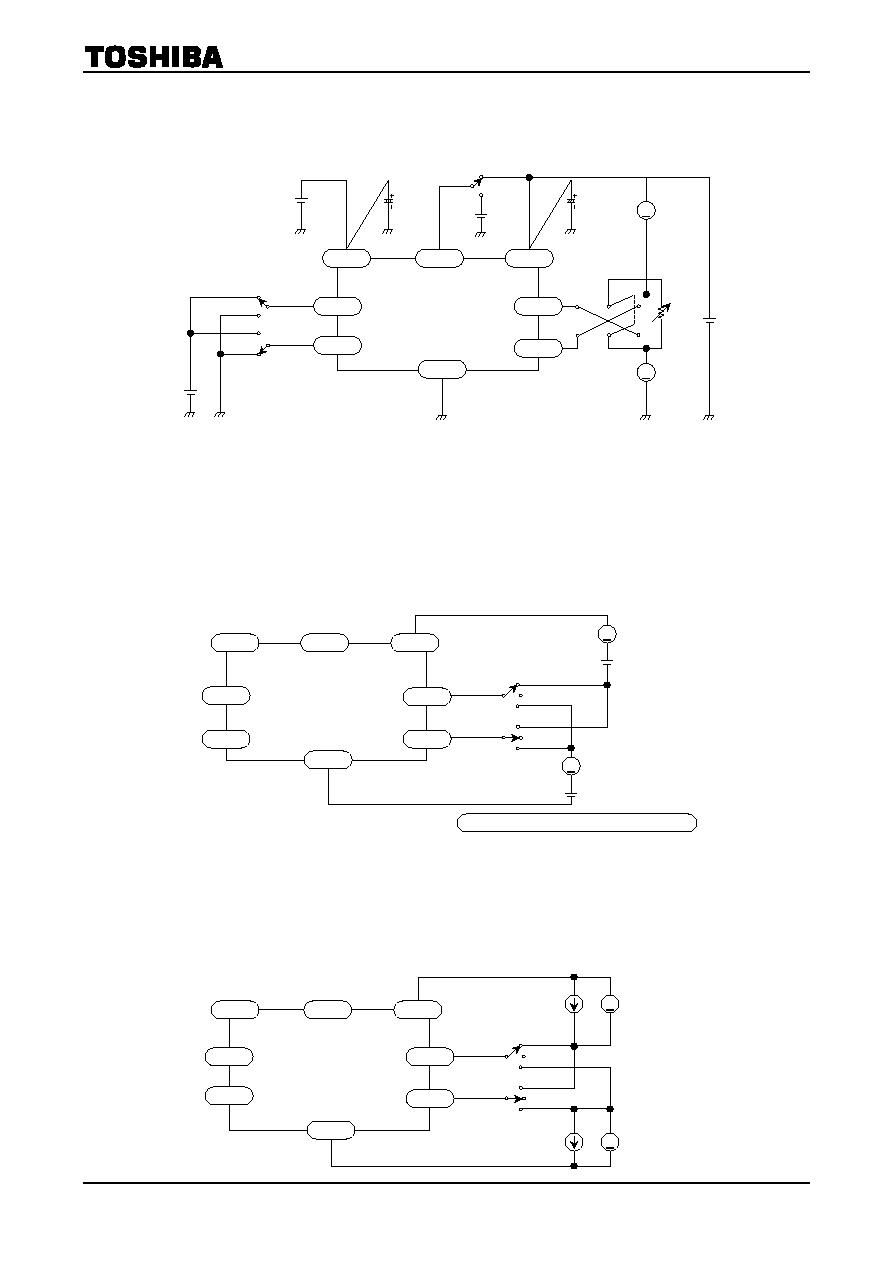
TA7291AP/AS(J)/AF
2003-02-14
6
Test Circuit 3.
V
SAT
U-1
,
2
,
3
V
SAT
L-1
,
2
,
3
V
SAT
U-1'
,
2'
,
3'
,
4'
Note 1: I
OUT
calibration is required to adjust specified values of test conditions by R
L
.
(I
OUT
= 0.2 A/0.4 A/0.5 A/1.0 A)
Note 2: The heat fin of the TA7291AF is connected to ground.
Test Circuit 4.
I
LU
, L
Note: The heat fin of the TA7291AF is connected to ground.
Test Circuit 5.
V
F U-1
,
2
V
F L-1
,
2
SW
2
SW
1
OUT1
4/8/5
10/3/13
2/7/4
TA7291AP/AS (J)/AF
5/9/7
6/1/9
OUT2
7/2/11
I
L
V
S
V
V
U
V
U
1/5/1
V
I
U
8/6/15
OUT1
7/2/11
1/5/1
4/8/5
10/3/13
8/6/15
2/7/4
GND
V
IN2
TA7291AP/AS (J)/AF
5/9/7
6/1/9
V
IN
(H)
V
S
V
S
=
24
V
V
IN1
SW
2
OUT2
V
CC
3.
5 V
SW
1
5 V
10 V
SW
4
V
ref
V
S
V
V
SW
3
R
L
(
)
OUT1
4/8/5
10/3/13
2/7/4
TA7291AP/AS (J)/AF
5/9/7
6/1/9
OUT2
7/2/11
V
L
V
S
A
A
V
L
=
30
V
V
L
V
L
=
30
V
1/5/1
8/6/15
TA7291AP/TA7291AS (J)/TA7291AF
TA7291AP/AS(J)/AF
2003-02-14
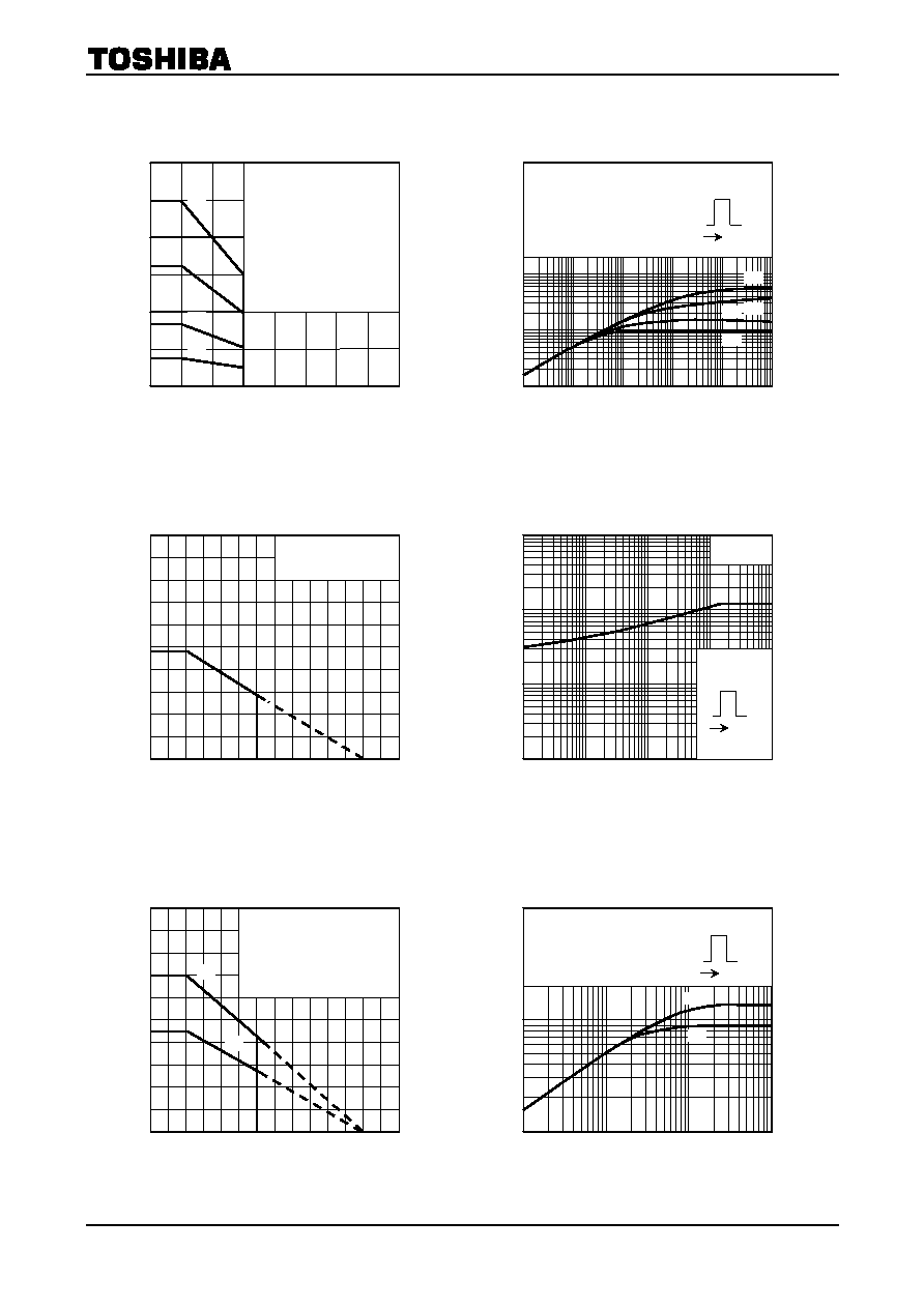
7
P
o
w
e
r
di
ssi
p
a
ti
on
P
D
(
W
)
T
r
a
n
sie
n
t t
h
e
r
m
a
l r
e
sistanc
e
R
th
(∞
C
/
W
)
Ambient temperature Ta (∞C)
TA7291AP
P
D
≠ Ta
P
o
w
e
r
di
ssi
p
a
ti
on
P
D
(
W
)
Pulse width t (s)
TA7291AP
t ≠ R
th
T
r
a
n
sie
n
t t
h
e
r
m
a
l r
e
sistanc
e
R
th
(∞
C
/
W
)
Ambient temperature Ta (∞C)
TA7291AS (J)
P
D
≠ Ta
P
o
w
e
r
di
ssi
p
a
ti
on
P
D
(
W
)
Pulse width t (s)
TA7291AS (J)
t ≠ R
th
Ambient temperature Ta (∞C)
TA7291AF
P
D
≠ Ta
Pulse width t (s)
TA7291AF
t ≠ R
th
T
r
a
n
sie
n
t t
h
e
r
m
a
l r
e
sistanc
e
R
th
(∞
C
/
W
)
(4)
(3)
(2)
(1)
(1) Infinite heat sink
Input pulse
(2) 80 cm
2
¥ 2 mm Al heat sink
(3) 25 cm
2
¥ 2 mm Al heat sink
(4) No heat sink
t (s)
P
W
30
10
5
3
1
50
100
10
-2
10
-1
1
10
10
2
10
3
0.1 1 10
100
1000
30
10
5
3
1
50
100
1000
500
300
Input pulse
t (s)
P
W
No heat sink
10
5
0
15
0 50 100
150
200
(2)
(1)
(3)
(4)
(1) Infinite heat sink
(2) 80 cm
2
¥ 2 mm Al
Heat sink (
qHS = 6∞C/W)
(3) 15 cm
2
¥ 2 mm Al
Heat sink (
qHS = 20∞C/W)
(4) No heat sink
qj-a = 65∞C/W
1.2
0.8
0
2.0
0.4
1.6
No heat sink
qj-a = 130∞C/W
0 50
100
150
175
25
75
125
1.2
0.8
0
2.0
0.4
1.6
(1) When mounted on a PCB
(PCB area: 60 mm
¥ 30 mm ¥
1.6 mm, Cu area: 50% or more)
(2) No heat sink
qj-a = 140∞C/W
0 50
100
150
175
25
75
125
(2)
(1)
1
10
100
1000
50
30
100
200
(1) No heat sink
(2) When mounted on a PCB
(PCB area: 60 mm
¥ 30 mm ¥ 1.8
mm, Cu area: 50% or more)
t (s)
P
W
(1)
(2)
10
Input pulse

TA7291AP/AS(J)/AF
2003-02-14
8
I
OUT
(A)
TA7291AP
V
CE (SAT)
≠ I
OUT
(Upper)
V
CE (SA
T
)
(V
)
I
OUT
(A)
TA7291AP
V
CE (SAT)
≠ I
OUT
(Lower)
V
CE (SA
T
)
(V
)
V
ref
≠ V
OUT
(H)
0 0.4 0.8
1.2
1.6
2.0
1.6
0.8
0
2.4
3.2
0 0.4 0.8
1.2
1.6
2.0
1.6
0.8
0
2.4
3.2
V
OUT
(H)
(V
)
V
ref
(V)
8
4
0
12
2
6
10
0 2 4
6
8
10
12
Resistor 10
W
Resistor 40
W
7/2/11 8/6/15
5/9/7
6/1/9
5 V
V
CC
2/7/4
4/8/5
1/5/1
12 V
V
S
G
V
ref
IN1
IN2
OUT1
V
S
= 12 V
V
CC
= 5 V
V
10
W
40
W
The heat fin of the TA7291AF
is connected to ground.
Open
Test circuit
Output open
V
S
≠ V
OUT
(H)
V
OUT
(H)
(V
)
V
S
(V)
12
9
6
10
7
8
8
9
10
11
7/2/11 8/6/15
5/9/7
6/1/9
5 V
V
CC
2/7/4
4/8/5
1/5/1
V
S
V
S
G
V
ref
IN1
IN2
OUT1
V
ref
= 8.0 V
V
CC
= 5.0 V
V
10
W
40
W
The heat fin of the TA7291AF
is connected to ground.
Open
Test circuit
8 V
V
CC
Output open
Resistor 40
W
Resistor 10
W
TA7291AP/AS(J)/AF
2003-02-14
9
Notes
∑
Power On/Off
At power on, V
CC
must be applied simultaneously or before V
S
. At power off, V
CC
must be removed
simultaneously or after V
S
.
∑
Input Circuit
A logic high on the V
IN
pin activates the input
circuit as shown in the figure.
When a voltage greater than or equal to V
IN
(high)
is applied to the pin, the circuit is active. When a
voltage less than or equal to V
IN
(low) is applied to
the pin or the pin is grounded, the circuit is
inactive.
When the pin is high, the input current I
IN
flows
into the input circuit. So, be careful about the
output impedance of the first stage.
The input hysteresis is 0.7 V (typ.). At power on
(V
CC
), set both input pins IN1 and IN2 to low.
∑
Output Circuit
Output high voltage
∑ Operation based on the V
ref
voltage
The V
ref
voltage is increased by twice the value
of V
BE
(small signal) in the V
ref
circuit. Then,
the voltage is applied to the base A of Q2 (power
transistor 2). As a result, the voltage which is
reduced by the value of V
BE
(Q2) appears on the
V
OUT
pin.
V
OUT
= V
ref
+ 2V
BE
V
BE
(
Q
2)
~
-
V
ref
+ 0.7 V
∑ V
ref
pin
The V
ref
pin must not be left open when unused.
In this case, connect it via a protection resistor
(3 kW or more) to the V
S
pin. Otherwise, it
might cause oscillation.
V
ref
must be £ V
S
.
Protection Features
Overcurrent Protection Circuit
The overcurrent protection circuit detects a current flowing through the upper power transistor. If the
current exceeds a predetermined value (about 2.5 A), the circuit turns all the power transistors off.
However, it does not always prevent overcurrent. If an output pin is shorted or grounded, the IC might be
destroyed before operation of the overcurrent protection circuit. So, be sure to connect a resistor or fuse to
the power supply (V
S
) line. (See "Application Circuit.")
Thermal Shutdown Circuit
If the chip temperature exceeds a predetermined limit (about 170∞C), the thermal shutdown circuit turns
all the power transistors off.
or
V
IN
6/1/9
4.
5 k
W
5/9/7
1 k
W
10 k
W
10 k
W
1.
3 k
W
1/5/1
V
IN
5 k
W
V
CC
standby
TA7291AP/TA7291AS (J)/TA7291AF
or
A
1/5/1
V
OUT
Q
1
10/3/13
2/7/4
4/8/5
8/6/15
V
ref
V
ref
circuit
Q
2
TA7291AP/TA7291AS (J)/TA7291AF

TA7291AP/AS(J)/AF
2003-02-14
10
Application Circuit
Note 1: Select the optimum value for the capacitor by experiment.
Note 2: Insert the current limiting resistor R1 to protect the IC from overcurrent.
Note 3: When V
S
= V
ref
, insert the resistor R2 (3 k
W or more) to protect the V
ref
pin from being damaged by a
surge.
Note 4: The IC may be destroyed due to short circuit between output pins, an output pin and V
CC
, or an output pin
and ground. Design the output line, V
CC
(V
M
, V
S
, V
EE
) lines and the ground line with great care.
Note
∑ Shoot-through current occurs when the mode is switched. The driver must enter the stop mode for
approximately 100 ms before switching between CW and CCW modes, or CW/CCW and brake modes.
∑ The proper IC functions are not guaranteed at power on/off. Before using the IC, check that any IC malfunctions
that are possible at power on/off will not cause a problem in the IC application.
TA7291AP/TA7291AS (J)/TA7291AF
7/2/11
1/5/1
8/6/15
10/3/13
4/8/5
2/7/4
GND
IN2
TA7291P/S/F
6/1/9
V
CC
V
S
IN1
5/9/7
R1 (Note 2)
(Note 1)
M
10
m
F
R2 (Note 3)
TA7291AP/AS(J)/AF
2003-02-14
11
Package Dimensions
Weight: 2.47 g (typ.)

TA7291AP/AS(J)/AF
2003-02-14
12
Package Dimensions
Weight: 0.92 g (typ.)
TA7291AP/AS(J)/AF
2003-02-14
13
Package Dimensions
Weight: 0.50 g (typ.)
TA7291AP/AS(J)/AF
2003-02-14
14
∑ TOSHIBA is continually working to improve the quality and reliability of its products. Nevertheless, semiconductor
devices in general can malfunction or fail due to their inherent electrical sensitivity and vulnerability to physical
stress. It is the responsibility of the buyer, when utilizing TOSHIBA products, to comply with the standards of
safety in making a safe design for the entire system, and to avoid situations in which a malfunction or failure of
such TOSHIBA products could cause loss of human life, bodily injury or damage to property.
In developing your designs, please ensure that TOSHIBA products are used within specified operating ranges as
set forth in the most recent TOSHIBA products specifications. Also, please keep in mind the precautions and
conditions set forth in the "Handling Guide for Semiconductor Devices," or "TOSHIBA Semiconductor Reliability
Handbook" etc..
∑ The TOSHIBA products listed in this document are intended for usage in general electronics applications
(computer, personal equipment, office equipment, measuring equipment, industrial robotics, domestic appliances,
etc.). These TOSHIBA products are neither intended nor warranted for usage in equipment that requires
extraordinarily high quality and/or reliability or a malfunction or failure of which may cause loss of human life or
bodily injury ("Unintended Usage"). Unintended Usage include atomic energy control instruments, airplane or
spaceship instruments, transportation instruments, traffic signal instruments, combustion control instruments,
medical instruments, all types of safety devices, etc.. Unintended Usage of TOSHIBA products listed in this
document shall be made at the customer's own risk.
∑ The products described in this document are subject to the foreign exchange and foreign trade laws.
∑ The information contained herein is presented only as a guide for the applications of our products. No
responsibility is assumed by TOSHIBA CORPORATION for any infringements of intellectual property or other
rights of the third parties which may result from its use. No license is granted by implication or otherwise under
any intellectual property or other rights of TOSHIBA CORPORATION or others.
∑ The information contained herein is subject to change without notice.
000707EBA
RESTRICTIONS ON PRODUCT USE