 | –≠–ª–µ–∫—Ç—Ä–æ–Ω–Ω—ã–π –∫–æ–º–ø–æ–Ω–µ–Ω—Ç: TA76432F | –°–∫–∞—á–∞—Ç—å:  PDF PDF  ZIP ZIP |

TA76432FT/FC/F/FR/S
2002-07-12
1
TOSHIBA Bipolar Linear Integrated Circuit Silicon Monolithic
TA76432FT,TA76432FC,TA76432F,TA76432FR,TA76432S
1.26-V Adjustable High-Precision Shunt Regulators
These devices are adjustable high-precision shunt regulators
whose output voltage (V
KA
) can be set arbitrarily using two
external resistors.
These devices have a precise internal reference voltage of 1.26 V,
enabling them to operate at low voltage.
These devices are ideal for use as error amplifiers in 3-V
switching-regulator systems. In addition, they can be used as
zener diodes to perform temperature compensation.
Features
∑ Precision reference voltage: V
REF
= 1.26 V ± 1.4% (Ta = 25∞C)
∑ Small temperature coefficient: |V
REF
| = 30 ppm/∞C (typ.)
∑ Adjustable output voltage: V
REF
V
OUT
19 V
∑ Minimum cathode current for regulation:
I
kmin
= 0.5 mA (max.)
∑ Operating temperature: Ta = -40~85∞C
∑ Packages: UFV (TA76432FT), SMV (TA76432FC),
PW-MINI (TA76432F/FR) and
TO-92MOD
(TA76432S)
∑ The TA76432FT is housed in an ultra-thin UFV package.
(thickness: 0.7 mm typ.)
TA76432FT
TA76432FC
TA76432F/FR
TA76432S
Weight
SSOP5-P-0.65C : 0.007 g (typ.)
SSOP5-P-0.95 : 0.014 g (typ.)
HSOP3-P-1.50 : 0.05 g (typ.)
SSIP3-P-1.27
: 0.36 g (typ.)

TA76432FT/FC/F/FR/S
2002-07-12
2
Pin Assignment/Marking
TA76432FT/TA76432FC
TA76432F/FR
No. TA76432F TA76432FR
1
CATHODE (K) REFERENCE
(REF)
2 ANODE
(A)
ANODE
(A)
3 REFERENCE
(REF)
CATHODE (K)
Note: TA76432F vs. TA76432FR: reverse
pin connection.
How to Order
Product No.
Package Type
Packing Type and Capacity
Minimum Order
TA76432FT (TE85L)
UFV
(surface-mount type)
Embossed tape: 3000/tape
1 tape
TA76432FC (TE85L)
SMV
(surface-mount type)
Embossed tape: 3000/tape
1 tape
TA76432F/R
On cut tape (TE12L): 100/tape section
100
TA76432F/R (TE12L)
PW-MINI (SOT-89)
(surface-mount type)
Embossed tape: 1000/tape
1 tape
TA76432S
Loose in bag: 200/bag
1 bag
TA76432S (TPE6)
TO-92MOD
(lead type)
Radial tape: 2000/tape
1 tape
Note: The lead pitch for the TA76432S and TA76432S (TPE6) may vary.
Functional Block Diagram
Circuit Symbol
Cathode (K)
Reference (REF)
Anode (A)
1.26 V
Anode (A)
Cathode (K)
Reference (REF)
1: REFERENCE (REF)
2: ANODE (A)
3: CATHODE (K)
Lot No: Last decimal digit of the year of manufacture and January
to December is denoted by alphabet A to L respectively.
For example: Jan-2001 coded to "1A"
TA76432S
TA76
1
2
3
432S
1: NC
2: ANODE (A)
3: CATHODE (K)
4: REFERENCE (REF)
5: ANODE (A)
2 F
5 4
1 3
2
1
3
2
Lot No. (three-digit number)
Type marking
(two-digit number)
Lot No.
Þ
The week of manufacture
Þ
The year of manufacture
(last decimal digit of the year of
manufacture)
∑ TA76432F: AU
∑ TA76432FR: BU

TA76432FT/FC/F/FR/S
2002-07-12
3
Typical Application Circuits
Precautions during Use
(1) TA76432FT, TA76432FC, TA76432F/FR, TA76432S
These products contain MOS elements. Please take care to avoid generating static electricity when
handling these devices.
(2) TA76432FT, TA76432FC, TA76432F/FR, TA76432S
The oscillation frequency of these devices is determined by the value of the capacitor connected between
the anode and the cathode.
When establishing maximum operating condition parameters, please derate the maximum rating values
specified in these datasheets so as to allow an operational safety margin.
Use of a laminated ceramic capacitor is recommended.
(3) Precautions when handling anode pin of TA76432FT/TA76432FC
Pin 2 and pin 5 should normally be shorted together. If only pin 5 is used, pin 2 should either be left open
or always kept at a lower potential than pin 5. Do not leave pin 5 open and use pin 2 only.
Maximum Ratings
(Ta
=
=
=
=
25∞C)
Characteristics Symbol
Rating
Unit
Cathode voltage
V
KA
20 V
Cathode current
I
K
20
mA
Cathode-anode reverse current
-
I
K
10
mA
Reference voltage
V
REF
7 V
Reference current
I
REF
50
m
A
Reference-anode reverse current
-
I
REF
10 mA
TA76432FT
0.45
(Note
1)
0.2
TA76432FC
0.38
(Note
2)
TA76432F/FR 0.5
Power dissipation
TA76432S
P
D
0.8
W
TA76432FT
277
(Note
1)
625
TA76432FC
328
(Note
2)
TA76432F/FR 250
Thermal resistance
TA76432S
R
th
156
∫C/W
Operating temperature
T
opr
-
40
~
85 ∫C
Junction temperature
T
j
150
∫C
Storage temperature
T
stg
-
55
~
150 ∫C
Note 1: Glass epoxy substrate mounting: 30 mm
¥
30 mm
¥
0.8 mmt (Cu pad area 35 mm
2
)
Note 2: Glass epoxy substrate mounting: 30 mm
¥
30 mm
¥
0.8 mmt (Cu pad area 50 mm
2
)
1.26 V Reference (V
KA
=
V
REF
)
V
OUT
=
1.26 V
V
IN
Shunt regulator (V
KA
>
V
REF
)
V
IN
V
OUT
R1
I
R
R
1
V
REF
2
1
REF
◊
+
˜
˜
¯
ˆ
Á
Á
Ë
Ê
+
=
V
OUT
R1
R2
V
REF
TA76432FT/FC/F/FR/S
2002-07-12
4
Recommended Operating Conditions
Characteristics Symbol
Min
Typ.
Max
Unit
Cathode voltage
V
KA
V
REF
æ
19 V
Cathode current
I
K
0.5
æ
15 mA
Operating temperature
T
opr
-
40
æ
85 ∞C
Electrical Characteristics
(Unless otherwise specified, Ta
=
=
=
=
25∞C, I
K
=
=
=
=
5 mA)
Characteristics Symbol Test
Condition Min
Typ.
Max
Unit
Reference voltage
V
REF
V
KA
=
V
REF
1.242
1.26
1.278
V
Deviation of reference input voltage
over temperature
V
REF (dev)
0∞C
<
=
Ta
<
=
85∞C, V
KA
=
V
REF
æ
3 15 mV
V
REF
<
=
V
KA
<
=
5 V
æ
0.5 2.5
Ratio of change in reference input
voltage to the change in cathode
voltage
D
V
REF
/
D
V
5 V
<
=
V
KA
<
=
19 V
æ
0.3 2.0
mV/V
Reference Input current
I
REF
V
KA
=
V
REF
æ
2 4
m
A
Deviation of reference input current
over temperature
I
REF (dev)
0∞C
<
=
Ta
<
=
85∞C, V
KA
=
V
REF
,
R
1
=
10 k
W
, R
2
=
•
æ
0.3 1.2
m
A
Minimum cathode current for
regulation
I
Kmin
V
KA
=
V
REF
æ
0.2 0.5 mA
Off-State cathode current
I
Koff
V
KA
=
19 V, V
REF
=
0 V
æ
æ
1.0
m
A
Dynamic impedance
Ô
Z
KA
Ô
V
KA
=
V
REF
, f
<
=
1 kHz,
0.5 mA
<
=
I
K
<
=
15 mA
æ
0.2 0.5
W
The deviation parameters V
REF (dev)
and I
REF (dev)
are defined as the maximum variation of the V
REF
and I
REF
over the
rated temperature range.
The average temperature coefficient of the V
REF
is defined as:
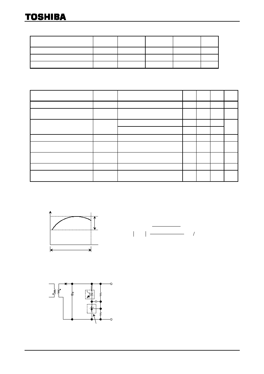
Application Circuit Example
Error amplification circuit for switching power supply
This circuit amplifies the difference between the switching power supply's secondary output voltage and the shunt
regulator's reference voltage. It then feeds the amplified voltage back to the primary input voltage via the
photocoupler.
C
ppm
Ta
C
@25
V
10
V
V
REF
6
(dev)
REF
REF
∞
D
˜
˜
˜
¯
ˆ
Á
Á
Á
Ë
Ê
∞
¥
=
a
min
max
V
REF (dev)
D
Ta
V
REF
Photo-
coupler
V
OUT
GND
Shunt regulator

TA76432FT/FC/F/FR/S
2002-07-12
5
C
a
th
od
e cu
rr
ent
I
K
(mA
)
Ambient temperature Ta (∞C)
P
Dmax
≠ Ta
A
l
l
o
w
abl
e p
o
w
e
r di
s
s
i
pati
o
n
P
Dmax
(W
)
Ambient temperature Ta (∞C)
P
Dmax
≠ Ta
A
l
l
o
w
abl
e p
o
w
e
r di
s
s
i
pati
o
n
P
Dmax
(W
)
Ambient temperature Ta (∞C)
P
Dmax
≠ Ta
A
l
l
o
w
abl
e p
o
w
e
r di
s
s
i
pati
o
n
P
Dmax
(W
)
Cathode voltage V
KA
(V)
I
K
≠ V
KA
Cathode voltage V
KA
(V)
I
K
≠ V
KA
C
a
th
od
e cu
rr
ent
I
K
(
m
A)
0.6
0
0.2
0.4
0.8
1.0
1.2
0 20 40 60
100
120
80
140
160
Mounted on ceramic substate
: 15
¥
15
¥
0.8 mm t
Ta
=
25∞C
TA76432F, FR
0.6
0
0.2
0.4
0.8
1.0
0 20 40 60
100
120
80
140
160
TA76432S
-
1.0
-
0.5 0 0.5
1.5
1.0
-
10
0
10
20
VKA
=
VREF
Ta
=
25∞C
Input VKA
IK
25∞C
85∞C
Ta
=
-
40∞C
-
1.0
-
0.5
0 0.5
1.5
1.0
200
-
100
0
100
300
25∞C
85∞C
85∞C
25∞C
Ta
=
-
40∞C
Ta
=
-
40∞C
IK min
VKA
=
VREF
Ta
=
25∞C
Input
VKA
IK
Ambient temperature Ta (∞C)
P
Dmax
≠ Ta
A
l
l
o
w
abl
e p
o
w
e
r di
s
s
i
pati
o
n
P
Dmax
(W
)
0.3
0
0.1
0.2
0.4
0.5
0.6
0 20 40 60
100
120
80
140
160
Mounted on glass epoxy substate
: 30
¥
30
¥
0.8 mm t
Cupper pad area: 50 mm
2
Ta
=
25∞C
TA76432FC
0.3
0
0.1
0.2
0.4
0.5
0.6
0 20 40 60
100
120
80
140
160
Mounted on glass epoxy substate
: 30
¥
30
¥
0.8 mm t
Cupper pad area: 35 mm
2
TA76432FT