 | –≠–ª–µ–∫—Ç—Ä–æ–Ω–Ω—ã–π –∫–æ–º–ø–æ–Ω–µ–Ω—Ç: TA8050F | –°–∫–∞—á–∞—Ç—å:  PDF PDF  ZIP ZIP |
TA8050F
2002-02-27
1
TOSHIBA Bipolar Linear Integrated Circuit Silicon Monolithic
TA8050F
1.5 A DC Motor Driver with Brake Function
The TA8050F is a 1.5 A motor driver which directly drives a
bidirectional DC motor. Inputs DI1 and DI2 are combined to
select one of forward, reverse, stop, and brake modes. Since the
inputs are TTL-compatible, this IC can be controlled directly from
a CPU or other control system. The IC also has various protective
functions.
Features
∑ Bidirectional DC motor driver
∑ Current capacity
: 1.5 A
∑ Four modes
: Forward, Reverse, Stop, and Brake
∑ Recommended operating supply voltage range
:
V
CC
= 6~16 V
∑ Protective functions : Thermal Shutdown, Short Circuit Protection, and Overvoltage Shutdown
∑ Built-in diode for counteracting counter electromotive force
∑ HSOP-20 Pin power flat package
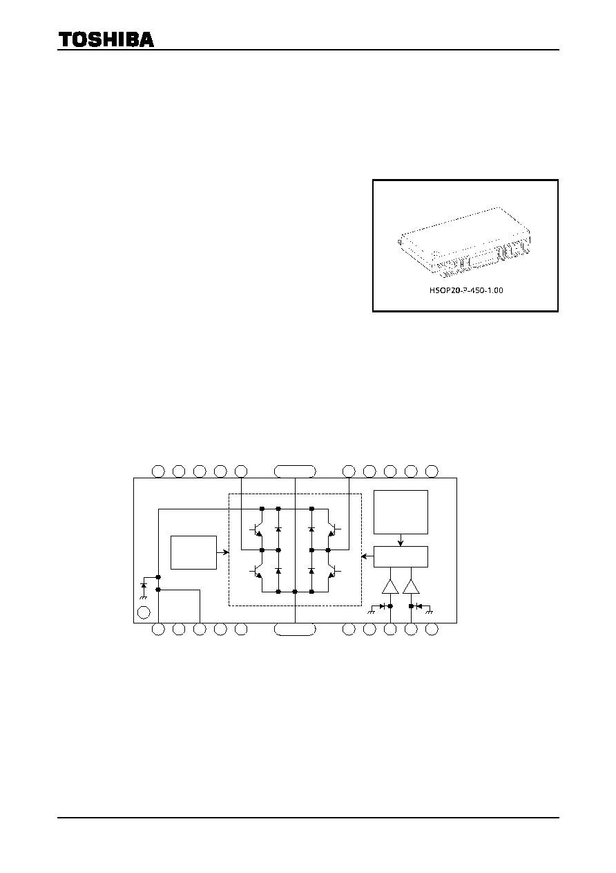
Block Diagram and Pin Layout
Weight: 0.79 g (typ.)
M (
-
)
16
FIN
15
Short
protection
20
17
18
19
5
1
4
3
2
11
12
13
14
6
10
9
8
7
FIN
Control logic
Thermal-
shutdown and
over-voltage
protection
M (
+
)
GND
GND
V
CC
V
CC
DI1 DI2

TA8050F
2002-02-27
2
Pin Description
Pin No.
Symbol
Description
1
3
V
CC
Power supply pin. This pin has a function to turn off the output when the applied voltage exceeds
27.5 V, thus protecting the IC and the load.
FIN GND
Grounded
8
9
DI1
DI2
Output status control pin.
Connects to a PNP-type voltage comparator.
15 M
(
+
)
Connects to the DC motor. Both the sink and the source have a current capacity of 1.5 A.
Diodes for absorbing counter electromotive force are contained on the V
CC
and GND sides.
16 M
(
-
)
Connects to the DC motor together with pin 15 and has the same function as pin 3. This pin is
controlled by the inputs from pins 8 and 9.
2, 4~7
10~14
17~20
NC
Not connected. (Electrically, this pin is completely open.)
Truth Table
Input/Output
Input Output
DI1 DI2 M
(
+
) M
(
-
)
H H L L
(Note
1)
L H L H
H L H L
L L
OFF
(high
impedance)
(Note
2)
Note 1: Brake mode comes into effect when both M (
+
) and M (
-
) go low.
Note 2: Stop mode comes into effect when both M (
+
) and M (
-
) turn OFF.
TA8050F
2002-02-27
3
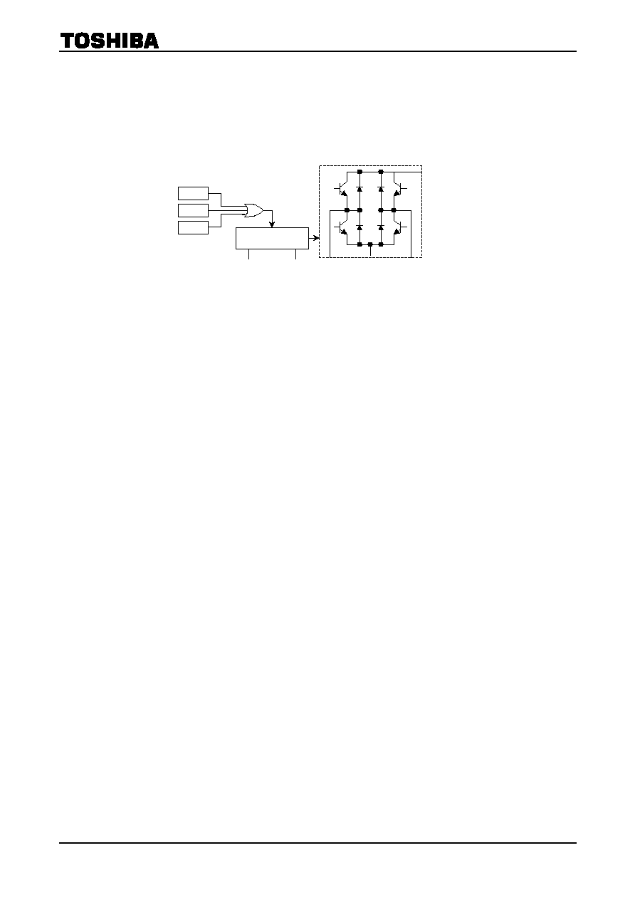
Description of Multi-Protective Operation
The TA8050F has functions for protection from overvoltage (V
SD
), overcurent (I
SD
), and overheat (T
SD
). These
functions protect the IC (and the motor load in some cases) from deterioration or destruction due to power-related
overstress.
The three functions work independently.
Each function is explained below.
1. Overvoltage protection (V
SD
)
Basic
operation
When the voltage supplied to the V
CC
pin is up to the V
SD
detection voltage, the output is controlled by
the input signals. However, when the V
CC
voltage exceeds the detection voltage, the output enters
high-impedance state regardless of the input signals.
Detailed
explanation
The V
SD
voltage is detected by comparing the Zener voltage with the voltage obtained by dividing V
CC
with a resistor. When the center voltage of the resistor is higher than the Zener voltage, a transistor-off
instruction is issued to the control logic. When it is lower than the Zener voltage, the logic is controlled
by the input signals from DI1 and DI2.
2. Overheat protection (T
SD
)
Basic
operation
When the junction (chip) temperature is up to the T
SD
detection temperature, the output is controlled
by the input signals. When it exceeds the T
SD
detection temperature, the output enters high-impedance
state regardless of the input signals.
Detailed
explanation
The temperature is detected by monitoring V
F
of a diode on the chip. When the diode V
F
is lower than
the internal reference voltage, an output transistor-off instruction is issued to the control logic. When it
is higher than the internal reference voltage, the logic is controlled by the input signals from DI1 and
DI2.
DI1
DI2
CONTROL LOGIC
V
SD
M (
-
)
M (
+
)
I
SD
T
SD
TA8050F
2002-02-27
4
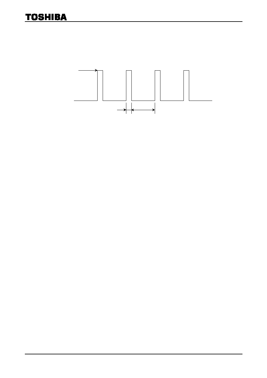
3. Overcurrent protections (I
SD
)
∑
∑
∑
∑ Basic
operation
When the output current (M (+) or M (-)Isink or Isource) is up to the I
SD
detection current, the output
is controlled by the input signals. When it exceeds the detection current, the output assumes a
switching waveform as shown in Figure 1.
Detailed
explanation
The output current is detected by monitoring the V
BE
from each output transistor. One detection circuit
connects to one of the output transistors and leads to the short-circuit protection circuit. When a
current exceeding the I
SD
detection current flows through one of the four output transistors, the
short-circuit protection circuit is activated. This circuit contains a timer. When overcurrent condition
continues for 20 ms (typically) , the protection circuit places the output in high-impedance mode and, 80
ms (typically) later, returns the IC to ON mode. The switching-waveform output is repeated until
overcurrent condition is no longer present.
ON
ISD or more
20
m
s Typ.
80
m
s Typ.
ON
ON
ON
OFF
OFF
OFF
Figure 1 Basic operation

TA8050F
2002-02-27
5
Maximum Ratings
(Ta
=
=
=
= 25∞C)
Characteristics Symbol
Rating
Unit
V
CC
30
Supply voltage
V
CC
60 (1 s)
V
Input voltage
V
IN
-
0.3~V
CC
V
Output current
I
O∑AVE
1.5 A
Operation temperature
T
opr
-
40~110 ∞C
Storage temperature
T
stg
-
55~150 ∞C
Lead temperature time
T
sol
260
(10
s)
∞C
HSOP20-P-450-1.00 Thermal Resistance Data
(Ta
=
=
=
= 25∞C)
Characteristics Rating Unit
Test
Condition
R
q
j-a 125
∞C/W
æ
R
q
j-c 13
∞C/W
æ
PD1
1.0
W
Without radiation board
PD2 1.5
W
60
¥
30
¥
1.6 mm 50%Cu mounted
PD3 3.2
W
50
¥
50
¥
1.0 mm Iron board mounted
PD4
9.6
W
Infinite radiation board mounted
Electrical Characteristics
(Unless otherwise specified, V
CC
=
=
=
= 6~16 V, Tc ==== ----40~110∞C)
Characteristics Symbol
Pin
Test
Circuit
Test Condition
Min
Typ.
Max
Unit
I
CC1
æ
Stop
æ
8 15
I
CC2
æ
Forward/Reverse
æ
27 50
Current consumption
I
CC3
V
CC
æ
Brake
æ
16 30
mA
V
IL
æ
æ
æ
æ
0.8
Input voltage
V
IH
DI1/DI2
æ
æ
2.0
æ
æ
V
I
IL
æ
V
IN
=
0.4 V
æ
æ
-
100
Input current
I
IH
DI1/DI2
æ
V
IN
=
V
CC
æ
æ
100
m
A
æ
I
O
=
1.5 A, Tc
=
25∞C
æ
2.2 2.9
Output saturation voltage
V
sat (total)
M
(
+
)/M (
-
)
æ
I
O
=
1.5 A, Tc
=
110∞C
æ
2.2 2.8
V
I
LEAK-U
æ
V
O
=
0 V
æ
æ
-
100
Output leakage current
I
LEAK-L
M (
+
)/M (
-
)
æ
V
O
=
V
CC
æ
æ
100
m
A
V
F-U
æ
2.6
æ
Diodes forward voltage
V
F-L
M (
+
)/M (
-
)
æ
I
F
=
1.5 A
æ
1.5
æ
V
Over-current detection
I
SD
æ
æ
1.8
3
4
A
Shutdown temperature
T
SD
æ
æ
æ
150
æ
∞C
Over-voltage detection
V
SD
æ
æ
25 27.5 30 V
t
PLH
æ
æ
æ
1 10
Transfer delay time
t
PHL
æ
æ
æ
1 10
m
S
Note 3: The parameter values above are guaranteed in the operating voltage rage of 6 V to 16 V. If the guaranteed
range is exceeded in practical use, make sure that the IC operates normally in application.

TA8050F
2002-02-27
6
I/O Equivalent Circuit
V
CC
GND
15
M (
+
)
16
M (
-
)
Control logic
Short protection
circuit
8
DI1
9
DI2
Thermal shutdown
and overvoltage
protection circuits
FIN
1, 3
TA8050F
2002-02-27
7
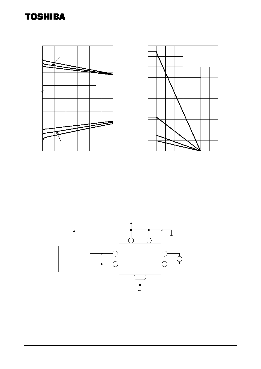
Example of Application Circuit
Output current I
OUT
(A)
V
OL
, V
OH
≠ I
OUT
V
OL
(
V
)
O
u
t
p
u
t
s
a
t
u
r
a
t
i
o
n
v
o
l
t
a
g
e
V
OH
(V
)
Ambient temperature Ta (∞C)
P
D
MAX ≠ Ta
Max
i
mu
m p
o
w
e
r di
s
s
i
pati
o
n
P
D
MA
X
(W
)
0
0
0.5
1.0
1.5
1.0
1.5
1.5
1.0
0
0.5
2.0
0.5
25∞C
110∞C
-
40∞C
25∞C
110∞C
-
40∞C
0
0
50
100
150
200
2
4
6
8
10
(1) Infinite radiation board
(2) 50
¥
50
¥
1.0 mm Fe
(3) 60
¥
30
¥
1.6 mm
Cu 50% PCB board
(4) No radiation board
(1)
(2)
(3)
(4)
15
16
1
3
9
8
M
FIN
*
: Connect this capacitor as close to the
IC as possible.
5 V
TA8050F
+
V
GND
M (
-
)
V
DD
V
SS
DI1
DI2
OUTPUT
PORT1
PORT2
V
CC
V
CC
M (
+
)
*
C1
10
m
F
Microprocessor
TA8050F
2002-02-27
8
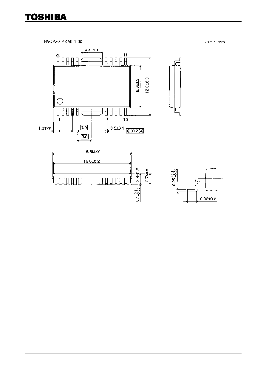
Package Dimensions
Weight: 0.79 g (typ.)

TA8050F
2002-02-27
9
∑
TOSHIBA is continually working to improve the quality and reliability of its products. Nevertheless, semiconductor
devices in general can malfunction or fail due to their inherent electrical sensitivity and vulnerability to physical
stress. It is the responsibility of the buyer, when utilizing TOSHIBA products, to comply with the standards of
safety in making a safe design for the entire system, and to avoid situations in which a malfunction or failure of
such TOSHIBA products could cause loss of human life, bodily injury or damage to property.
In developing your designs, please ensure that TOSHIBA products are used within specified operating ranges as
set forth in the most recent TOSHIBA products specifications. Also, please keep in mind the precautions and
conditions set forth in the "Handling Guide for Semiconductor Devices," or "TOSHIBA Semiconductor Reliability
Handbook" etc..
∑
The information contained herein is presented only as a guide for the applications of our products. No
responsibility is assumed by TOSHIBA CORPORATION for any infringements of intellectual property or other
rights of the third parties which may result from its use. No license is granted by implication or otherwise under
any intellectual property or other rights of TOSHIBA CORPORATION or others.
∑
The information contained herein is subject to change without notice.
000707EAA_S
RESTRICTIONS ON PRODUCT USE