TA8493F/AF/BF
2002-01-31
1
Toshiba Bipolar Linear Integrated Circuit Multi-Chip
TA8493F, TA8493AF, TA8493BF
3-Phase Full Wave Brushless DC Motor Driver IC for CD-ROM Drives
These 3-phase, full-wave, brushless DC motor driver ICs have
been developed for use in CD-ROM drive spindle motors. The
TA8493F/ AF/ BF contain in its upper stage a discrete power
transistor (P-ch-MOS) and uses direct PWM control system,
which enables the IC to provide superior thermal efficiency.
Furthermore, the multi-chip structure of this device facilitates
dispersion of the heat generated inside the package, making it
possible to suppress heat concentration.
Features
∑ Multi-chip structure (3 ◊ 2SJ465 chips built-in)
∑ Direct PWM control system
∑ Drive system: 120∞drive system (TA8493F/BF)
:
180∞drive system (TA8493AF)
∑ Built-in current limiter: I
LIM
= 0.7 A (typ.) (at R
F
= 0.33 )
∑ Built-in reversing brake/short brake functions
∑ FG signal output (using hall element output signal)
∑ Built-in hall bias
∑ Built-in thermal shutdown circuit
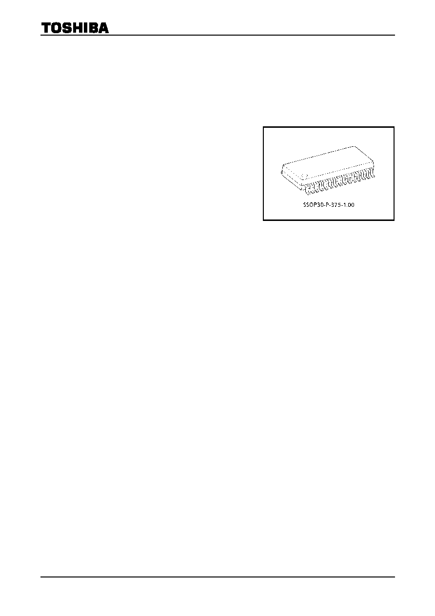
∑ Package: MFP-30
Weight: 0.63 g (typ.)

TA8493F/AF/BF
2002-01-31
3
PIN Assignment
Terminal
No.
Terminal
Symbol
Function Remarks
1 L
b
(G)
b-phase upper side power transistor (base)
output terminal
Keep open.
2 L
a
(G)
a-phase upper side power transistor (base)
output terminal
Keep open.
3 L
a
a-phase output terminal
Connect to the coil.
4 V
M2
Supply voltage terminal for motor drive
Connect to V
M1
externally.
5
SB
RUN/STOP control terminal
H: RUN, L: STOP
6 R
F1
Output current detection terminal
Sets limiter current value.
Connect to R
F2
externally and between this
terminal and GND.
7 GND2
GND
æ
8 C
RF
Output current filter terminal
Connect a capacitor between this terminal
and GND.
9 N.C.
10
FGO
FG amplifier output terminal
Outputs a signal whose frequency is
determined by the CD rotation frequency.
11
BRK
Brake mode select terminal
Output mode when V
C
>
V
ref
12 H
b
-
b-phase negative hall signal input terminal
Connect to hall element output terminal.
13 H
b
+
b-phase positive hall signal input terminal
Connect to hall element output terminal.
14 H
a
-
a-phase negative hall signal input terminal
Connect to hall element output terminal.
15 H
a
+
a-phase positive hall signal input terminal
Connect to hall element output terminal.
16 H
c
+
c-phase positive hall signal input terminal
Connect to hall element output terminal.
17 H
c
-
a-phase negative hall signal input terminal
Connect to hall element output terminal.
18 HB
Hall
element
bias
terminal
Open collector output. Connect to the
negative side of hall element bias line.
19 C
d
Forward/reverse changeover gain
adjustment terminal
Adjust a rotation direction changeover gain
20 V
CC
Supply voltage terminal for control circuits
V
CC (opr)
=
4.5 to 5.5 V
21 V
C
Control amplifier input terminal
Use the control signal as input.
22 V
ref
Control amplifier reference voltage input
terminal
Use the reference voltage for the control
amplifier as input.
23
OSC
Triangular wave oscillation terminal
Connect a capacitor between this terminal
and GND.
24 GND1
GND
æ
25 R
F2
Output current detection terminal
Sets limiter current value.
Connect to R
F1
externally and between this
terminal and GND.
26
MS
Mode select terminal
Determines output mode.
27 L
c
(G)
c-phase upper side power transistor (base)
output terminal
Keep open.
28 L
c
c-phase output terminal
Connect to the coil.
29 V
M1
Supply voltage terminal for motor drive
Connect to V
M2
externally.
30 L
b
b-phase output terminal
Connect to the coil.

TA8493F/AF/BF
2002-01-31
5
Characteristics Symbol
Test
Circuit
Test Condition
Min
Typ.
Max
Unit
Output
Resistance
(upper side)
R
ON (U)
I
O
=
0.6 A
æ
0.5 1.0
W
Saturation
Voltage
(lower side)
V
SAT (L)
4
I
O
=
0.6 A
æ
0.4 0.8 V
Cut-off Current
(upper side)
I
L (U)
V
L
=
16 V
æ
æ
10
Output Circuit
Cut-off Current
(lower side)
I
L (L)
5
V
L
=
16 V
æ
æ
10
m
A
Input Voltage (H)
V
MS (H)
CCW mode
V
C
>
V
ref
, BRK: L
3.0
æ
V
CC
Input Voltage (L)
V
MS (L)
Reversing brake mode
V
C
>
V
ref
, BRK: L
æ
æ
0.5
V
Mode Select
Circuit
Input Current
I
INMS
6
V
MS
=
GND, (source current)
æ
æ
1
m
A
Hysteresis
Voltage
V
HYS
8
æ
5
20
45
mV
p-p
Output Voltage
(H)
V
OFG (H)
Source
current:
10
m
A
V
CC
-
0.5
æ
æ
FG Amp.
Output Voltage
(L)
V
OFG (L)
7
Sink current: 10
m
A
æ
æ
0.5
V
Input Voltage (H)
V
BRK (H)
æ
3.0
æ
V
CC
Input Voltage (L)
V
BRK (L)
æ
æ
æ
0.5
V
Short Brake
Circuit
Input Current
I
INBRK
6
V
BRK
=
GND, (source current)
æ
æ
1
m
A
Triangular
Oscillation Circuit
Oscillation
Frequency
f
OSC
æ
C
=
560 pF
(Note2)
æ
39
æ
kHz
Thermal Shut-down Operating
Temperature
TSD
æ
Junction temperature
(according to design
specification)
(Note2)
æ
175
æ
∞C
Note2: this is not tested.

