 | –≠–ª–µ–∫—Ç—Ä–æ–Ω–Ω—ã–π –∫–æ–º–ø–æ–Ω–µ–Ω—Ç: TB1239BF | –°–∫–∞—á–∞—Ç—å:  PDF PDF  ZIP ZIP |
TB1239BF
2002-02-12
1
Bi-CMOS Integrated Circuit Silicon Monolithic
TB1239BF
Luminance, Chroma and Synchronizing Signals Processor IC for PAL/NTSC/SECAM
COLOR TV
TB1239BF integrates luminance, chroma and synchronizing
signals processing circuits for PAL/NTSC/SECAM color TV
system.
TB1239BF incorporates high performance picture quality
compensation circuits in luminance section, an automatic
PAL/NTSC/SECAM discrimination and decode circuits in chroma
section, and an automatic 50/60 Hz discrimination circuit in
synchronizing section.
Besides a crystal oscillator generates 4.43 MHz, 3.58 MHz and
M/N-PAL clock signals internally for color demodulation. A
horizontal PLL circuit is also built in this IC.
PAL/SECAM demodulation circuits which are adjustment-free
circuits incorporates a 1 H DL circuit inside for operating the
base band signal processing system.
Also, TB1239BF makes it possible to set and to control various functions through the built-in I
2
C BUS line.
Features
Luminance Section
∑ Built-in chroma trap filter
∑ Black stretch circuit
∑ DC restoration circuit
∑ Y delay line
∑ Sharpness control
∑ Sub-Contrast control (-/+2dB)
∑ Black set-up for PAL plus
Chroma Section
∑ Built-in 1 H delay circuit (PAL/SECAM base band demodulation system)
∑ One crystal color demodulation circuit (4.43 MHz, 3.58 MHz, M/N-PAL)
∑ Automatic system discrimination system and forced system mode
∑ 1 H delay line also serves as comb filter in NTSC demodulation
∑ Built-in band-pass and take-off filter, SECAM bell filter
∑ Sub-Color control (-/+2dB)
Synchronizing Section
∑ Built-in horizontal VCO resonator
∑ Adjustment-free horizontal and vertical oscillation by count-down circuit
∑ Automatic vertical frequency discrimination circuit
∑ Noise detection circuit
Weight: 0.83 g (typ.)
Preliminary

TB1239BF
2002-02-12
2
Others
∑ Y/C out level control
∑ 4-channels inputs switching
∑ 2-input circuit for RGB
∑ 2-input circuit for Y/Cb/Cr
∑ Y/Cb/Cr outputs
∑ Cb/Cr offset adjustment
∑ Built-in pre filters for A/D converter

TB1239BF
200
2-
02-
1
2
3
B
l
ock D
i
agr
a
m
YS1
B1-I
N
Cl
am
p
Ma
t
r
i
x
Cl
am
p
Of
f
s
et
2
CW
P
has
e
VC
X
O
FSC
Tint
APC
S
ub-
Col
o
r
B
a
s
eband SW
LP
F
SW
(
C-m
u
t
e
)
P/N
DE
M
O
BPF
/
TOF
AC
C
C
VBS
/YC
Se
le
c
t
Cl
am
p
Ma
t
r
i
x
1 H DL
P/N
ID
SW
Half Tone
SW
Offs
et1
Cb/
C
r
SW
Y
S
ub-
c
ont
rast
Y D
L
EQ
S
Doubel
Tr
a
p
Se
ca
m
DE
M
O
BEL
L
Bla
c
k
AD
J
Se
ca
m
ID
DE
-
Em
p
hasi
s
Col
o
r
S
y
ste
m
C
Y
Chrom
a
ID
Chrom
a
Tr
a
p
Set
-up
Amp
LPF
CLP
Sharp-
ness
DL
Clam
p
I
2
C B
u
s Cont
rol
V C
/
D
V
SE
PA
V
IN
TEG
H C/
D
H V
C
O
AFC
MASK
Sy
n
c
SE
PA
SW
G1-IN
R1-IN
Y/C-G
ND
CR2-IN
CB2-I
N
Y2-I
N
Y/C-V
CC
B2-I
N
G2-IN
R2-IN
YS2/Y
M
FIL
X'tal
SDA
SCL
SYNC
-V
CC
YVI-
OU
T
SCP
HS
DIGI
TA
L-GND
DIGI
TA
L-V
DD
COMB
C-IN
/FOR
CE
D-S
VS
CVB
S-OU
T
SYNC
-IN
CVBS1
/Y1
-IN
COMB
Y-I
N
CR-OUT
CB
-OUT
Y-
O
U
T
CLP
-
F
I
L
Y1
-
I
N
CB
1-I
N
CR1-I
N
S
Y
NC-GND
YS3
C3-I
N
APC
-
F
IL
CV
B
S
3
/
Y
3
-
I
N
A
DDRE
S
S
C2-I
N
CV
B
S
2
/
Y
2
-
I
N
COM
B
SY
S
FSC
-
OU
T
AFC
-
FIL
C1-I
N
39
40
41
42
43
44
45
46
47
48
1
2
3
4
5
7
6
8
9
10
11
12
13
14
24
23
22
21
20
19
18
17
16
15
38
37
36
35
34
32
33
31
30
29
28
27
26
25
+

TB1239BF
2002-02-12
4
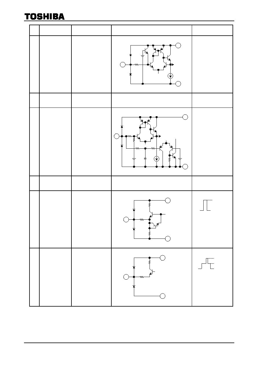
Terminal Descriptions
(YC
-
-
-
-
V
CC
/SYNC
-
-
-
-
V
CC
/D
-
-
-
-
V
DD
=
=
=
=
5 V and Ta
=
=
=
=
25∞C, unless otherwise specified)
Pin
No.
Pin Name
Function
Interface Circuit
Input/Output Signals
1 CVBS1/Y1-IN
Input CVBS1/Y1 signal
through a clamping
capacitor.
CVBS: 1 V
p-p
Y: 1 V
p-p
(with sync)
DC: 1.8 V
2 SYNC-IN
Input signal to
synchronize.
1 V
p-p
(with sync)
DC: 1.7 V
3 CVBS-OUT
CVBS or Y
+
C signal
output pin.
2 V
p-p
(with sync)
DC: 0.6 V
4 VS
Output pin of vertical
synchronizing signal.
Minimun pull-up resister
is 6.8 k
W
.
4.7 V
<
=
Hi
<
=
5.2 V
0 V
<
=
Low
<
=
0.8 V
3
32
28
700
m
A
8 k
W
50
W
100
W
4
12
16
50
W
120
m
A
Hi
Low
1
32
28
50
m
A
50
m
A
2.
5 V
250
W
2
16
12
1 k
W
1.
5 V
TB1239BF
2002-02-12
5
Pin
No.
Pin Name
Function
Interface Circuit
Input/Output Signals
5 COMB
Y-IN
Input luminance signal
from Comb filter through
a clamping capacitor.
1 V
p-p
(with sync)
DC: 1.8 V
6 D-V
DD
Power supply pin for
DDS/BUS/V-CD/H-CD
sections.
æ
DC
5
V
7
COMB C-IN
/FORCED-S
Input chroma signal
from Comb filter through
a clamping capacitor.
When this pin is
connected to V
CC
, color
killer is OFF and
SECAM ID is ON
forcibly.
(forced SECAM mode)
Refer to FUNCTION
DESCRIPTION.
0.3 V
p-p
(burst)
DC: 2.4 V
4.0 V
<
=
Forced-S
<
=
5.0 V
(Th: 3.5 V)
8 D-GND
GND pin for
DDS/BUS/V-CD/H-CD
sections.
æ
9 HS
Output pin of horizontal
synchronizing signal.
Minimun pull-down
resister is 2.7 k
W
.
3.8 V
<
=
Hi
<
=
4.6 V
0
<
=
Low
<
=
1.0 V
10 SCP
Sand Castle Pulse
output pin.
The clamping pulse and
the horizontal blanking
pulse are outputted.
3.6 V
<
=
CP
<
=
4.4 V
1.6 V
<
=
H-BLK
<
=
2.4 V
0.0 V
<
=
Low
<
=
0.8 V
with pull-down
resister (7.5 k
W
)
Hi
Low
Low
H-BLK
CP
10
12
16
50
W
100
W
5
32
28
2.
5 V
250
W
7
28
40 pF
250
W
40 k
W
50 k
W
20 k
W
32
2.
4 V
3.
5 V
C Forced-S
9
20 k
W
50
W
125
W
12
16

TB1239BF
2002-02-12
6
Pin
No.
Pin Name
Function
Interface Circuit
Input/Output Signals
11 Yvi-OUT
Output pin to
synchronize inputs. Y
signal from video-SW is
outputted.
1 V
p-p
(with sync)
DC: 2.1 V
12 SYNC-V
CC
Power supply pin for
liner SYNC/HVCO
sections.
æ
DC
5
V
13 SCL
SCL pin for I
2
CBUS.
14 SDA
SDA pin for I
2
CBUS.
15
YS3
(RGB1-in)
Pin to switch main
signals and RGB1
signals. If the voltage of
this pin is HI and the
RGB1-ENB data is
"enable" via I
2
C BUS,
RGB1-IN is selected.
And its status is
responded to the Read
Bus data.
1.0 V
<
=
RGB1
<
=
5.0 V
(Th: 0.7 V)
16 SYNC-GND
GND pin for liner
SYNC/HVCO sections.
æ
13
6
8
2.
7 V
3 k
W
15 k
W
100
k
W
SCL
SCL
8 k
W
50
W
100
W
11
12
16
30 k
W
6 k
W
15
32
28
14
6
8
2.
7 V
3 k
W
15 k
W
100
k
W
SDA
SDA
ACK
50
W

TB1239BF
2002-02-12
7
Pin
No.
Pin Name
Function
Interface Circuit
Input/Output Signals
17 Cr1-IN
18 Cb1-IN
19 Y1-IN
Input Y1/Cb1/Cr1 signal
through a clamping
capacitor.
(selected by I
2
C BUS.)
When Y/Cb/Cr1-IN is
active, Y1 signal is
synchronized.
Y: 1 V
p-p
(with sync)
DC: 1.7 V
Cb/Cr: 0.7 V
p-p
(100
color bar)
DC: 2.5 V
20 CLP-FIL
Connect a filter for
clamping Y signal.
20
32
28
50
W
10 k
W
19
28
32
1 k
W
5 k
W
1 k
W
32
240
W
240
W
240
W
17,
18
2.
5 V
28

TB1239BF
2002-02-12
8
Pin
No.
Pin Name
Function
Interface Circuit
Input/Output Signals
21 Y-OUT
22 Cb-OUT
23 Cr-OUT
Y/Cb/Cr output pins.
The output's amplitudes
is variable from 0.5 to
1.6 V
p-p
by I
2
C BUS.
DC;
Y: 1.3 V, Cb/Cr: 1.8 V
AC;
Y: 0.7 V
p-p
(0
dB,
non-sync)
Cb/Cr: 0.7 V
p-p
(0 dB)
24
YS1
(YCbCr2-in)
Pin to switch main
signals and YCbCr2
signals.
1.0 V
<
=
YCbCr2
<
=
5.0 V
(Th: 0.7 V)
25 B1-IN
26 G1-IN
27 R1-IN
Input RGB1 signal
through a clamping
capacitor. (selected by
YS3 and I
2
C BUS.)
0.7 V
p-p
DC: 2.5 V
28 Y/C-GND
GND pin for
Y/C/Text/Video-SW/
1 H DL sections.
æ
32
28
700
m
A
50
W
100
W
21, 22, 23
24
32
28
6.1 k
W
10 k
W
30 k
W
32
250
W
250
W
250
W
25,
26,
27
2.
5 V
28

TB1239BF
2002-02-12
9
Pin
No.
Pin Name
Function
Interface Circuit
Input/Output Signals
29 Cr2-IN
30 Cb2-IN
31 Y2-IN
Input Y2/Cb2/Cr2 signal
through a clamping
capacitor.
(selected by YS1.)
Y: 1 V
p-p
(with sync)
DC: 1.7 V
Cb/Cr: 0.7 V
p-p
(100
color bar)
DC: 2.5 V
32 Y/C-V
CC
Power supply pin for
Y/C/Text/Video-SW/
1HDL sections.
æ
DC
5
V
33 B2-IN
34 G2-IN
35 R2-IN
Input RGB2 signal
through a clamping
capacitor.
(selected by YS2.)
0.7 V
p-p
DC: 2.5 V
36
YS2/YM
(RGB2-in)
Pin to switch main
signals and RGB2
inputs.
Half-tone ON/OFF SW
is also included. Half
tone gain is selected by
I
2
C BUS.
1.0 V
<
=
YM
<
=
1.5 V
2.5 V
<
=
RGB2
<
=
5.0 V
(Th1: 0.7 V, Th2: 2.0 V)
36
32
28
6 k
W
4 k
W
30 k
W
31
32
240
W
240
W
240
W
1.
7 V
28
32
250
W
250
W
250
W
33,
34,
35
2.
5 V
28
32
270
W
270
W
240
W
29,
30
2.
5 V
28
DAC
OFFSET

TB1239BF
2002-02-12
10
Pin
No.
Pin Name
Function
Interface Circuit
Input/Output Signals
37 FIL
Connect this terminal to
Y/C V
CC
.
æ
æ
38 X'TAL
Pin to connect a
16.2 MHz crystal.
Recommended crystal:
NR-18 NT162020A,
made by NIHON
DENPA KOGYO CO,
LTD.
16.2 MHz wave
39 C3-IN
Input C3 signal through
a clamping capacitor.
0.3 V
p-p
(burst)
DC: 1.6 V
40 APC-FIL
Connect
APC
filer.
41 CVBS3/Y3-IN
Input CVBS3/Y3 signal
through a clamping
capacitor.
CVBS: 1 V
p-p
Y: 1 V
p-p
(with sync)
DC: 1.8 V
39
32
28
50
m
A
50
m
A
1.
6 V
250
W
40 k
W
41
32
28
50
m
A
50
m
A
2.
5 V
250
W
40
32
28
3.
2 V
200
W
110 k
W
38
32
28
500
W
1 k
W
500
W
1 k
W

TB1239BF
2002-02-12
11
Pin
No.
Pin Name
Function
Interface Circuit
Input/Output Signals
42 ADDRESS
Slave address setting
pin. Select slave
address. When this pin
is open, 8A/8B
H
is
selected.
W 88
H
8A
H
8E
H
R 89
H
8B
H
8F
H
88/89
H
<
=
1.3 V
3.9 V
<
=
8E/8F
H
(Th1: 1.5 V, Th2: 3.2 V)
43 C2-IN
Input C2 signal through
a clamping capacitor.
0.3 V
p-p
(burst)
DC: 1.6 V
44 CVBS2/Y2-IN
Input CVBS2/Y2 signal
through a clamping
capacitor.
CVBS: 1 V
p-p
Y: 1 V
p-p
(with sync)
DC: 1.8 V
45 COMB
SYS
The status of color
system is responded to
pin 45 and pin 46. It is
the same as Read BUS
status.
Color
System
Pin
45
Pin
46
M-PAL Low
Low
4.43PAL,
SECAM,
B/W
High Low
3.58/4.43
NTSC
Low High
N-PAL High
High
Refer to FUNCTION
DESCRIPTION.
42
6
8
100 k
W
3 k
W
100 k
W
100 k
W
6 k
W
High
Low
0 V
5 V
45
32
28
50 k
W
43
32
28
50
m
A
50
m
A
1.
6 V
250
W
40 k
W
44
32
28
50
m
A
50
m
A
2.
5 V
250
W

TB1239BF
2002-02-12
12
Pin
No.
Pin Name
Function
Interface Circuit
Input/Output Signals
46 Fsc-OUT
Sub-carrier output pin.
Refer to FUNCTION
DESCRIPTION.
AC: 0.84 V
p-p
DC: as blow figure.
47 AFC-FIL
Connect AFC filter.
48 C1-IN
Input C1 signal through
a clamping capacitor.
0.3 V
p-p
(burst)
DC: 1.6 V
46
32
28
220
m
A
100
W
High
Low
(2.1 V)
(3.1 V)
48
32
28
50
m
A
50
m
A
1.
6 V
250
W
40 k
W
47
12
16
300
W
300
W

TB1239BF
200
2-
02-
1
2
13
W
r
ite Mode
Slav
e A
ddress:
88
H
/8A
H
/8E
H
S
ub A
ddre
s
s
MS
B
D7
D6
D5
D4
D3
D2
D1
L
SB
D0
P
r
es
et
80 P
/
N
I
D
P
/
N
G
W
TI
NT
0010
0000
81 S
U
B
-
CONTRA
S
T
S
U
B
-
COLOR
1000
1000
8
2
SH
AR
PN
ES
S
G
A
IN
SH
AR
PN
ES
S EQ
SH
AR
PN
ES
S f
0
1000
0000
83
B
S
P
O
I
N
T
Y
-
OUT L
E
V
E
L
0010
0000
84 DC
RE
S
T
C-OUT
LE
V
E
L
0010
0000
85
LPF
S-
D
TR
A
P
C
-
TR
AP
S
W
FILTER
S
W
BPF
Q
BPF
f
0
0000
0000
86 N-COM
B
Y
-
DL
COLOR
S
Y
S
T
E
M
0010
1000
87
Cb/
C
r-M
U
TE
HA
LF
TON
E
RGB
S
E
L
E
C
T
V
I
DE
O S
E
L
E
C
T
0000
0000
88
Cb OFFS
E
T
1
Cr OFFS
E
T
1
1000
1000
89
Cb OFFS
E
T
2
Cr OFFS
E
T
2
1000
1000
8A
M
V
M
A
F
C G
A
I
N
V
C/
D
M
O
DE
V
-
FRE
Q
0000
0000
8B
S
B
-
Y
A
D
J
S
R-Y
A
D
J
1000
1000
8
C
S-
IN
H
B
T
S ID
S G
P
S
V-
ID
BEL
L
f
0
B
E
LL/
H
P
F
0000
0000
8D 0
0
0
0
HS
-P
H
0
S
E
TU
P
-
S
W
RGB
1
E
N
B
1000
0000
8E
0
0
0 0
0 0
0
0
0000
0000
8F
TES
T
M
O
D
E
0000 0000
R
ead M
ode
Slav
e A
ddress:
89
H
/8B
H
/8F
H
S
ub A
ddre
s
s
M
SB
D7
D6
D5
D4
D3
D2
D1
L
SB
D0
00 P
O
R
COLOR
S
Y
S
T
E
M
X
'
TA
L
N-DE
T
H-LOCK
01 V
-
FRE
Q
V
-
S
T
D
C
I
D
V
-
S
I
G
V
15
(not
e1)
(not
e1)
0
N
o
te1:
D
on't
care
TB1239BF
2002-02-12
14
Bus Control Function
Write Mode
Slave Address: 88
H
/8A
H
/8E
H
Item/Number of Bits
Function
Variable Range
Preset
TINT/
TINT adjustment for NTSC
00H:
-
33 deg to 3F H:
+
33 deg
(1LSB
=
1.1 deg)
0 deg
P/N GW/
PAL/NTSC gate width
0: 2.0
m
s, 1: 3.2
m
s 2.0
m
s
P/N ID/
PAL/NTSC sensitivity SW
0: Normal, 1: Low
Normal
SUB-COLOR/
Sub-color
control
0
H:
-
2 dB to F H: 2 dB
0 dB
SUB-CONTRAST/
Sub-contrast control
0 H:
-
2 dB to F H: 2 dB
0 dB
SHARPNESS f
0
/
Sharpness center frequency changing
00: 2.5 MHz, 01: 3.2 MHz
10: 4.0 MHz, 11: OFF
2.5 MHz
SHARPNESS EQ/
Sharpness
equalizer
characteristic
(evaluation with 2T-pulse)
00: 1: 1.2, 01: 1: 1
10: 1.2: 1, 11: 1.4: 1
1: 1.2
SHARPNESS GAIN/
Sharpness
gain
control
0
H:
-
6 dB to F H: 6 dB
0 dB
Y-OUT LEVEL/
Y output level control (pin 21)
00 H: 0.5 to 3 F H: 1.6 V
p-p
1.05
V
p-p
BS POINT/
Black Stretch start point changing
00: OFF (by-pass), 01: 20 IRE
10: 30 IRE, 11: 40 IRE
OFF
C-OUT LEVEL/
Cb/Cr output level control (pin 22/23)
00 H: 0.5 to 3 F H: 1.6 V
p-p
1.05
V
p-p
DC REST/
DC restoration ratio adjustment
00: 100
, 01: 95
10: 90
, 11: 85
100
BPF f
0
/
BPF/TOF
f
0
adjustment
00:
-
400 kHz, 01:
+
0 kHz,
10:
+
400 kHz, 11: OFF (by-pass)
-
400 kHz
BPF Q/
BPF/TOF Q adjustment
00: 1.0, 01: 1.5
10: 2.0, 11: 2.5
1.0
FILTER SW/
BPF/TOF switch
0: BPF, 1: TOF
BPF
C-TRAP SW/
Chroma trap switch
0: ON, 1: OFF
ON
S-D TRAP/
SECAM double trap switch
0: OFF, 1: ON
OFF
LPF/
Y/Cb/Cr LPF switch
0: ON, 1: OFF (by-pass)
ON
COLOR SYSTEM/
Color
system
switching
Europe automatic mode;
4.43PAL, 4.43NTSC, 3.58NTSC,
SECAM
South America automatic mode;
3.58NTSC, M-PAL, N-PAL
Refer to FUNCTION DESCRIPTION.
000: Europe automatic
001: South America automatic
010: 3.58 NTSC
011: 4.43 NTSC
100: 4.43 PAL
101: SECAM
110: M-PAL, 111: N-PAL
Europe automatic
Y-DL/
Y-DL time adjustment (1LSB
=
40 ns)
Refer to FUNCTION DESCRIPTION.
0000: 120 to 1010: 520 ns
1011 to 1111: don't use
320 ns
N-COMB/
1 H addition switch, when NTCS.
0: OFF, 1: ADD
OFF
VIDEO SELECT/
Selection of input video signals
Refer to
FUNCTION DESCRIPTION.
0000
RGB SELECT/
Selection of input sources.
Refer to FUNCTION DESCRIPTION.
00: Main, 01: YCbCr1
10: RGB1, 11: don't use
Main
HALF TONE/
Half
tone
gain
switch
0:
-
10 dB, 1:
-
6 dB
-
10 dB

TB1239BF
2002-02-12
15
Item/Number of Bits
Function
Variable Range
Preset
Cb/Cr-MUTE/
Cb/Cr output mute switch
0: OFF, 1: ON
OFF
Cb/Cr OFFSET1/
/
Cb/Cr offset adjustment (main route)
0 H:
-
12 to F H:
+
10.5 mV
0 mV
Cb/Cr OFFSET2/
/
Cb/Cr offset adjustment (YCbCr2 input)
0 H:
-
12 to F H:
+
10.5 mV
0 mV
V-FREQ/
V count down frequency switch.
Automatic mode 1;
50/60 Hz automatic distinction. At
no-signal, the last statement is
kept. Right after power-on, 50 Hz
mode is run.
Automatic mode 2;
50/60 Hz automatic distinction.
And 50 Hz mode is run at
no-signal.
Refer to FUNCTION DESCRIPTION.
000: Automatic mode 1,
001: 50 Hz, 010: 60 Hz,
011: Automatic mode 2,
100: Forced 312.5 H (AFC free-run),
101: Forced 262.5 H (AFC free-run),
110: Forced 313 H (AFC free-run),
111: Forced 263 H (AFC free-run)
Automatic mode 1
V C/D MODE/
V count down judge switch.
Refer to FUNCTION DESCRIPTION.
00: Normal, 01: Teletext,
10: Fast, 11: Normal
Normal
AFC GAIN/
AFC
sensitivity
switch
00:
+
6 dB, 01: 0 dB,
10:
-
6 dB, 11:
-
17 dB
+
6 dB
(data: 00)
MVM/
Macrovision
Mask
+
AFC Mask
0: Narrow, 1: Always masked
Narrow
S R-Y ADJ/
SECAM R-Y black adjustment
0 H:
-
10 to F H: 8.8 mV
0 mV
S B-Y ADJ/
SECAM B-Y black adjustment
0 H:
-
10 to F H: 8.8 mV
0 mV
BELL/HPF/
SECAM bell/HPF switching. Or the high
frequency side on SECAM bell filter is
boosted.
Refer to FUNCTION DESCRIPTION.
00: Bell, 01: Boost 1,
10: Boost 2, 11: HPF
Bell
BELL f
0
/
BELL
f
0
adjustment
0: Normal, 1:
+
15 kHz
Normal
S V-ID SW/
SECAM V-ID switch
0: OFF, 1: ON
OFF
S GP/
SECAM gate position adjustment
(its width is same)
00: Normal, 01: 0.4
m
s delay,
10: Normal, 11: 0.4
m
s forward
Normal
S ID/
SECAM sensitivity switch
0: Normal, 1: Low
Normal
S-INHBT/
SECAM inhibition switch
0: Normal, 1: Inhibited
Normal
RGB1 ENB/
Enable YS3 to switch to RGB1-IN.
Refer to FUNCTION DESCRIPTION.
0: Disable, 1: Enable
Disable
SETUP-SW/
Y black level set-up
0: Normal, 1: Set-up
Normal
HS-PH/
HS Output phase switch
0: H-Sync (4.7
m
s),
1: GP (3.2
m
s)
H-Sync
TEST MODE/
Factory test mode. Set all zero.
æ
00
H

TB1239BF
2002-02-12
16
Read Mode
Slave Address: 89
H
/8B
H
/8F
H
Item/Number of Bits
Function
Variable Range
H-LOCK/
H.Lock detection
0: Un-lock, 1: Lock
N-DET/
Noise
judgment
00:
SN
>
30 dB,
01:
æ
,
10: 30 dB
>
SN
>
20 dB,
11: 20 dB
>
SN
X'TAL/
Crystal mode judgment
00: 4.433619 MHz (PAL)
01: 3.579545 MHz (NTSC)
10: 3.575611 MHz (M-PAL)
11: 3.582056 MHz (N-PAL)
COLOR SYSTEM/
Color system judgment
00: B/W, 01: PAL
10: NTSC, 11: SECAM
POR/
Power On Reset
0: Normal, 1: Resistor preset
V15/
Status of pin 15 voltage
Refer to FUNCTION DESCRIPTION.
0: Low, 1: High
V-SIG/
Internal V.pulse detection for V.lock
0: Existing, 1: Not existing
C ID/
Input
signal
condition
(detection of burst signal on C-IN pins)
Refer to FUNCTION DESCRIPTION.
0: Not detected (CVBS),
1: Detected (Y/C)
V-STD/
Decision on the standard of the vertical
frequency.
When no-signal, 1: STD is responded.
0: Non-STD, 1: STD
V-FREQ/
Vertical
frequency
judgment.
Right after power-on, 0: 50 Hz is
responded.
At no-signal, the last statement is kept.
0: 50 Hz, 1: 60 Hz

TB1239BF
2002-02-12
17
Function Description
Video Select, Auto-SW
(1) "AUTO-SW"
= (1) Manual Select
In video SW section, input signal is selected by the BUS as Figure 1 and Table 1. Mainly,
CVBS-OUT (pin 3) is used for the comb filter input, and Yvi-OUT (pin 11) is used for synchronization
(pin 2). Besides, on chroma line from video SW to main route, the peak detection is done during the
burst period. The result is responded to the Read BUS data, C ID.
Table 1 Selected Input and Pin 3/11 Output from Video SW Section
SW Mode
To Y/C Section
Output from V-SW
Bus
Data
1
2 3 4 5 6
Main
Y
Main
C CVBS-Out
Yvi-Out
0000
A
A
A
A
A
CVBS1 CVBS1 CVBS1 CVBS1
0001
B
A
A
A
A
CVBS2 CVBS2 CVBS2 CVBS2
0010
C
A
A
A
A
CVBS3 CVBS3 CVBS3 CVBS3
0100 A A B B A A
Y1
C1
Y1
+
C1
Y1
0101 B B B B A A
Y2
C2
Y2
+
C2
Y2
0110 C C B B A A
Y3
C3
Y3
+
C3
Y3
1000 A A B B
COMB
Y
COMB
C
CVBS1 COMB
Y
1001 B A B B
COMB
Y
COMB
C
CVBS2 COMB
Y
1010 C A B B
COMB
Y
COMB
C
CVBS3 COMB
Y
others
æ
æ
æ
æ
æ
æ
Don't use.
Figure 1 Signal Route at Video SW Section
CVBS1/Y1-IN
CVBS2/Y2-IN
CVBS3/Y3-IN
A
B
C
SW1
A
B
C
SW2
C1-IN
C2-IN
C3-IN
A
B
MIX
Y
C
SW4
A
B
A
B
A
B
SW6
SW5
(from comb filter) COMB Y-IN
(from comb filter) COMB C-IN
CVBS-OUT (to comb filter)
Yvi-OUT (to SYNC-IN)
Main Y (to Y section)
Chroma ID
Main C (to C section)
VIDEO-SW SECTION
SW3
0 dB
0 dB
6 dB

TB1239BF
2002-02-12
18
External Input SWs
External inputs are selected by the BUS data and fast SWs. Final outputs from pin 21/22/23 are shown in Table 2.
RGB1-IN interface complies with SCART connector. Therefore it is active, when RGB1-IN is enable by the BUS
data and when YS3 (pin 15) is also high. The status of YS3 (pin 15) is responded to the Read BUS data, V15.
Table 2 Outputs from Pin 21/22/23
RGB Select
RGB1 ENB
YS3
(RGB1)
YS1
(YCbCR2)
YS2
(RGB2)
Output
L
0
H
L
Main
(from V-SW)
00
1
H RGB1
L
0
H
L
YCbCr1
01
1
H RGB1
L
0
H
L
10
1
H
RGB1
11
L
H
L
YCbCr2
L
H
H RGB2
Note2: RGB SELECT/RGB1 ENB: I
2
C BUS data, YS1/2/3: Fast SW
Color System
Distinguishable color systems are selected by the write BUS data, COLOR SYSTEM. The demodulated color
system is responded to the read BUS data, COLOR SYSTEM and X'TAL. (refer to BUS CONTROL FUNCTION)
The system data is also responded to Comb SYS (pin 45) and fsc-OUT (pin 46) as Table 3. If distinguishable color
system signal is not received, the system data is responded with B/W.
Besides, if pin 7 is connected to V
CC
(more than 3.5 V), Forced SECAM mode is active. In this mode, SECAM
system is identified forcibly. It has priority over the BUS selection.
Table 3 DC Level of Pin 45 and 46 on Each Color System
Color System
Pin 45
Pin 46
M-PAL Low
Low
4.43PAL, SECAM, B/W
High
Low
3.58/4.43NTSC Low
High
N-PAL High
High

TB1239BF
2002-02-12
19
Secam Bell Filter
SECAM bell filter characteristics can be changed by the BUS data, BELL/HPF. The group delay near chroma
band is corrected by changing filter characteristic. As a result, S/N looks better. Besides, center frequency f
0
of bell
is changed by BELL f
0
. Indirectly, it is changed by BPF (TOF) f
0
.
Boost 1
Boost 2
Normal bell
Normal bell
HPF
(a) Boost Mode
(b) HPF Mode
Figure 2 SECAM Bell Filter Characteristics

TB1239BF
2002-02-12
20
Vertical Count-Down
In Automatic of V C/D MODE, the vertical synchronization is controlled by internal PLL. In Fast mode, it is
synchronized with the inputted synchronizing signal and the pull-in time is short. Furthermore the time is shorter
in Very fast mode by the expanded pull-in range. Pull-in range of vertical count-down is determined by the BUS
data, V C/D MODE and V-FREQ as Table 4.
Table 4 V C/D Pull-In Range
Normal Teletext Fast
V C/D Mode
V C/D FREQ
00, 11
01
10
000
Automatic 1
224-353 H
224-353 H
32-353 H
001
50 Hz
274-353 H
274-353 H
32-353 H
010
60 Hz
224-297 H
224-297 H
32-297 H
011
Automatic 2
224-353 H
224-353 H
32-353 H
100
312.5 H
Forced 312.5 H mode&AFC free-run
101
262.5 H
Forced 262.5 H mode&AFC free-run
110
313 H
Forced 313 H mode&AFC free-run
111
263 H
Forced 263 H mode&AFC free-run
Note 3: 00, 11; Normal
Normal vertical input mode. It is good performance of vertical
phase keeping for standard TV signal sync. This mode is
recommended in the state of stability. And this mode can detect
teletext or VCR skew sync.
Note 4: 01; Teletext
This mode is less performance of vertical phase keeping for
standard TV signal sync against "Normal". However, pull-in
speed is faster few vertical periods than "Normal". Therefore this
mode is recommended for tesetext sync. On the other hand, this
mode can detect standard TV signal sync in the state of stability
but it is less performance of vertical phase keeping in week
signal as about
-
3 dB against "Normal".
Note 5: 10; Fast
This mode is same performance of vertical phase keeping for
standard TV signal sync of "Teletext". But it is faster pull-in
speed faster than "Teletext" because pull-in ranges wider than
"Teletext". (refer to Table 5) Therefore, this mode is better to use
when channel changing, but is not recommended to use in the
state of stability or in week signal due to too wide pull-in range
and incorrect actions of vertical keeping appearing.
Y-DL Adjustment
Table 5 shows Y output delays against Y input on condition with BPF = f
0
, Q = 2.0, Y-DL = Min and LPF = ON.
Y-out signal can be delayed by the BUS data, Y-DL. The adjustment time of one step is 40 ns.
Table 5 Y Ddelays According to the Color System
Color System
Y Delay (ns)
PAL 420
NTSC 460
SECAM 645

TB1239BF
2002-02-12
21
Pulses Timming
Horizontal Period
(typical output phase of horizontal pulses)
60 Hz: 10.0
m
s
50 Hz: 11.3
m
s
3.2
m
s
2.0
m
s
2.9
m
s
3.7
m
s
2.7
m
s
0.4
m
s
4.7
m
s
1.9
m
s
Y Input
Y Output
HS Output
(HS
-
PH
=
0)
HS Output
(HS
-
PH
=
1)
SCP Output
(P/N GW
=
0)
SCP Output
(P/N GW
=
1)
Delay time
(see page 15)
3.2
m
s

TB1239BF
2002-02-12
22
Vertical Period
(typical output phase of vertical pulse)
60 Hz ODD
60 Hz EVEN
50 Hz ODD
50 Hz EVEN
0.75 H
8 H
15 H
SCP Output
VS Output
Input
0.75 H
8 H
SCP Output
VS Output
Input
15 H
0.75 H
8 H
SCP Output
VS Output
Input
20 H
0.75 H
8 H
SCP Output
VS Output
Input
20 H

TB1239BF
2002-02-12
23
Maximum Ratings
(Ta
=
=
=
=
25∞C)
Characteristics Symbol
Rating
Unit
Supply voltage
V
CC/DDmax
5.5 V
Signal voltage at each input pin
e
inmax
5 V
p-p
Power consumption
P
D
(Note6)
1644
mW
Power consumption reduction ratio
1/
q
ja
13.16
mW/∞C
Operating temperature
T
opr
-
25 to 65
∞C
Storage temperature
T
stg
-
55 to 150
∞C
Note 6: Put on the circuit board. Refer to the figure below.
Supply Voltage
Characteristics Description
Min
Typ.
Max
Unit
Supply voltage
Pin 6, 12, 32
4.75
5.0
5.25
V
Electrical Characteristics
(YC
-
-
-
-
V
CC
/SYNC
-
-
-
-
V
CC
/D
-
-
-
-
V
DD
=
=
=
=
5 V and Ta
=
=
=
=
25∞C, unless otherwise specified)
Current Consumption
Pin
No.
Pin Name
Symbol
Min
Typ.
Max
Unit
6 D
V
DD
I
DD
4
7
15
12 SYNC
V
CC
I
CC1
9
13.5
20
32 Y/C
V
CC
I
CC2
75
100
130
mA
Figure 3 Power Consumption Reduction Against Ambient Temperature
Ambient temperature Ta (∞C)
P
o
w
e
r
co
nsu
m
pti
on
P
D
(
m
W
)
1644
0
0
150
25 65
1052
13.16 mW/∞C
TB1239BF
200
2
-
02-
1
2
24
A
p
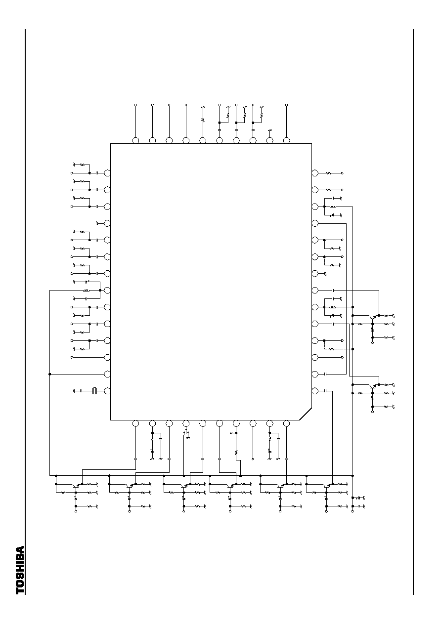
plication Circuit
YS1
B1-I
N
G1-IN
R1-IN
Y/C-G
ND
CR2-IN
CB2-I
N
Y2-I
N
Y/C-V
CC
B2-I
N
G2-IN
R2-IN
YS2/Y
M
FIL
X'tal
SDA
SCL
SYNC
-V
CC
YVI-
OU
T
SCP
HS
DIGI
TA
L-GND
DIGI
TA
L-V
DD
COMB
C-IN
/FOR
CE
D-S
VS
CVB
S-OU
T
SYNC
-IN
CVB
S1/
Y1-
IN
COMB
Y-I
N
CR-OUT
CB
-OUT
Y-
O
U
T
CLP
-
F
I
L
Y1
-
I
N
CB
1-I
N
CR1-I
N
SYN
C
-
G
N
D
YS3
C3-I
N
A
PC
-
F
IL
CV
B
S
3
/
Y
3
-
I
N
A
DDRE
S
S
C2-I
N
CV
B
S
2
/
Y
2
-
I
N
C
O
M
B
S
YS
FSC
-
OU
T
A
FC
-
F
IL
C1-I
N
39
40
41
42
43
44
45
46
47
48
1
2
3
4
5
7
6
8
9
10
11
12
13
14
24
23
22
21
20
19
18
17
16
15
38
37
36
35
34
32
33
31
30
29
28
27
26
25
0.1
m
F
75
W
B1-in
0.1
m
F
75
W
G1-in
0.1
m
F
75
W
R1-in
0.1
m
F
75
W
Cr2-in
0.1
m
F
75
W
0.1
m
F
75
W
0.1
m
F
75
W
Cb2-in
Y2-in
B2-in
0.1
m
F
75
W
G2-in
0.1
m
F
75
W
R2-in
YS2/Y
M
0.01
m
F
47
m
F
10 pF
16.2 M
Hz
YS1
Cr-out
Cb-out
Y
-
out
0.
1
m
F
75
W
Y1
-
i
n
0.
1
m
F
75
W
0.
1
m
F
75
W
Cb1-i
n
Cr1-i
n
YS3
4.
7
m
F
2.7 k
W
7.5 k
W
100
W
100
W
6.8 k
W
0.01
m
F
47
m
F
0.1
m
F
0.01
m
F
47
m
F
0.1
m
F
0.1
m
F
SDA
SCL
SCP
HS
VS
CVB
S-ou
t
0.
022
m
F
2.
2
m
F 3.
9
k
W
0.
01
m
F
0.
47
m
F 27
k
W
0.
01
m
F
0.
1
m
F
0.
01
m
F
0.
1
m
F
0.
01
m
F
10 k
W
C
o
m
b
S
YS
Fsc
-
out
8CH
8A
H
88H
A
dd S
W
A
B
1.5 k
W
6.8 k
W
75
W
16 k
W
10
m
F
1.8 k
W
10 k
W
75
W
10 k
W
10
m
F
1.5 k
W
6.8 k
W
75
W
16 k
W
10
m
F
1.8 k
W
10 k
W
75
W
10 k
W
10
m
F
1.5 k
W
6.8 k
W
75
W
16 k
W
10
m
F
1.8 k
W
10 k
W
75
W
10 k
W
10
m
F
C3-i
n
C
VBS3
/
Y3
-
i
n
C2-i
n
C
VBS2
/
Y2
-
i
n
C1-i
n
5 V
C
VBS1
/
Y1
-
i
n
47
m
F
0.01
m
F
1.5 k
W
6.8 k
W
75
W
16 k
W
10
m
F
Com
b
Y
-
i
n
1.8 k
W
10 k
W
75
W
10 k
W
10
m
F
Com
b
C-i
n
0.01
m
F
TB
1239B
F

TB1239BF
2002-02-12
25
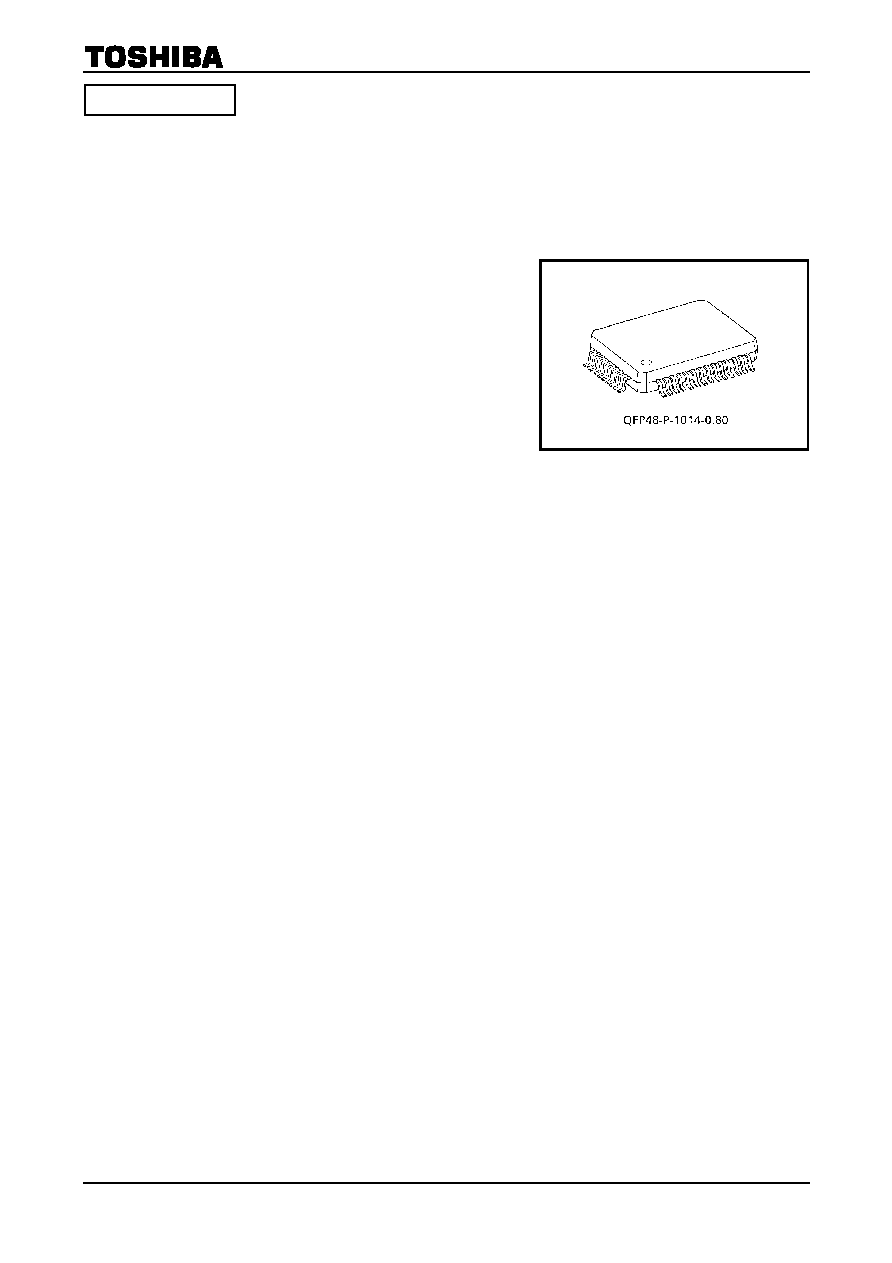
Package Dimensions
Weight: 0.83 g (typ.)

TB1239BF
2002-02-12
26
∑
TOSHIBA is continually working to improve the quality and reliability of its products. Nevertheless, semiconductor
devices in general can malfunction or fail due to their inherent electrical sensitivity and vulnerability to physical
stress. It is the responsibility of the buyer, when utilizing TOSHIBA products, to comply with the standards of
safety in making a safe design for the entire system, and to avoid situations in which a malfunction or failure of
such TOSHIBA products could cause loss of human life, bodily injury or damage to property.
In developing your designs, please ensure that TOSHIBA products are used within specified operating ranges as
set forth in the most recent TOSHIBA products specifications. Also, please keep in mind the precautions and
conditions set forth in the "Handling Guide for Semiconductor Devices," or "TOSHIBA Semiconductor Reliability
Handbook" etc..
∑
The TOSHIBA products listed in this document are intended for usage in general electronics applications
(computer, personal equipment, office equipment, measuring equipment, industrial robotics, domestic appliances,
etc.). These TOSHIBA products are neither intended nor warranted for usage in equipment that requires
extraordinarily high quality and/or reliability or a malfunction or failure of which may cause loss of human life or
bodily injury ("Unintended Usage"). Unintended Usage include atomic energy control instruments, airplane or
spaceship instruments, transportation instruments, traffic signal instruments, combustion control instruments,
medical instruments, all types of safety devices, etc.. Unintended Usage of TOSHIBA products listed in this
document shall be made at the customer's own risk.
∑
The products described in this document are subject to the foreign exchange and foreign trade laws.
∑
The information contained herein is presented only as a guide for the applications of our products. No
responsibility is assumed by TOSHIBA CORPORATION for any infringements of intellectual property or other
rights of the third parties which may result from its use. No license is granted by implication or otherwise under
any intellectual property or other rights of TOSHIBA CORPORATION or others.
∑
The information contained herein is subject to change without notice.
000707EBA
RESTRICTIONS ON PRODUCT USE