 | –≠–ª–µ–∫—Ç—Ä–æ–Ω–Ω—ã–π –∫–æ–º–ø–æ–Ω–µ–Ω—Ç: TB62206FG | –°–∫–∞—á–∞—Ç—å:  PDF PDF  ZIP ZIP |

TB62206FG
2005-03-02
1
TOSHIBA BiCD Processor IC Silicon Monolithic
TB62206FG
BiCD PWM 2-Phase Bipolar Stepping Motor Driver
The TB62206FG is designed to drive a 2-phase bipolar
setpping motor. With BiCD process technology, this device
enables output withstand voltage of 40 V and maximum current
of 1.8 A to be achieved.
Features
∑ Bipolar stepping motor driver IC
∑ Internal PWM current control
∑ 2-phase/1-2 phase excitation is available
∑ Monolithic BiCD IC
DMOS FET used for output power transistor
∑ High voltage output and High current: 40 V/1.8 A (max)
∑ On-chip thermal shutdown circuit, overcurrent protection circuit and power-on reset circuit (POR)
∑ Package: HSOP20-P-450-1.00
Pin Assignment
Weight: 0.79 g (typ.)
CR
V
DD
Vref A
Vref B
R
S
B
FIN (GND)
R
S
A
V
M
Ccp C
Ccp B
Ccp A
TORQUE
B
OUT
ENABLE B
ENABLE A
FIN (GND)
OUT A
PHASE B
PHASE A
STANDBY
11
10
20
1
A
OUT
OUT B
TB62206FG
2005-03-02
2
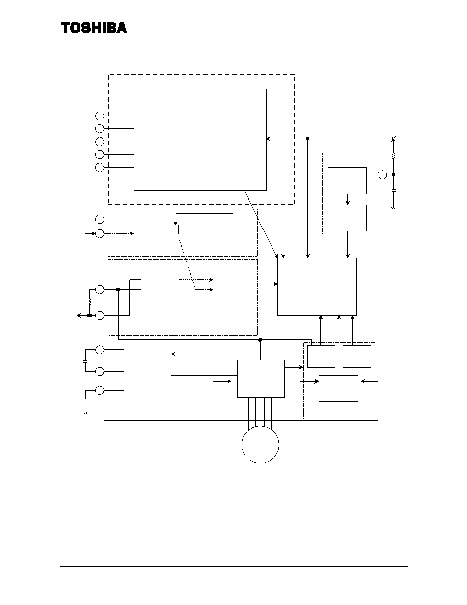
Block Diagram
STANDBY
ENABLE A
PHASE A
PHASE B
R
S
V
M
Ccp C
Ccp B
Ccp A
V
DD
Chopper OSC
Current Level Set
Current Feedback (
◊2)
Protection Unit
V
ref
ENABLE
V
M
V
DD
Stepping
motor
Input logic
Torque Control
V
RS
R
S COMP
Charge
Pump
Unit
Output
(H-Bridge)
◊2
OCS
CR-CLK
Converter
Output Control
(Mixed Decay Control)
TSD
ISD
V
DDR
/V
MR
Protect
CR
V
M
ENABLE B
TORQUE
STANDBY
TB62206FG
2005-03-02
3
Function Table
Output
Phase
Enable
OUT (+)
OUT ()
X L
OFF
OFF
H H H L
L H L H
X :
Don't care
Others
Pin Name
H
L
Notes
ENABLE X
Output
Output OFF
Output is OFF regardless of its phase's
state.
PHASE X
OUT X: H
X
OUT
: H
In high level, current flows OUT X
X
OUT
STANDBY
Motor operation enable
All functions of the
IC stopped
When
STANDBY
= L, output stopped while
charge pomp stopped.
TORQUE 100%
71%
High-level
Protection Function
(1) Thermal
shutdown
circuit
While Tj = 150∞C, all outputs are OFF. To turn-on, change the state of the STANDBY pin in the
order of H, L, H.
It has temperature hysteresis to prevent the output from oscillating. (T = 35∞C)
(2) POR (Power-On Reset Circuit: V
M
and V
DD
power supply monitor circuit)
Output is forcibly turned off until V
M
and V
DD
reach their specified levels.
(3) ISD
Output is forcibly turned off when current higher than the specified level flows in the output block.
To turn-on, change the state of the STANDBY pin in the order of H, L, H.

TB62206FG
2005-03-02
4
Timing Chart
(1) Full Step
(2) Half Step
H
L
H
L
H
L
100%
-100%
100%
-100%
PHASE A
PHASE B
ENABLE A
I
O
(A)
H
L
ENABLE B
I
O
(B)
H
L
H
L
H
L
100%
0%
-100%
100%
PHASE A
PHASE B
ENABLE A
I
O
(A)
H
L
ENABLE B
I
O
(B)
0%
-100%
TB62206FG
2005-03-02
5
Maximum Ratings
(Ta
=
25∞C)
Characteristics Symbol
Rating
Unit
Logic supply voltage
V
DD
7 V
Motor supply voltage
V
M
40
V
Output current
(Note 1)
I
OUT
1.8
A/phase
Current detect pin voltage
V
RS
V
M
± 4.5 V
V
Charge pump pin maximum voltage
(CCP1 pin)
V
H
V
M
+ 7.0
V
Logic input voltage
(Note 2)
V
IN
to
V
DD
+ 0.4
V
(Note 3)
1.4
Power dissipation
(Note 4)
P
D
3.2
W
Operating temperature
T
opr
-40 to 85
∞C
Storage temperature
T
stg
-55 to 150
∞C
Junction temperature
T
j
150
∞C
Note 1: Perform thermal calculations for the maximum current value under normal conditions. Use the IC at 1.5 A or
less per phase.
The current value maybe controled according to the ambient temperature or board conditions.
Note 2: Input 7 V or less as V
IN
Note 3: Measured for the IC only. (Ta
= 25∞C)
Note 4: Measured when mounted on the board. (Ta
= 25∞C)
Ta: IC ambient temperature
T
opr
: IC ambient temperature when starting operation
T
j
: IC chip temperature during operation T
j
(max) is controlled by TSD (thermal shut down circuit)
Recommended Operating Conditions
(Ta
=
0 to
85∞C, (Note 5))
Characteristics Symbol
Test
Condition
Min
Typ.
Max
Unit
Power supply voltage
V
DD
4.5
5.0
5.5
V
Motor supply voltage
V
M
V
DD
= 5.0 V, Ccp1 = 0.22 µF,
Ccp2
= 0.02 µF
13 24 35 V
Output current
I
OUT (1)
Ta
= 25∞C, per phase
1.2 1.5 A
Logic input voltage
V
IN
GND
V
DD
V
Phase signal input frequency
f
PHASE
V
DD
= 5.0 V
1.0 150 KHz
Chopping frequency
f
chop
V
DD
= 5.0 V
50
100
150
KHz
V
ref
reference voltage
V
ref
V
M
= 24 V, Torque = 100%
GND
3.0
4.0
V
Current detect pin voltage
V
RS
V
DD
= 5.0 V
0
±1.0
±4.5 V
Note 5: Because the maximum value of T
j
is 120∞C, recommended maximum current usage is below 120∞C.

TB62206FG
2005-03-02
6
Electrical Characteristics
1
(unless otherwise specified, Ta
=
25∞C, V
DD
=
5 V, V
M
=
24 V)
Characteristics Symbol
Test
Circuit
Test Condition
Min
Typ.
Max
Unit
HIGH V
IN (H)
2.0
V
DD
V
DD
+ 0.4
Input voltage
LOW V
IN (L)
DC
Data input pins
GND
- 0.4
GND 0.8
V
Input hysteresis voltage
V
IN (HIS)
DC
Data input pins
200
400
700
mV
I
IN (H)
Data input pins with resistor
35
50
75
I
IN (H)
1.0
Input current
I
IN (L)
DC
Data input pins without resistor
1.0
µA
I
DD1
V
DD
= 5 V, all inputs connected
to ground, Logic, output all off
1.0 2.0 3.0
Power dissipation (V
DD
pin)
I
DD2
DC
Output OPEN, f
PHASE
= 1.0 kHz
LOGIC ACTIVE, V
DD
= 5 V,
ChargePump
= charged
1.0 2.5 3.5
mA
I
M1
Output OPEN, all inputs
connected to ground, Logic,
output all off, ChargePump
=
no operation
1.0 2.0 3.0
I
M2
OUT OPEN, f
PHASE
= 1 kHz
LOGIC ACTIVE, V
DD
= 5 V,
V
M
= 24 V, Output off,
ChargePump
= charged
2.0 4.0 5.0
Power dissipation (V
M
pin)
I
M3
DC
OUT OPEN, f
PHASE
= 4 kHz
LOGIC ACTIVE, 100 kHz
chopping (emulation), Output
OPEN,
ChargePump
= charged
10 13
mA
Output standby current
Upper
DC
DC
V
RS
= V
M
= 24 V, V
OUT
= 0 V,
STANDBY
= H, PHASE = H
-200
-150
µA
Output bias current
Upper
I
OB
DC
V
OUT
= 0 V, STANDBY = H
-100
-50
µA
Output leakage current
Lower
I
OL
DC
V
RS
= V
M
= CcpA = V
OUT
= 24
V, LOGIC IN
= ALL = L
1.0 1.0 µA
HIGH
(reference)
V
RS (H)
V
ref
= 3.0 V, V
ref
(Gain)
= 1/5.0
TORQUE
= (H) = 100% set
100
Comparator reference
voltage ratio
LOW V
RS (L)
DC
V
ref
= 3.0 V, V
ref
(Gain)
= 1/5.0
TORQUE
= (L) = 71% set
66 71 76
%
Output current differential
I
OUT1
DC
Differences between output
current channels
-5
5 %
Output current setting differential
I
OUT2
DC
I
OUT
= 1000 mA
-5
5 %
RS pin current
I
RS
DC
V
RS
= 24 V, V
M
= 24 V
STANDBY
= L
1 2 µA
R
ON (D-S) 1
I
OUT
= 1.0 A, V
DD
= 5.0 V
T
j
= 25∞C, Drain-Source
0.5 0.6
R
ON (S-D) 1
I
OUT
= 1.0 A, V
DD
= 5.0 V
T
j
= 25∞C, Source-Drain
0.5 0.6
R
ON (D-S) 2
I
OUT
= 1.0 A, V
DD
= 5.0 V
T
j
= 105∞C, Drain-Source
0.6 0.75
Output transistor drain-source
ON-resistance
R
ON (S-D) 2
DC
I
OUT
= 1.0 A, V
DD
= 5.0 V
T
j
= 105∞C, Source-Drain
0.6 0.75
TB62206FG
2005-03-02
7
Electrical Characteristics
2
(unless otherwise specified, Ta
=
25∞C, V
DD
=
5 V, V
M
=
24 V)
Characteristics Symbol
Test
Circuit
Test Condition
Min
Typ.
Max
Unit
V
ref
input voltage
V
ref
DC
V
M
= 24 V, V
DD
= 5 V,
STANDBY
= H, Output on,
PHASE
= 1 kHz
GND
4.0 V
V
ref
input current
I
ref
DC
STANDBY
= H, Output on,
V
M
= 24 V, V
DD
= 5 V,
V
ref
= 3.0 V
20 35 50
µA
V
ref
attenuation ratio
V
ref
(GAIN)
DC
V
M
= 24 V, V
DD
= 5 V,
STANDBY
= H, Output on,
V
ref
= 0.0 to 4.0 V
1/4.8 1/5.0 1/5.2
TSD temperature
(Note 1)
T
j
TSD DC
V
DD
= 5 V, V
M
= 24 V
130
170 ∞C
TSD return temperature difference
(Note
1)
T
j
TSD DC
T
j
TSD
= 130 to 170∞C
T
j
TSD
- 50
T
j
TSD
- 35
T
j
TSD
- 20
∞C
V
DD
return voltage
V
DDR
DC
V
M
= 24 V, STANDBY =
H 2.0 3.0 4.0 V
V
M
return voltage
V
MR
DC
V
DD
= 5 V, STANDBY = H
8.0
9.0
10
V
Over current protected circuit
operation current
(Note 2)
ISD
V
DD
= 5 V, V
M
= 24 V
3.0 A
Note 1: Thermal shut down (TSD) circuit
When the IC junction temperature reaches the specified value and the TSD circuit is activated, the internal
reset circuit is activated switching the outputs of both motors to off.
When the temperature is set between 130 (min) to 170∞C (max), the TSD circuit operates.
When the TSD circuit is activated, the charge pump is halted, and TROTECT pin outputs V
DD
voltage.
Even if the TSD circuit is activated and STANDBY goes H L H instantaneously, the IC is not reset
until the IC junction temperature drops -20∞C (typ.) below the TSD operating temperature (hysteresis
function).
Note 2: Overcurrent protection circuit
When current exceeding the specified value flows to the output, the internal reset circuit is activated, and the
ISD turns off the output.
Until the STANDBY signal goes Low to High, the overcurrent protection circuit remains activated.
During ISD, IC turns STANDBY mode and the charge pump halts.
TB62206FG
2005-03-02
8
AC Electrical Characteristics
(Ta
=
25∞C, V
M
=
24 V, V
DD
=
5 V, 6.8 mH/5.7
)
Characteristics Symbol
Test
Circuit
Test Condition
Min
Typ.
Max
Unit
Clock frequency
f
PHASE
AC
166 kHz
t
w
(t
CLK
)
100
t
wp
50
Minimum clock pulse width
t
wn
AC
50
µs
t
r
Output Load: 6.8 mH/5.7
100
t
f
100
t
pLH
PHASE to OUT
1000
t
pHL
Output Load: 6.8 mH/5.7
2000
t
pLH
CR to OUT
500
Output transistor switching
characteristic
t
pHL
Output Load: 6.8 mH/5.7
1000
ns
Noise rejection dead band time
t
BRANK
I
OUT
= 1.0 A
200
300
500
ns
CR reference signal oscillation
frequency
f
CR
C
osc
= 560 pF, R
osc
= 3.6 k
800 kHz
Chopping frequency possible range
f
chop (min)
f
chop (max)
V
M
= 24 V, V
DD
= 5 V, Output
ACTIVE (I
OUT
= 1.0 A)
Step fixed, Ccp1
= 0.22 µF,
Ccp2
= 0.01 µF
40 100 150 kHz
Chopping set frequency
f
chop
Output ACTIVE (I
OUT
= 1.0 A),
CR CLK
= 800 kHz
100 kHz
Charge pump rise time
t
ONG
Ccp
= 0.22 µF, Ccp = 0.022 µF
V
M
= 24 V, V
DD
= 5 V,
STANDBY
= ON OFF
100 200 µs
TB62206FG
2005-03-02
9
Current Waveform and Setting of MIXED DECAY MODE
To control the constant current, the rate of Mixed Decay Mode which determines current amplitude
(ripple current) should be 37.5%.
MIXED DECAY MODE Waveform
(current waveform)
NF
f
chop
37.5%
MIXED
DECAY
MODE
CR pin
internal
CLK
waveform
Charge mode
NF: set current value reached Slow mode
Mixed decay timing Fast mode Charge mode
Set current value
MDT
DECAY MODE 1
NF
NF
25%
MIXED
DECAY
MODE
Internal
CR CLK
signal
I
OUT
f
chop
f
chop
Set current
value
Set current value
RNF
MDT (MIXED DECAY TIMING) point: 37.5% fixed

TB62206FG
2005-03-02
10
CLK Signal, Internal CR CLK, and Output Current Waveform
(when CLK signal is input in 2 excitation mode)
37.5 MIXED DECAY MODE
PHASE signal input
f
chop
Reset CR-CLK counter here
f
chop
f
chop
Set current
value
I
OUT
Set current value
NF
0
MDT
NF

TB62206FG
2005-03-02
11
Current Discharge Path when ENABLE Input During Operation
In Slow Mode, when all output transistors are forced to switch off, coil energy is discharged in the
following MODES:
Note: Parasitic diodes are located on dotted lines. In normal MIXED DECAY MODE, the current does not flow
to the parasitic diodes.
As shown in the figure above, an output transistor has parasitic diodes.
To discharge energy from the coil, each transistor is switched on allowing current to flow in the reverse
direction to that in normal operation. As a result, the parasitic diodes are not used. If all the output
transistors are forced to switch off, the energy of the coil is discharged via the parasitic diodes.
U1
L1
U2
L2
PGND
OFF
OFF
U1
L1
U2
L2
OFF
ON
(Note)
Load
PGND
U1
L1
U2
L2
OFF
OFF
(Note)
Load
PGND
(Note)
R
S
pin
R
RS
V
M
ON
ON
Load
Charge mode
Slow mode
Forced OFF mode
ON
R
S
pin
R
RS
V
M
R
S
pin
R
RS
V
M
OFF
OFF
Input ENABLE
OFF

TB62206FG
2005-03-02
12
Output Transistor Operating Mode
Output Transistor Operation Functions
CLK U1 U2 L1 L2
CHARGE
ON OFF OFF ON
SLOW OFF OFF ON ON
FAST OFF ON ON OFF
Note: The above table is an example where current flows in the direction of the arrows in the above figures.
When the current flows in the opposite direction of the arrows, see the table below.
CLK U1 U2 L1 L2
CHARGE
OFF ON ON OFF
SLOW OFF OFF ON ON
FAST ON OFF OFF ON
In this IC, three modes as shown above are automatically switched to control the constant current.
U1
L1
U2
L2
PGND
OFF
OFF
U1
L1
U2
L2
OFF
ON
ON
(Note)
Load
PGND
U1
L1
U2
L2
(Note)
Load
PGND
(Note)
R
S
pin
R
RS
V
M
ON
ON
Load
Charge mode
Current flows
into the coil.
Slow mode
Current flows between
the coil and the IC.
Fast mode
The energy in the coil flows
back to the power supply.
ON
R
S
pin
R
RS
V
M
R
S
pin
R
RS
V
M
OFF
OFF
ON
OFF

TB62206FG
2005-03-02
13
Power Supply Sequence
(recommended)
Note 1: If the V
DD
drops to the level of the V
DDR
or below while the specified voltage is input to the V
M
pin, the IC is
internally reset.
This is a protective measure against malfunction. Likewise, if the V
M
drops to the level of the V
MR
or below
while regulation voltage is input to the V
DD
, the IC is internally reset as a protective measure against
malfunction.
To avoid malfunction, when turning on V
M
or V
DD
, to input the STANDBY signal at the above timing is
recommended.
It takes time for the output control charge pump circuit to stabilize. Wait up to t
ONG
time after power on
before driving the motors.
Note 2: When the V
M
value is between 8 to 11 V, the internal reset is released, thus output may be on. In such a
case, the charge pump cannot drive stably because of insufficient voltage. The Standby state should be
maintained until V
M
reaches 13 V or more.
Note 3: Since V
DD
= 0 V and V
M
= voltage within the rating are applied, output is turned off by internal reset.
At that time, a current of several mA flows due to the Pass between V
M
and V
DD
.
When voltage increases on V
DD
output, make sure that specified voltage is input.
V
DD (max)
V
DD (min)
V
DDR
GND
V
DD
V
M
V
M (min)
V
MR
GND
V
M
Active
Non-active
Internal operable
H
L
STANDBY
INPUT (Note 1)
Takes up to t
ONG
until operable.
Non-operable area
STANDBY

TB62206FG
2005-03-02
14
How to Calculate Set Current
This IC drives the motor, controlling the PWM constant current in reference to the frequency of CR
oscillator.
At that time, the maximum current value (set current value) can be determined by setting the sensing
resistor (R
RS
) and reference voltage (V
ref
).
100(%)
x
)
(
RS
R
71%)
100,
(Torque
Torque
x
(V)
ref
V
x
5.0
1
(max)
OUT
I
=
=
1/5.0 is V
ref
(gain): V
ref
attenuation ratio. (for the specifications, see the electrical characteristics.)
For example, when applying V
ref
= 3 V and torque = 100% to drive out I
OUT
of 0.8 A, R
RS
= 0.75 (0.5 W
or more) is required.
(for 1-2 phase excitation with 71% of torque, the peak current should be set to 100%).
How to Calculate the Chopping and OSC Frequencies
At constant current control, this IC chops frequency using the oscillation waveform (saw tooth waveform)
determined by external capacitor and resistor as a reference.
The TB62206FG requires an oscillation frequency of eight times the chopping frequency.
The oscillation frequency is calculated as follows:
C)
600
R
(C
0.523
1
f
CR
◊
+
◊
◊
=
For example, when C
osc
= 560 pF and R
osc
= 3.6 k are connected, f
CR
= 813 kHz.
At this time, the chopping frequency f
chop
is calculated as follows:
f
chop
= f
CR
/8
= 101
kHz

TB62206FG
2005-03-02
15
IC Power Dissipation
IC power dissipation is classified into two: power consumed by transistors in the output block and power
consumed by the logic block and the charge pump circuit.
∑ Power consumed by the Power Transistor (calculated with R
ON
= 0.60 )
∑ In Charge mode, Fast Decay mode, or Slow Decay mode, power is consumed by the upper and lower
transistors of the H bridges.
The following expression expresses the power consumed by the transistors of a H bridge.
P (out) = 2 (T
r
) ◊ I
OUT
(A) ◊ V
DS
(V) = 2 ◊ I
OUT2
◊ R
ON
..............................(1)
The average power dissipation for output under 4-bit micro step operation (phase difference between
phases A and B is 90∞) is determined by expression (1).
Thus, power dissipation for output per unit is determined as follows (2) under the conditions below.
R
ON
= 0.60 (1.0 A)
I
OUT
(Peak: max) = 1.0 A
V
M
= 24 V
V
DD
= 5 V
P (out) = 2 (T
r
) ◊ 1.0
2
(A) ◊ 0.60 ◊ 2 () = 2.40 (W) ........................................(2)
Power consumed by the logic block and IM
The following standard values are used as power dissipation of the logic block and IM at operation.
I (LOGIC) = 2.5 mA (typ.):
I (I
M3
) = 10.0 mA (typ.): operation/unit
I (I
M1
) = 2.0 mA (typ.): stop/unit
The logic block is connected to V
DD
(5 V). IM (total of current consumed by the circuits connected to
V
M
and current consumed by output switching) is connected to V
M
(24 V). Power dissipation is
calculated as follows:
P (Logic&IM) = 5 (V) ◊ 0.0025 (A) + 24 (V) ◊ 0.010 (A) = 0.25 (W) ...............(3)
Thus, the total power dissipation (P) is
P = P (out) + P (Logic&IM) = 2.65 (W)
Power dissipation at standby is determined as follows:
P (standby) + P (out) = 24 (V) ◊ 0.002 (A) + 5 (V) ◊ 0.0025 (A) = 0.06 (W)
For thermal design on the board, evaluate by mounting the IC.

TB62206FG
2005-03-02
16
Test Waveforms
Phase
t phase
tpLH
tpHL
V
M
GND
t
r
t
f
10%
50%
90%
90%
50%
10%
Figure 1 Timing Waveforms and Names
TB62206FG
2005-03-02
17
OSC-Charge DELAY:
Because the rising edge level of the OSC waveform is used for converting the OSC waveform to the
internal CR CLK, a delay of up to 1.25 ns (@f
chop
= 100 kHz: f
CR
= 400 kHz) occurs between the OSC
waveform and the internal CR CLK.
CR Waveform
Internal CR CLK
Waveform
CR-CR CLK DELAY
Figure 2 Timing Waveforms and Names (CR and output)
t
chop
OSC-Charge Delay
H
L
Set current
OSC-Fast Delay
OSC (CR)
50%
50%
L
H
H
L
L
Charge
50%
Slow
Fast
OUTPUT
Voltage A
OUTPUT
Voltage A
OUTPUT
Current
TB62206FG
2005-03-02
18
P
D
≠ Ta
(package power dissipation)
(4) HSOP20
R
th (j-a)
only (96∞C/W)
(5) When mounted on the board (140 mm ◊ 70 mm ◊ 1.6 mm: 38∞C/W: typ.: under evaluation)
Note: R
th (j-a)
:
8.5∞C/W
Ambient temperature Ta (∞C)
P
D
≠ Ta
Po
wer
di
ssi
p
a
ti
on P
D
(
W
)
(2)
(1)
0
0
3.5
25 50 75 100
125
150
0.5
1
1.5
2
2.5
3

TB62206FG
2005-03-02
19
Relationship between V
M
and V
H
(charge pump voltage)
Note: V
DD
= 5 V
V
M
≠ V
H
(&Vcharge UP)
V
H
v
o
l
t
age
, c
har
ge
up
v
o
l
t
ag
e
(
V
)
Supply voltage VM (V)
Charge pump voltage VH = VDD + VM (= Ccp A) (V)
10
20
0
0
VH voltage
charge up voltage
VM voltage
2 3
10
20
30
40
4 5 6 7 8 9
11 12 13
14
15 16 17 18
21 22 23 24 25 26
19
27 28 29
31 32 33 34 35 36 37 38 39
1
30
40
50
Input
STANDBY
VMR
Charge pump
output voltage
VM voltage
Maximum rating
Recommended operation area
Usable area

TB62206FG
2005-03-02
20
Operation of Charge Pump Circuit
∑ Initial charging
(1) When RESET is released, T
r1
is turned ON and T
r2
turned OFF. Ccp 2 is charged from Ccp 2 via
Di1.
(2) T
r1
is turned OFF, T
r2
is turned ON, and Ccp 1 is charged from Ccp 2 via Di2.
(3) When the voltage difference between V
M
and V
H
(Ccp A pin voltage = charge pump voltage)
reaches V
DD
or higher, operation halts (steady state).
∑ Actual operation
(4) Ccp 1 charge is used at f
chop
switching and the V
H
potential drops.
(5) Charges up by (1) and (2) above.
Output switching
Initial charging
Steady state
(1)
(2) (3)
(4)
t
(5)
(4)
(5)
V
H
V
M
V
H
= V
M
+ V
DD
= charge pump voltage
i1 = charge pump output current
i2 = gate block power dissipation
V
DD
= 5 V
V
M
= 24 V
Comparator
&
Controller
V
M
Output
Output
H switch
i2
Ccp 1
0.22
µF
Ccp A
Ccp B
Ccp C
R
1
V
H
R
S
R
RS
Ccp 2
0.022
µF
Di2
Di1
Di3
V
z
i1
(2)
T
r1
T
r2
7
(1)
(2)
TB62206FG
2005-03-02
21
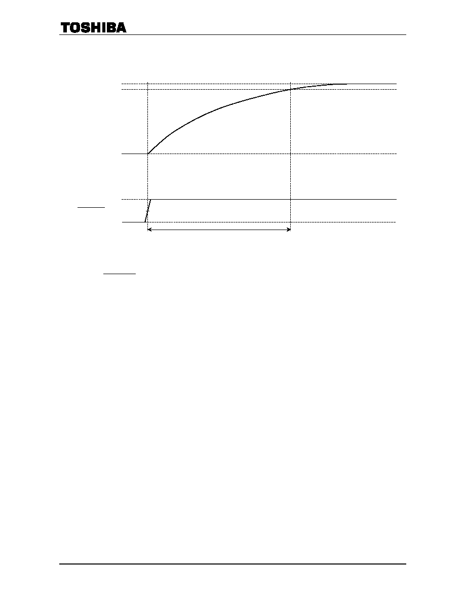
Charge Pump Rise Time
t
ONG
:
Delay time taken for capacitor Ccp 2 (charging capacitor) to fill up Ccp 1 (storing capacitor) to V
M
+ V
DD
after STANDBY is released.
The internal IC cannot drive the gates correctly until the voltage of Ccp 1 reaches V
M
+ V
DD
. Be sure to
wait for t
ONG
or longer before driving the motors.
Basically, the larger the Ccp 1 capacitance, the smaller the voltage fluctuation, though the initial charge
up time is longer.
The smaller the Ccp 1 capacitance, the shorter the initial charge-up time but the voltage fluctuation is
larger.
Depending on the combination of capacitors (especially with small capacitance), voltage may not be
sufficiently boosted.
When the voltage does not increase sufficiently, output DMOS R
ON
turns lower than the normal, and it
raises the temperature.
Thus, use the capacitors under the capacitor combination conditions (Ccp 1 = 0.22 µF, Ccp 2 = 0.022 µF)
recommended by Toshiba.
50%
V
DD
+ V
M
V
M
+ (V
DD
◊ 90%)
Ccp 1 voltage
V
M
5 V
0 V
STANDBY
t
ONG
TB62206FG
2005-03-02
22
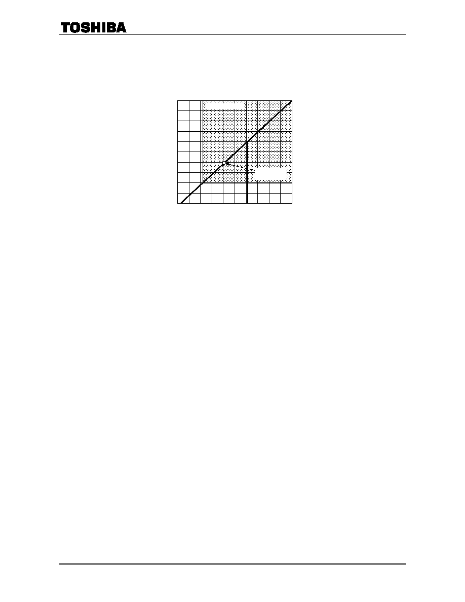
External Capacitor for Charge Pump
When driving the stepping motor with V
DD
= 5 V, f
chop
= 150 kHz, L
= 10 mH under the conditions of V
M
= 13 V and 1.5 A, the logical values for Ccp 1 and Ccp 2 are as shown in the graph below:
Choose Ccp 1 and Ccp 2 to be combined from the above applicable range. We recommend Ccp 1:Ccp 2 at
10:1 or more. (if our recommended values (Ccp
= 0.22 µF, Ccp 2
= 0.02 µF) are used, the drive conditions in
the specification sheet are satisfied. (there is no capacitor temperature characteristic as a condition.)
When setting the constants, make sure that the charge pump voltage is not below the specified value and
set the constants with a margin (the larger Ccp 1 and Ccp 2, the more the margin).
Some capacitors exhibit a large change in capacitance according to the temperature. Make sure the above
capacitance is obtained under the usage environment temperature.
Ccp 1 capacitance (µF)
Ccp 1 ≠ Ccp 2
Cc
p 2
ca
p
a
c
i
t
a
nce
(
µ
F)
0.05
0
0
0.005
0.01
0.015
0.02
0.025
0.03
0.035
0.04
0.045
0.05 0.1 0.15 0.2 0.25
0.35 0.4 0.45 0.5
0.3
Applicable range
Recommended
value
TB62206FG
2005-03-02
23
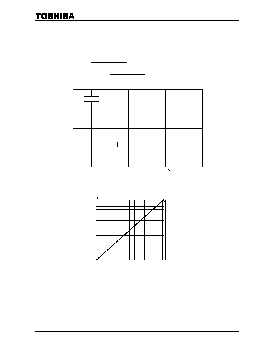
Driving Mode
2-Phase Excitation Mode
2-Phase Excitation
Note: 2-phase excitation has a large load change due to motor induced electromotive force. If a mode in
which the current attenuation capability (current control capability) is small is used, current increase
due to induced electromotive force may not be suppressed.
100
0
Phase B
Phase A
[%]
-100
STEP
Phase B
Phase A
0
100
IB (%)
2-Phase Excitation
IA
(%
)
100

TB62206FG
2005-03-02
24
1-2 Phase Excitation
Phase B
Phase A
100
0
[%]
-100
STEP
Phase B
Phase A
ENABLE B
ENABLE A
IB (%)
1-2 Phase Excitation (typ.A)
IA
(%
)
0
100
100

TB62206FG
2005-03-02
25
Recommended Application Circuit
The values for the respective devices are all recommended values. For values under each input condition,
see the above-mentioned recommended operating conditions.
Note: Adding bypass capacitors is recommended.
Make sure that GND wiring has only one contact point, and to design the pattern that allows the heat
radiation.
To control setting pins in each mode by SW, make sure to pull down or pull up them to avoid high
impedance.
To input the data, see the section on the recommended input data.
The IC may be destroyed due to short circuit between output pins, an output pin and the V
DD
pin, or an
output pin and the GND pin.
Design an output line, V
DD
(V
M
) line and GND line with great care.
Also a low-withstand-voltage device may be destroyed when mounted in the wrong orientation, which
causes high-withstanding voltage to be applied to the device.
M
R
osc
= 3.6 k
C
osc
= 560 pF
V
ref A
V
M
R
RS A
A
B
A
B
R
RS B
FIN
PHASE A
EANBLE B
ENABLE A
PHASE B
STANDBY
FIN
V
DD
CR
V
ref AB
3
V
1
µF
SGND
R
RS A
0.66
Stepping
motor
0.66
R
RS B
SGND
SGND
SGND
5 V
10
µF
Ccp C
Ccp B
Ccp A
Ccp 2
0.01
µF
Ccp 1
0.22
µF
TORQUE
0 V
24 V
SGND
100
µF
5 V
0 V
5 V
0 V
5 V
0 V
5 V
0 V
5 V
0 V
5 V
PGND
V
ref B
TB62206FG
2005-03-02
26
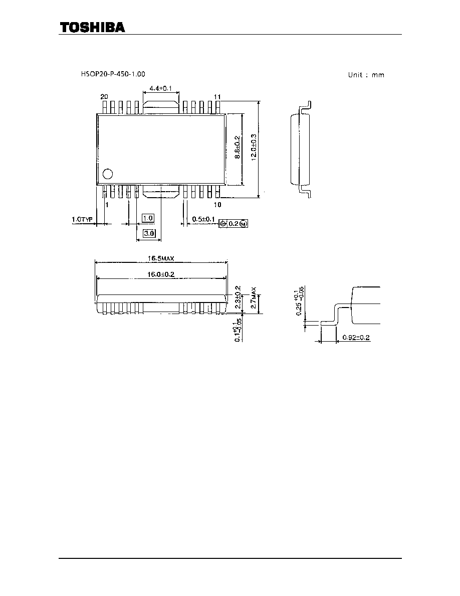
Package Dimensions
Weight: 0.79 g (typ.)

TB62206FG
2005-03-02
27
∑ The information contained herein is subject to change without notice.
∑ The information contained herein is presented only as a guide for the applications of our products. No
responsibility is assumed by TOSHIBA for any infringements of patents or other rights of the third parties which
may result from its use. No license is granted by implication or otherwise under any patent or patent rights of
TOSHIBA or others.
∑ TOSHIBA is continually working to improve the quality and reliability of its products. Nevertheless, semiconductor
devices in general can malfunction or fail due to their inherent electrical sensitivity and vulnerability to physical
stress. It is the responsibility of the buyer, when utilizing TOSHIBA products, to comply with the standards of
safety in making a safe design for the entire system, and to avoid situations in which a malfunction or failure of
such TOSHIBA products could cause loss of human life, bodily injury or damage to property.
In developing your designs, please ensure that TOSHIBA products are used within specified operating ranges as
set forth in the most recent TOSHIBA products specifications. Also, please keep in mind the precautions and
conditions set forth in the "Handling Guide for Semiconductor Devices," or "TOSHIBA Semiconductor Reliability
Handbook" etc..
∑ The TOSHIBA products listed in this document are intended for usage in general electronics applications
(computer, personal equipment, office equipment, measuring equipment, industrial robotics, domestic appliances,
etc.). These TOSHIBA products are neither intended nor warranted for usage in equipment that requires
extraordinarily high quality and/or reliability or a malfunction or failure of which may cause loss of human life or
bodily injury ("Unintended Usage"). Unintended Usage include atomic energy control instruments, airplane or
spaceship instruments, transportation instruments, traffic signal instruments, combustion control instruments,
medical instruments, all types of safety devices, etc.. Unintended Usage of TOSHIBA products listed in this
document shall be made at the customer's own risk.
∑ The products described in this document are subject to the foreign exchange and foreign trade laws.
∑ TOSHIBA products should not be embedded to the downstream products which are prohibited to be produced
and sold, under any law and regulations.
030619EBA
RESTRICTIONS ON PRODUCT USE