
TC58DVM72A1FT00/ TC58DVM72F1FT00
TC58DAM72A1FT00/ TC58DAM72F1FT00
2003-01-24 1/34
TENTATIVE
TOSHIBA MOS DIGITAL INTEGRATED CIRCUIT SILICON GATE CMOS
128-MBIT (16M 8 BITS/8M x 16BITS) CMOS NAND E
2
PROM
DESCRIPTION
The TC58DxM72x1xxxx is a 128-Mbit (138,412,032) bit NAND Electrically Erasable and Programmable
Read-Only Memory (NAND E
2
PROM) organized as 528 bytes/264 words 32 pages 1024 blocks. The device uses
dual power supplies (2.7 V to 3.6 V for V
CC
and 1.65 V to 1.95 V for V
CCQ
). The device has a 528-byte/264-words
static register which allows program and read data to be transferred between the register and the memory cell array
in 528-byte/256-words increments. The Erase operation is implemented in a single block unit (16 Kbytes 512 bytes:
528 bytes 32 pages/8k words + 256 words:264 words x 32 pages).
The TC58DxM72x1xxxx is a serial-type memory device which utilizes the I/O pins for both address and data
input/output as well as for command inputs. The Erase and Program operations are automatically executed making
the device most suitable for applications such as solid-state file storage, voice recording, image file memory for still
cameras and other systems which require high-density non-volatile memory data storage.
FEATURES
Organization TC58DxM72A1xxxx
TC58DxM72F1xxxx
Memory cell allay 528 32K 8
264 x 32k x 16
Register 528
8
264 x 16
Page size
528 bytes
264 words
Block size
(16K 512) bytes
(8k + 256) words
Modes
Read, Reset, Auto Page Program
Auto Block Erase, Status Read
Mode control
Serial input/output
Command control
Power supply
TC58DVM72x1xxxx TC58DAM72x1xxxx
Vcc: 2.7V to 3.6V 2.7V to 3.6V
Vccq: 2.7V to 3.6V 1.65V to 1.95V
Program/Erase Cycles 1E5 cycle (with ECC)
Access time
Cell array to register 25 s max
Serial Read Cycle
50 ns min
Operating current
Read (50 ns cycle) 10 mA typ.
Program (avg.)
10 mA typ.
Erase (avg.)
10 mA typ.
Standby 50
A max.
Package
TSOP I 48-P-1220-0.50 (Weight:0.53g typ)
TOSHIBA is continually working to improve the quality and reliability of its products. Nevertheless, semiconductor devices in general
can malfunction or fail due to their inherent electrical sensitivity and vulnerability to physical stress. It is the responsibility of the buyer,
when utilizing TOSHIBA products, to comply with the standards of safety in making a safe design for the entire system, and to avoid
situations in which a malfunction or failure of such TOSHIBA products could cause loss of human life, bodily injury or damage to
property.
In developing your designs, please ensure that TOSHIBA products are used within specified operating ranges as set forth in the most
recent TOSHIBA products specifications. Also, please keep in mind the precautions and conditions set forth in the "Handling Guide
for Semiconductor Devices," or "TOSHIBA Semiconductor Reliability Handbook" etc..
The TOSHIBA products listed in this document are intended for usage in general electronics applications (computer, personal
equipment, office equipment, measuring equipment, industrial robotics, domestic appliances, etc.). These TOSHIBA products are
neither intended nor warranted for usage in equipment that requires extraordinarily high quality and/or reliability or a malfunction or
failure of which may cause loss of human life or bodily injury ("Unintended Usage"). Unintended Usage include atomic energy control
instruments, airplane or spaceship instruments, transportation instruments, traffic signal instruments, combustion control
instruments, medical instruments, all types of safety devices, etc.. Unintended Usage of TOSHIBA products listed in this document
shall be made at the customer's own risk.
The products described in this document are subject to the foreign exchange and foreign trade laws.
The information contained herein is presented only as a guide for the applications of our products. No responsibility is assumed by
TOSHIBA CORPORATION for any infringements of intellectual property or other rights of the third parties which may result from its
use. No license is granted by implication or otherwise under any intellectual property or other rights of TOSHIBA CORPORATION or
others.
The information contained herein is subject to change without notice.
000707EBA1
TC58DVM72A1FT00/ TC58DVM72F1FT00
TC58DAM72A1FT00/ TC58DAM72F1FT00
2003-01-24 2/34
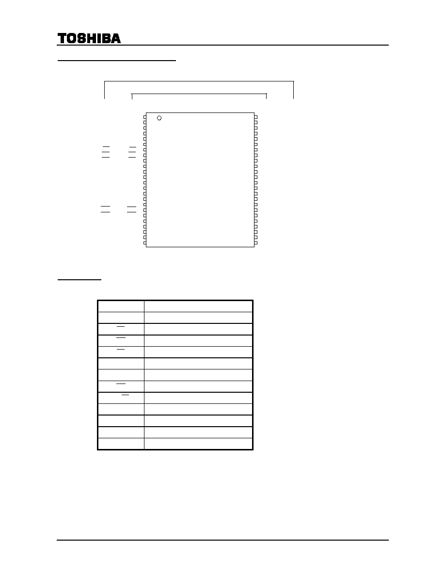
PIN ASSIGNMENT (TOP VIEW)
PINNAMES
I/O1 to I/O8
I/O port
I/O9 to I/O16
I/O port (x16)
CE Chip
enable
WE Write
enable
RE Read
enable
CLE Command
latch
enable
ALE
Address latch enable
WP Write
protect
BY
/
RY
Ready/Busy
GND
Ground input
V
CC
Power
supply
V
CCQ
I/O port Power supply
V
SS
Ground
TC58DVM72A1FT00 / TC58DAM72A1FT00
x8
NC
NC
NC
NC
I/O8
I/O7
I/O6
I/O5
NC
NC
NC
V
CCQ
V
SS
NC
NC
NC
I/O4
I/O3
I/O2
I/O1
NC
NC
NC
NC
1 48
2 47
3 46
4 45
5 44
6 43
7 42
8 41
9 40
10 39
11 38
12 37
13 36
14 35
15 34
16 33
17 32
18 31
19 30
20 29
21 28
22 27
23 26
24 25
x8
NC
NC
NC
NC
NC
GND
BY
/
RY
RE
CE
NC
NC
V
CC
V
SS
NC
NC
CLE
ALE
WE
WP
NC
NC
NC
NC
NC
x16
NC
NC
NC
NC
NC
GND
BY
/
RY
RE
CE
NC
NC
V
CC
V
SS
NC
NC
CLE
ALE
WE
WP
NC
NC
NC
NC
NC
TC58DVM72F1FT00 / TC58DAM72F1FT00
x16
V
SS
I/O16
I/O8
I/O15
I/O7
I/O14
I/O6
I/O13
I/O5
NC
NC
V
CCQ
NC
NC
NC
I/O12
I/O4
I/O11
I/O3
I/O10
I/O2
I/O9
I/O1
V
SS

TC58DVM72A1FT00/ TC58DVM72F1FT00
TC58DAM72A1FT00/ TC58DAM72F1FT00
2003-01-24 3/34
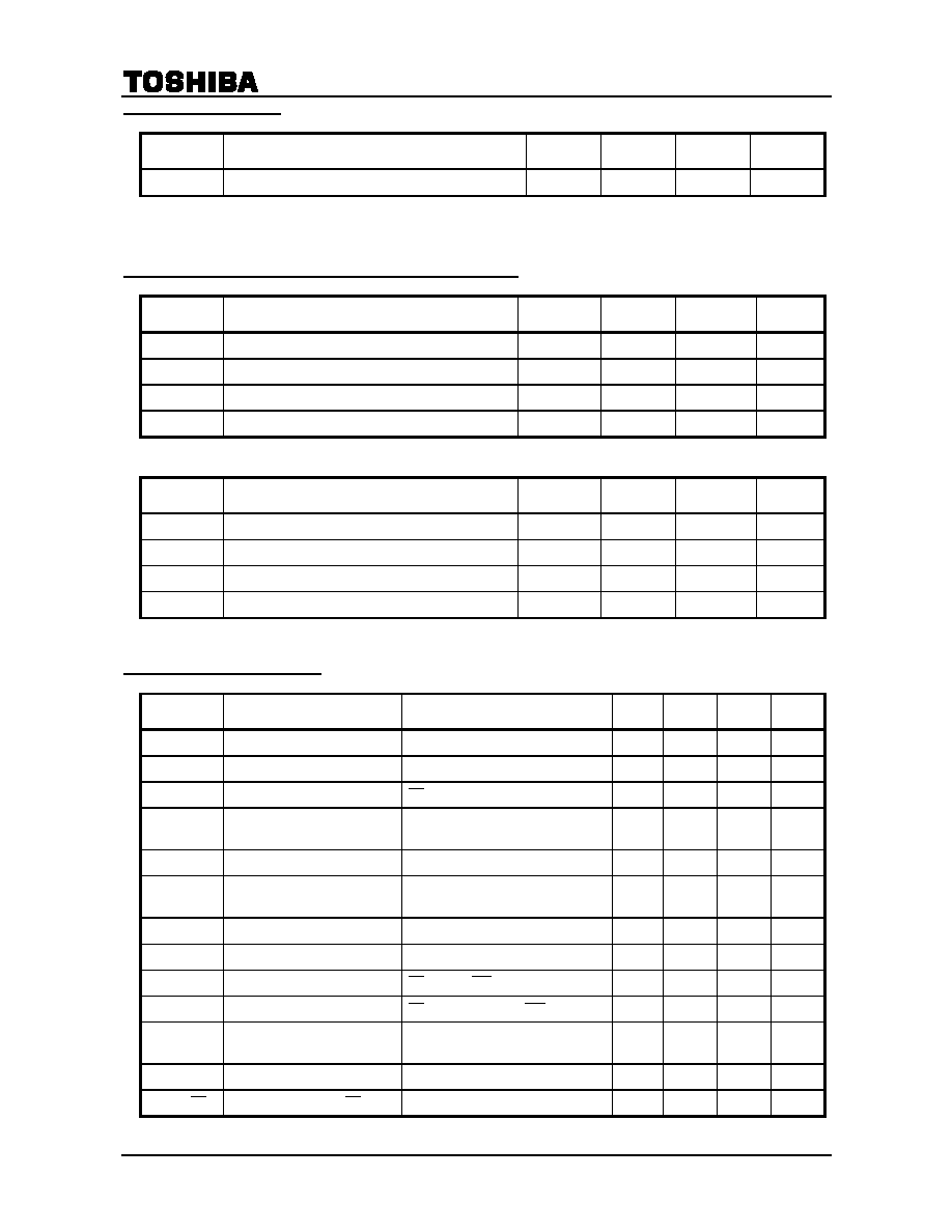
BLOCK DIAGRAM
ABSOLUTE MAXIMUM RATINGS
VALUE
SYMBOL RATING
TC58DVxxxxx TC58DAxxxx
unit
V
CC
Power Supply Voltage
0.6~4.6
0.6~4.6 V
V
CCQ
I/O port Power Supply Voltage
0.6~4.6
0.6~2.6 V
V
IN
Input Voltage for Control pins
0.6~4.6
0.6~2.6 V
V
I/O
Input/Output Voltage for I/O pins
0.6 V~V
CCQ
0.3 V (
4.6 V)
0.6 V~V
CCQ
0.3 V (
2.6 V)
P
D
Power Dissipation
0.3
0.3
W
T
solder
Soldering
Temperature(10s)
260
260
�C
T
stg
Storage Temperature
55~150
55~150 �C
T
opr
Operating Temperature
0~70
0~70
�C
CAPACITANCE *(Ta =25�C, f= 1 MHz)
SYMB0L PARAMETER
CONDITION
MIN
MAX
UNIT
C
IN
Input
V
IN
0 V
10 pF
C
OUT
Output
V
OUT
0 V
10 pF
* This parameter is periodically sampled and is not tested for every device.
V
CC
I/O Control circuit
Status register
Address register
Command register
Column buffer
Column decoder
Data register
Sense amp
Memory cell array
Control
HV generator
Row add
ress decoder
Logic control
BY
/
RY
I/O1
V
SS
I/O8
or
I/O16
to
WP
CE
CLE
ALE
WE
RE
BY
/
RY
Row add
ress buf
fer
decoder
V
CCQ
TC58DVM72A1FT00/ TC58DVM72F1FT00
TC58DAM72A1FT00/ TC58DAM72F1FT00
2003-01-24 4/34
VALID BLOCKS (1)
SYMBOL PARAMETER MIN
TYP.
MAX
UNIT
N
VB
Number of Valid Blocks
1004
1024 Blocks
(1) The device occasionally contains unusable blocks. Refer to Application Note (13) toward the end of this document.
(2) The first block (block address #00) is guaranteed to be a valid block at the time of shipment.
RECOMMENDED DC OPERATING CONDITIONS
TC58DVM72A1xxxx,TC58DVM72F1xxxx
SYMBOL PARAMETER
MIN
TYP.
MAX
UNIT
V
CC
Power Supply Voltage
2.7
3.3
3.6
V
V
CCQ
I/O Port Power Supply Voltage
2.7
3.6 V
V
IH
High Level input Voltage
2.0
V
CCQ
0.3
V
V
IL
Low Level Input Voltage
0.3
*
0.8 V
*
2 V (pulse width lower than 20 ns)
TC58DAM72A1xxxx,TC58DAM72F1xxxx
SYMBOL PARAMETER
MIN
TYP.
MAX
UNIT
V
CC
Power Supply Voltage
2.7
3.3
3.6
V
V
CCQ
I/O Port Power Supply Voltage
1.65
1.8
1.95 V
V
IH
High Level input Voltage
V
CCQ
X 0.78
V
CCQ
0.3
V
V
IL
Low Level Input Voltage
0.3
*
V
CCQ
X 0.22
V
*
2 V (pulse width lower than 20 ns)
DC CHARACTERISTICS (Ta = 0� to 70�C, V
CC
2.7 V to 3.6 V)
SYMBOL PARAMETER
CONDITION
MIN
TYP.
MAX
UNIT
I
IL
Input Leakage Current
V
IN
0 V to V
CCQ
10
A
I
LO
Output
Leakage
Current
V
OUT
0 V to V
CCQ
10
A
I
CCO1
Operating Current (Serial Read)
CE V
IL
, I
OUT
0 mA, t
cycle
50 ns
10 30 mA
I
CCO3
Operating Current
(Command Input)
t
cycle
50 ns
10 30 mA
I
CCO4
Operating Current (Data Input)
t
cycle
50 ns
10 30 mA
I
CCO5
Operating Current
(Address Input)
t
cycle
50 ns
10 30 mA
I
CCO7
Programming
Current
10 30 mA
I
CCO8
Erasing
Current
10 30 mA
I
CCS1
Standby
Current
CE V
IH,
WP 0 V/V
CCQ
1 mA
I
CCS2
Standby
Current
CE V
CCQ
0.2 V, WP 0 V/V
CCQ
10 50 A
V
OH
High Level Output Voltage
I
OH
mA
V
CCQ
-0.5
V
V
OL
Low Level Output Voltage
I
OL
2.1 mA
0.4 V
I
OL
(
BY
/
RY
) Output
Current
of
BY
/
RY
pin
V
OL
0.4 V
8
mA

TC58DVM72A1FT00/ TC58DVM72F1FT00
TC58DAM72A1FT00/ TC58DAM72F1FT00
2003-01-24 5/34
AC CHARACTERISTICS AND RECOMMENDED OPERATING CONDITIONS
(Ta 0� to 70�C, V
CC
2.7 V to 3.6 V)
SYMBOL PARAMETER
MIN
MAX
UNIT
NOTES
tCLS CLE
Setup
Time
0
ns
tCLH CLE
Hold
Time
10
ns
tCS
CE
Setup Time
0
ns
tCH
CE
Hold Time
10
ns
tWP Write
Pulse
Width
25
ns
tALS ALE
Setup
Time
0
ns
tALH ALE
Hold
Time
10
ns
tDS Data
Setup
Time
20
ns
tDH Data
Hold
Time
10
ns
tWC Write
Cycle
Time
50
ns
tWH
WE
High Hold Time
15
ns
tWW
WP
High to WE Low
100
ns
tRR Ready
to
RE
Falling Edge
20
ns
tRP Read
Pulse
Width
35
ns
tRC Read
Cycle
Time
50
ns
tREA
RE
Access Time (Serial Data Access)
35 ns
tCEA
CE
Access Time (Serial Data Access,ID Read)
45 ns
tALEA
ALE Access Time (ID Read)
ns
tCEH
CE
High Time for Last Address in Serial Read Cycle
Ns
(2)
tREAID
RE
Access Time (ID Read)
35 ns
tOH
Data Output Hold Time
10
ns
tRHZ
RE
High to Output High Impedance
30 ns
tCHZ
CE
High to Output High Impedance
20 ns
tREH
RE
High Hold Time
15
ns
tIR Output-High-impedance-to- RE Falling Edge
0
ns
tRSTO
RE
Access Time (Status Read)
35 ns
tCSTO
CE
Access Time (Status Read)
45 ns
tRHW
RE
High to WE Low
0
ns
tWHC
WE
High to CE Low
30
ns
tWHR
WE
High to RE Low
30
ns
tR
Memory Cell Array to Starting Address
25 s
tWB
WE
High to Busy
200 ns
tAR2
ALE Low to RE Low (Read Cycle)
50
ns
tRB
RE
Last Clock Rising Edge to Busy(in Sequential Read)
200 ns
tCRY
CE
High to Ready(When interrupted by CE in Read Mode)
1+
tr(
BY
/
RY
)
s
(1)(2)
tRST Device
Reset
Time
(Read/Program/Erase)
6/10/500 s
AC TEST CONDITIONS
CONDITION
PARAMETER
TC58DVxxxxx TC58DAxxxx
Input level
2.4 V, 0.4 V
V
CCQ
-0.2 V, 0.2 V
Input pulse rise and fall time
3 ns
3 ns
Input comparison level
1.5 V, 1.5 V
0.9 V, 0.9 V
Output data comparison level
1.5 V, 1.5 V
0.9 V, 0.9 V
Output load
C
L
(100 pF) 1 TTL
C
L
(30 pF)