TC58NVG0S3AFT05
2003-08-20A 1/33
TENTATIVE TOSHIBA MOS DIGITAL INTEGRATED CIRCUIT SILICON GATE CMOS
1 GBIT (128M
◊
8 BITS) CMOS NAND EEPROM
DESCRIPTION
The TC58NVG0S3A is a single 3.3-V 1G-bit (1,107,296,256 bits) NAND Electrically Erasable and Programmable
Read-Only Memory (NAND EEPROM) organized as (2048
+ 64) bytes ◊ 64 pages ◊ 1024 blocks. The device has a
2112-byte static registers which allow program and read data to be transferred between the register and the
memory cell array in 2112-byte increments. The Erase operation is implemented in a single block unit (128 Kbytes
+ 4 Kbytes: 2112 bytes ◊ 64 pages).
The TC58NVG0S3A is a serial-type memory device which utilizes the I/O pins for both address and data
input/output as well as for command inputs. The Erase and Program operations are automatically executed
making the device most suitable for applications such as solid-state file storage, voice recording, image file
memory for still cameras and other systems which require high-density non-volatile memory data storage.
FEATURES
∑ Organization
Memory cell array 2112
◊ 64K ◊ 8
Register 2112
◊ 8
Page size
2112 bytes
Block size
(128K
+ 4K) bytes
∑ Modes
Read, Reset, Auto Page Program
Auto Block Erase, Status Read
∑ Mode control
Serial input/output
Command control
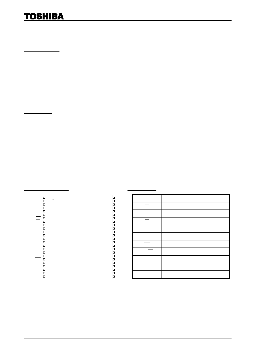
PIN ASSIGNMENT
(TOP VIEW)
PIN
NAMES
I/O1 to I/O8
I/O port
CE
Chip
enable
WE Write
enable
RE Read
enable
CLE
Command latch enable
ALE Address
latch
enable
WP Write
protect
BY
/
RY
Ready/Busy
GND Ground
Input
V
CC
Power
supply
V
SS
Ground
∑ Powersupply V
CC
= 2.7 V to 3.6 V
∑ Program/Erase Cycles
1E5 Cycles (With ECC)
∑ Access time
Cell array to register
25
µs max
Serial Read Cycle
50 ns min
∑ Operating current
Read (50 ns cycle)
10 mA typ.
Program (avg.)
10 mA typ.
Erase (avg.)
10 mA typ.
Standby 50
µA max
∑ Package
TSOPI48-P-1220-0.50 (Weight: 0.53 g typ.)
1 48
2 47
3 46
4 45
5 44
6 43
7 42
8 41
9 40
10 39
11 38
12 37
13 36
14 35
15 34
16 33
17 32
18 31
19 30
20 29
21 28
22 27
23 26
24 25
NC
NC
NC
NC
I/O8
I/O7
I/O6
I/O5
NC
NC
NC
V
CC
V
SS
NC
NC
NC
I/O4
I/O3
I/O2
I/O1
NC
NC
NC
NC
NC
NC
NC
NC
NC
GND
BY
/
RY
RE
CE
NC
NC
V
CC
V
SS
NC
NC
CLE
ALE
WE
WP
NC
NC
NC
NC
NC
TC58NVG0S3AFT05
2003-08-20A 2/33
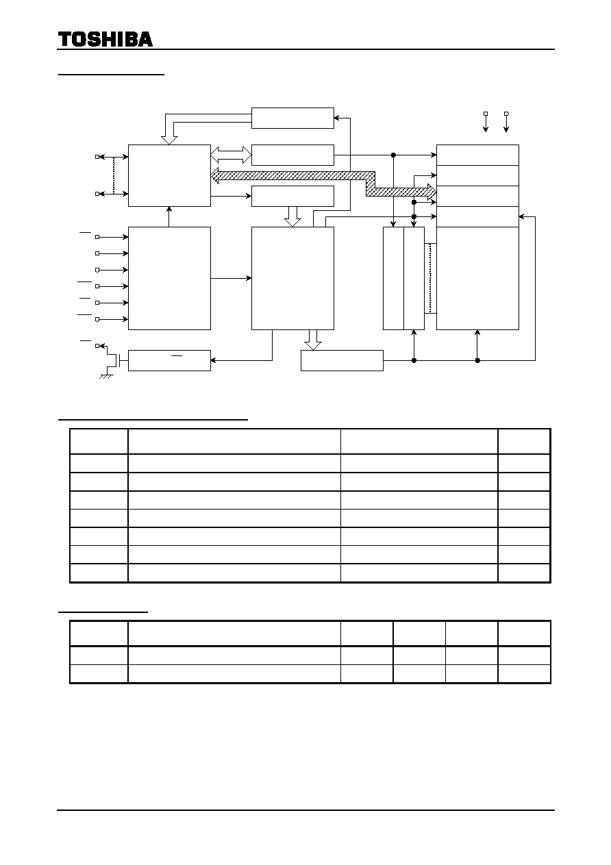
BLOCK DIAGRAM
ABSOLUTE MAXIMUM RATINGS
SYMBOL RATING
VALUE
UNIT
V
CC
Power Supply Voltage
-
0.6 to 4.6
V
V
IN
Input Voltage
-
0.6 to 4.6
V
V
I/O
Input /Output Voltage
-
0.6 V to V
CC
+
0.3 V (
4.6 V)
V
P
D
Power Dissipation
0.3
W
T
SOLDER
Soldering Temperature (10 s)
260
∞C
T
STG
Storage Temperature
-
55 to 150
∞C
T
OPR
Operating Temperature
0 to 70
∞C
CAPACITANCE
*
(Ta
=
=
=
=
25∞C, f
=
=
=
=
1 MHz)
SYMB0L PARAMETER
CONDITION
MIN
MAX
UNIT
C
IN
Input
V
IN
=
0 V
10 pF
C
OUT
Output
V
OUT
=
0 V
10 pF
*
This parameter is periodically sampled and is not tested for every device.
I/O
Control
circuit
Status register
Address register
Command register
Column buffer
Column decoder
Data register
Sense amp
Memory
cell array
Control
circuit
HV generator
Row
addres
s
dec
order
Logic
control
BY
/
RY
V
CC
I/O1
V
SS
I/O8
to
WP
CE
CLE
ALE
WE
RE
BY
/
RY
Row
addres
s
buf
f
e
r
dec
oder

TC58NVG0S3AFT05
2003-08-20A 3/33
VALID BLOCKS
(1)
SYMBOL PARAMETER MIN
TYP.
MAX
UNIT
N
VB
Number of Valid Blocks
1004
1024
Blocks
(1) The TC58NVG0S3A occasionally contains unusable blocks. Refer to Application Note (13) toward the end of this document.
(2) The first block (block address #00) is guaranteed to be a valid block at the time of shipment.
RECOMMENDED DC OPERATING CONDITIONS
SYMBOL PARAMETER MIN
TYP.
MAX
UNIT
V
CC
Power
Supply
Voltage
2.7 3.3 3.6 V
V
IH
High
Level
input
Voltage
2.0
V
CC
+
0.3
V
V
IL
Low Level Input Voltage
-
0.3
*
0.8 V
*
-
2 V (pulse width lower than 20 ns)
DC CHARACTERISTICS
(Ta
=
=
=
=
0 to 70∞C, V
CC
=
=
=
=
2.7 V~3.3 V)
SYMBOL PARAMETER
CONDITION
MIN
TYP.
MAX
UNIT
I
IL
Input
Leakage
Current
V
IN
=
0 V to V
CC
±
10
µ
A
I
LO
Output Leakage Current
V
OUT
=
0 V to V
CC
±
10
µ
A
I
CCO1
Reading
CE
=
V
IL
, I
OUT
=
0 mA, t
cycle
=
50 ns
10 30 mA
I
CCO2
Programming
Current
10 30 mA
I
CCO3
Erasing
Current
10 30 mA
I
CCS1
Standby
Current
CE
=
V
IH,
WP
=
0 V/V
CC
1 mA
I
CCS2
Standby
Current
CE
=
V
CC
-
0.2 V, WP
=
0 V/V
CC
50
µ
A
V
OH
High Level Output Voltage
V
CC
, I
OH
=
-
400
µ
A 2.4
V
V
OL
Low Level Output Voltage
V
CC
, I
OL
=
2.1 mA
0.4 V
I
OL
(
BY
/
RY
) Output
current
of
BY
/
RY
pin V
OL
=
0.4 V
8
mA

TC58NVG0S3AFT05
2003-08-20A 4/33
AC CHARACTERISTICS AND RECOMMENDED OPERATING CONDITIONS
(Ta
=
=
=
=
0 to 70∞C, V
CC
=
=
=
=
2.7 V~3.6 V)
SYMBOL PARAMETER
MIN
MAX
UNIT
NOTES
t
CLS
CLE
Setup
Time
0
ns
t
CLH
CLE
Hold
Time
10
ns
t
CS
CE
Setup Time
0
ns
t
CH
CE
Hold Time
10
ns
t
WP
Write
Pulse
Width
25
ns
t
ALS
ALE
Setup
Time
0
ns
t
ALH
ALE
Hold
Time
10
ns
t
DS
Data
Setup
Time
20
ns
t
DH
Data
Hold
Time
10
ns
t
WC
Write
Cycle
Time
50
ns
t
WH
WE High Hold Time
15
ns
t
WW
WP High to WE Low
100
ns
t
RR
Ready
to
RE Falling Edge
20
ns
t
RW
Ready
to
WE Falling Edge
20
ns
t
RP
Read
Pulse
Width
35
ns
t
RC
Read
Cycle
Time
50
ns
t
REA
RE Access Time (Serial Data Access)
35 ns
t
CEA
CE
Access Time
45 ns
t
CLEA
CLE
Access
Time
45 ns
t
ALEA
ALE Access Time
45 ns
t
REAID
RE Access Time (ID Read)
35 ns
t
OH
Data
Output
Hold
Time
10
ns
t
RHZ
RE High to Output High Impedance
30 ns
t
CHZ
CE
High to Output High Impedance
20 ns
t
REH
RE High Hold Time
15
ns
t
IR
Output-High-impedance-to- RE Falling Edge
0
ns
t
RSTO
RE Access Time (Status Read)
35 ns
t
CSTO
CE
Access Time (Status Read)
45 ns
t
CLSTO
CLE Access Time (Status Read)
45 ns
t
RHW
RE High to WE Low
30
ns
t
WHC
WE High to
CE
Low
30
ns
t
WHR
WE High to RE Low
30
ns
t
CR
CE
Low to RE Low (ID Read)
100
ns
t
R
Memory Cell Array to Starting Address
25
µ
s
t
WB
WE High to Busy
200 ns
t
RST
Device
Reset
Time
(Read/Program/Erase)
6/10/500
µ
s
TC58NVG0S3AFT05
2003-08-20A 5/33
AC TEST CONDITIONS
PARAMETER CONDITION
Input level
2.4 V, 0.4 V
Input pulse rise and fall time
3 ns
Input comparison level
1.5 V, 1.5 V
Output data comparison level
1.5 V, 1.5 V
Output load
C
L
(100 pF)
+
1 TTL
PROGRAMMING AND ERASING CHARACTERISTICS
(Ta
=
=
=
=
0 to 70∞C, V
CC
=
=
=
=
2.7 V~3.6 V)
SYMBOL PARAMETER MIN
TYP.
MAX
UNIT
NOTES
t
PROG
Average Programming Time
200 700
µ
s
N
Number of Programming Cycles on Same Page
(per 512
+
16 bytes)
2 (1)
t
BERASE
Block
Erasing
Time
2 4 ms
(1) Refer to Application Note (12) toward the end of this document.

TC58NVG0S3AFT05
2003-08-20A 6/33
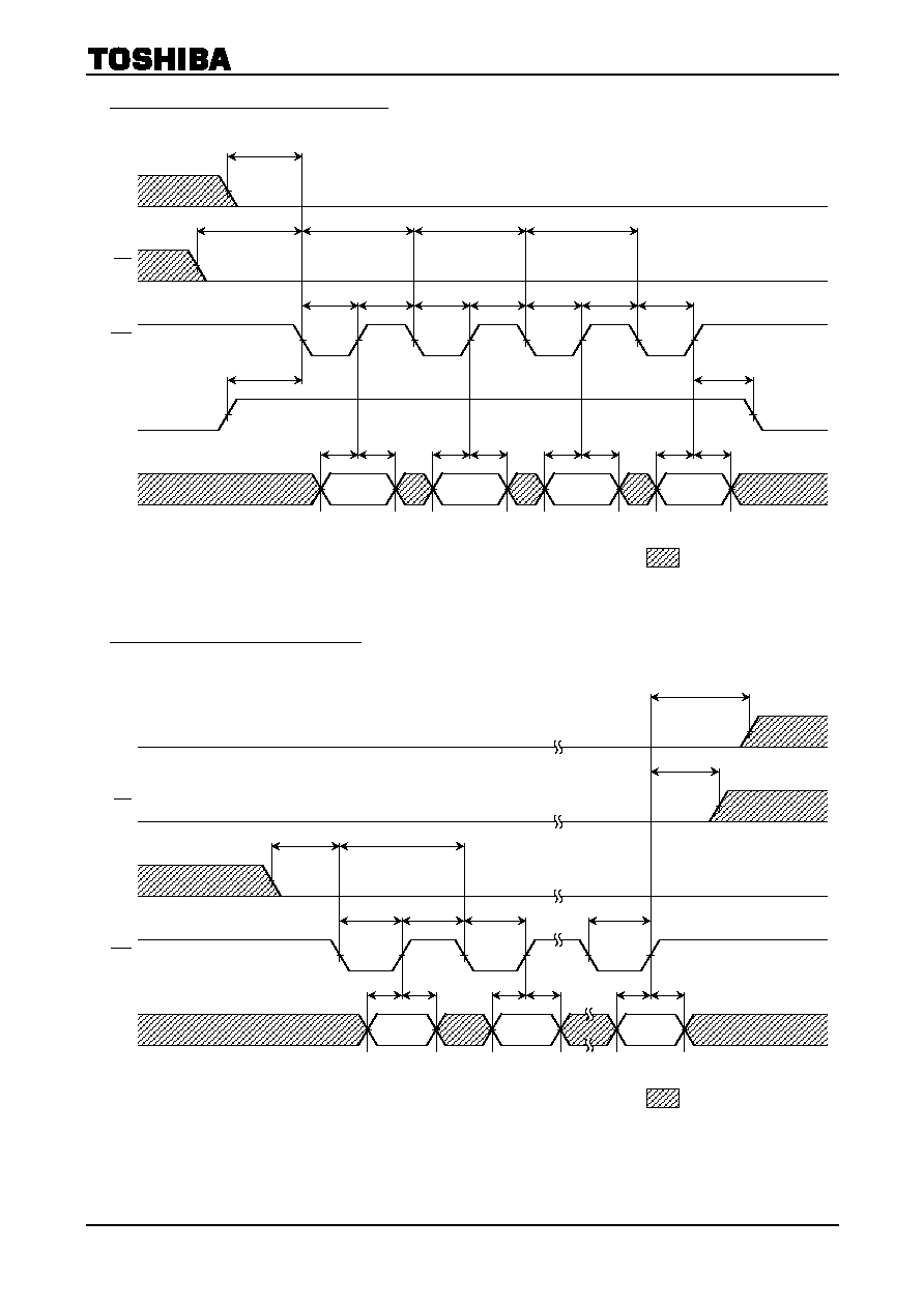
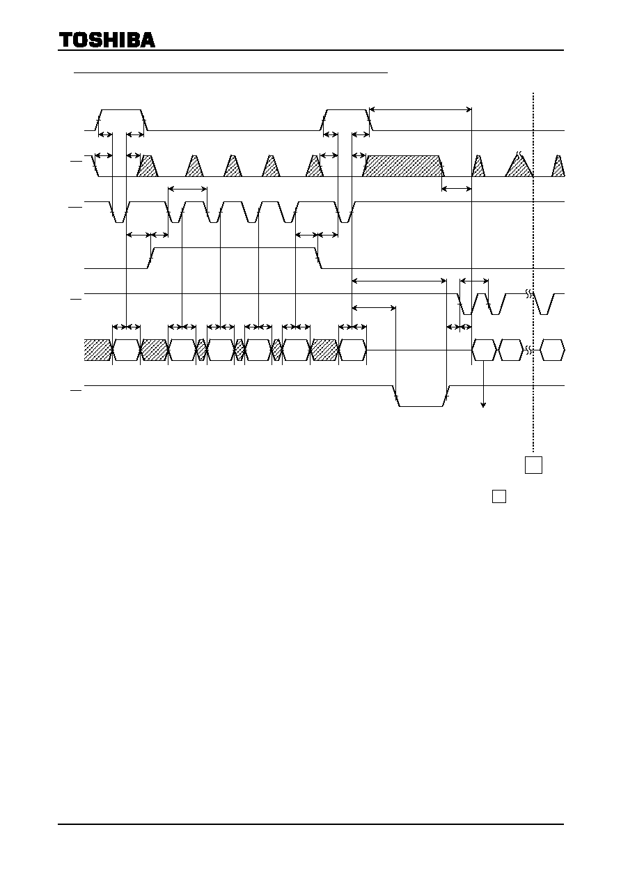
TIMING DIAGRAMS
Latch Timing Diagram for Command/Address/Data
Command Input Cycle Timing Diagram
CLE
ALE
CE
RE
WE
Hold Time
t
DH
Setup Time
t
DS
I/O1
to I/O8
: V
IH
or V
IL
t
CS
t
DH
t
DS
t
ALS
t
ALH
t
WP
t
CLS
t
CH
t
CLH
: V
IH
or V
IL
CE
CLE
WE
ALE
I/O1
to I/O8
TC58NVG0S3AFT05
2003-08-20A 7/33
Address Input Cycle Timing Diagram
Data Input Cycle Timing Diagram
PA0 to 7
CA8 to 11
: V
IH
or V
IL
t
DH
t
DS
t
CLS
CLE
t
ALS
t
WP
t
ALH
t
WH
t
WP
t
WH
t
WP
CA0 to 7
t
CS
t
WC
t
WC
CE
WE
ALE
I/O1
to I/O8
t
WP
t
WH
t
WC
t
DH
t
DS
t
DH
t
DS
PA8 to 15
t
DH
t
DS
: V
IH
or V
IL
WE
t
WP
t
WP
t
WH
t
WP
t
ALS
t
WC
t
DH
t
DS
D
IN
0
D
IN
1
t
CLH
t
CH
ALE
CLE
CE
I/O1
to I/O8
D
IN
2111
t
DH
t
DS
t
DH
t
DS

TC58NVG0S3AFT05
2003-08-20A 8/33
Serial Read Cycle Timing Diagram
Status Read Cycle Timing Diagram
t
REH
t
CHZ
CE
t
RHZ
t
REA
t
RC
t
RR
t
RHZ
t
REA
t
RHZ
t
REA
RE
BY
/
RY
I/O1
to I/O8
t
OH
t
OH
t
OH
t
RP
t
RP
t
RP
t
CEA
: V
IH
or V
IL
*
70h represents the hexadecimal number
t
WHR
WE
t
DH
t
DS
t
CLS
t
CLSTO
t
CS
t
CLH
t
CH
t
WP
Status
output
70h
*
t
WHC
t
CSTO
t
IR
t
RSTO
t
RHZ
t
CHZ
CE
CLE
RE
BY
/
RY
I/O1
to I/O8
t
OH

TC58NVG0S3AFT05
2003-08-20A 9/33
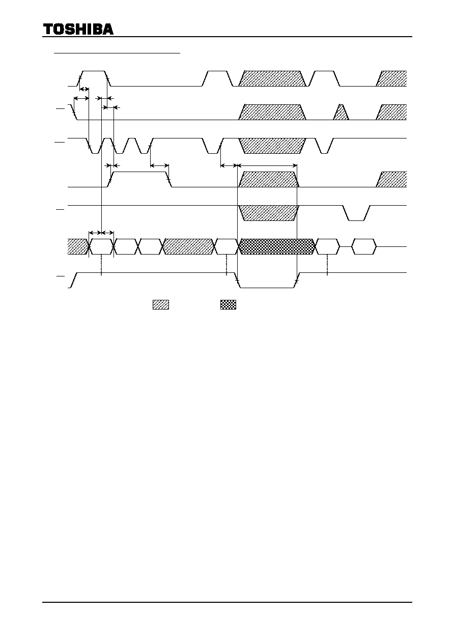
Read Cycle Timing Diagram
Read Cycle Timing Diagram: When Interrupted by
CE
t
CLEA
I/O1
to I/O8
t
CS
t
CLS
t
CLH
t
CH
00h
CA0 to 7
CA8 to 11
PA8 to 15
t
DH
t
DS
t
WC
t
ALS
t
ALH
t
R
WE
CLE
CE
ALE
RE
t
DH
t
DS
t
DH
t
DS
t
DH
t
DS
PA0 to 7
t
DH
t
DS
30h
t
DH
t
DS
t
ALH
t
WB
t
CS
t
CLS
t
CLH
t
CH
t
ALS
t
RC
D
OUT
N
D
OUT
N
+
1
t
RR
t
REA
t
CEA
Col. Add. N
Data out from
Col. Add. N
BY
/
RY
t
CLEA
I/O1
to I/O8
t
CS
t
CLS
t
CLH
t
CH
00h
CA0 to 7
CA8 to 11
PA8 to 15
t
DH
t
DS
t
WC
t
ALS
t
ALH
t
R
WE
CLE
CE
ALE
RE
t
DH
t
DS
t
DH
t
DS
t
DH
t
DS
PA0 to 7
t
DH
t
DS
30h
t
DH
t
DS
t
ALH
t
WB
t
CS
t
CLS
t
CLH
t
CH
t
ALS
t
RC
D
OUT
N
D
OUT
N
+
1
t
RR
t
REA
t
CEA
Col. Add. N
Col. Add. N
BY
/
RY
t
OH
t
RHZ
t
CHZ
TC58NVG0S3AFT05
2003-08-20A 10/33
Column Address Change in Read Cycle Timing Diagram (1/2)
t
CLEA
I/O1
to I/O8
t
CS
t
CLS
t
CLH
t
CH
00h
CA0 to 7
CA8 to 11
PA8 to 15
t
DH
t
DS
t
WC
t
ALS
t
ALH
t
R
CLE
CE
ALE
RE
t
DH
t
DS
t
DH
t
DS
t
DH
t
DS
Column address
A
PA0 to 7
t
DH
t
DS
30h
t
DH
t
DS
t
ALH
t
WB
t
CS
t
CLS
t
CLH
t
CH
t
ALS
t
RC
D
OUT
A
D
OUT
A
+
1
t
REA
D
OUT
A
+
N
1
t
CEA
t
RR
Continues to 1 of next page
Page address
P
Page address
P
Column address
A
WE
BY
/
RY

TC58NVG0S3AFT05
2003-08-20A 11/33
Column Address Change in Read Cycle Timing Diagram (2/2)
I/O1
to I/O8
t
CS
t
CLS
t
CLH
t
CH
05h
CA0 to 7
CA8 to 11
t
WC
t
ALS
t
ALH
CLE
CE
ALE
RE
t
DH
t
DS
t
DH
t
DS
t
DH
t
DS
Column address
B
E0h
t
DH
t
DS
t
ALH
t
CS
t
CLS
t
CLH
t
CH
t
ALS
D
OUT
B
D
OUT
B
+
1
t
REA
D
OUT
B
+
N'
1
D
OUT
A
+
N
t
RHW
Continued from 1 of last page
Page address
P
Column address
B
t
RC
t
CLEA
t
CEA
t
IR
WE
BY
/
RY

TC58NVG0S3AFT05
2003-08-20A 12/33
Auto-Program Operation Timing Diagram
t
DH
t
CLS
t
ALS
t
DS
t
DH
t
DS
t
DH
CA0 to 7
80h
WE
CLE
CE
ALE
RE
BY
/
RY
t
Prog
: V
IH
or V
IL
t
CLH
t
CH
t
CS
t
WB
t
DS
t
DS
t
DH
t
ALH
I/O1
to I/O8
t
ALH
t
ALS
D
IN
2111
Status
output
: Do not input data while data is being output.
CA8 to 11
t
CS
PA0 to 7 PA8 to 15
D
IN
0
D
IN
1
10h
70h
t
CLS
TC58NVG0S3AFT05
2003-08-20A 13/33
Auto Block Erase Timing Diagram
t
CS
60h
PA8 to 15
WE
CLE
CE
ALE
RE
BY
/
RY
: V
IH
or V
IL
t
CLS
t
CLH
t
CLS
PA0 to 7
t
DS
t
DH
t
ALS
: Do not input data while data is being output.
D0h
70h
t
WB
t
BERASE
Busy
Status Read
command
Erase Start
command
Auto Block
Erase Setup
command
I/O1
to I/O8
Status
output
t
ALH

TC58NVG0S3AFT05
2003-08-20A 14/33
ID Read Operation Timing Diagram
: V
IH
or V
IL
WE
CLE
RE
t
CEA
CE
ALE
I/O
t
ALEA
ID Read
command
Address
00
Maker code
Device code
t
REAID
t
CLS
t
CS
t
DH
t
CH
t
ALH
t
ALS
t
CLS
t
CS
t
CH
t
ALH
Note 1: 80h or 00h
Note 2: 95h or 15h
Note 3: 40h or C0h
t
DH
90h 00h
98h
t
REAID
F1h
t
REAID
t
REAID
t
REAID
Note 1
Note 2
Note 3
TC58NVG0S3AFT05
2003-08-20A 15/33
PIN FUNCTIONS
The device is a serial access memory which utilizes time-sharing input of address information. The device
pin-outs are configured as shown in Figure 1.
Command Latch Enable: CLE
The CLE input signal is used to control loading of the
operation mode command into the internal command register.
The command is latched into the command register from the
I/O port on the rising edge of the WE signal while CLE is
High.
Address Latch Enable: ALE
The ALE signal is used to control loading of either address
information or input data into the internal address/data
register.
Address information is latched on the rising edge of WE if
ALE is High.
Input data is latched if ALE is Low.
Chip Enable:
The device goes into a low-power Standby mode when CE goes High during the device is in Ready state.
The CE signal is ignored when device is in Busy state (
BY
/
RY
= L), such as during a Program or Erase or
Read operation, and will not enter Standby mode even if the CE input goes High.
Write Enable:
The WE signal is used to control the acquisition of data from the I/O port.
Read Enable:
The RE signal controls serial data output. Data is available t
REA
after the falling edge of RE .
The internal column address counter is also incremented (Address
= Address + 1) on this falling edge.
I/O Port: I/O1 to 8
The I/O1 to 8 pins are used as a port for transferring address, command and input/output data to and from
the device.
Write Protect:
The WP signal is used to protect the device from accidental programming or erasing. The internal voltage
regulator is reset when WP is Low. This signal is usually used for protecting the data during the power-on/off
sequence when input signals are invalid.
Ready/Busy:
The
BY
/
RY
output signal is used to indicate the operating condition of the device. The
BY
/
RY
signal is
in Busy state (
BY
/
RY
= L) during the Program, Erase and Read operations and will return to Ready state
(
BY
/
RY
= H) after completion of the operation. The output buffer for this signal is an open drain and has to
be pulled-up to Vccq with appropriate resister.
CE
WE
RE
WP
BY
/
RY
1
2
3
4
5
6
7
8
9
10
11
12
13
14
15
16
17
18
19
20
21
22
23
24
NC
NC
NC
NC
I/O8
I/O7
I/O6
I/O5
NC
NC
NC
V
CC
V
SS
NC
NC
NC
I/O4
I/O3
I/O2
I/O1
NC
NC
NC
NC
NC
NC
NC
NC
NC
GND
NC
NC
V
CC
V
SS
NC
NC
CLE
ALE
NC
NC
NC
NC
NC
WE
BY
/
RY
48
47
46
45
44
43
42
41
40
39
38
37
36
35
34
33
32
31
30
29
28
27
26
25
WP
RE
CE
Figure 1. Pinout
TC58NVG0S3AFT05
2003-08-20A 16/33
Schematic Cell Layout and Address Assignment
The Program operation works on page units while the Erase operation works on block units.
A page consists of 2112 bytes in which 2048 bytes are used
for main memory storage and 64 bytes are for redundancy
or for other uses.
1 page
= 2112 bytes
1 block
= 2112 bytes ◊ 64 pages = (128K + 4K) bytes
Capacity
= 2112 bytes ◊ 64 pages ◊ 1024 blocks
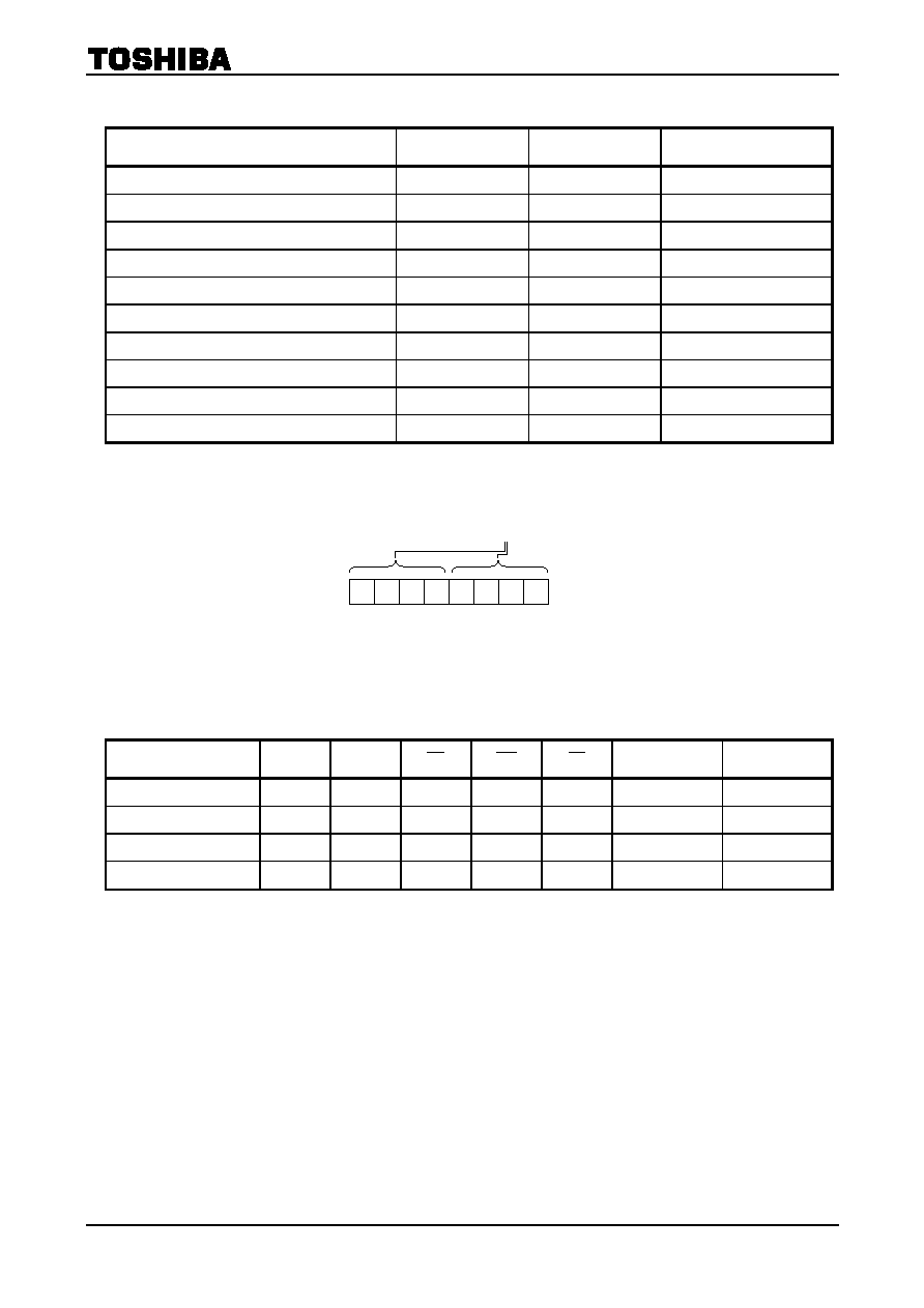
An address is read in via the I/O port over four consecutive
clock cycles, as shown in Table 1.
Table 1. Addressing
I/O8 I/O7 I/O6 I/O5 I/O4 I/O3 I/O2 I/O1
First
cycle
CA7 CA6 CA5 CA4 CA3 CA2 CA1 CA0
Second
cycle
L L L L
CA11
CA10
CA9
CA8
Third
cycle
PA7 PA6 PA5 PA4 PA3 PA2 PA1 PA0
CA0 to CA11 : Column address
PA0 to PA15 : Page address
PA6 to PA15 : Block address
PA0 to PA5 : NAND address in block
Fourth
cycle
PA15 PA14 PA13 PA12 PA11 PA10 PA9 PA8
Operation Mode: Logic and Command Tables
The operation modes such as Program, Erase, Read and Reset are controlled by the eleven different
command operations shown in Table 3. Address input, command input and data input/output are controlled by
the CLE, ALE, CE , WE , RE and WP signals, as shown in Table 2.
Table 2. Logic Table
CLE
ALE
CE
WE
RE
WP
*
1
Command Input
H
L
L
H
*
Data
Input
L L L H H
Address input
L
H
L
H
*
Serial
Data
Output
L L L H
*
During Programming (Busy)
* * * * *
H
During Erasing (Busy)
* * * * *
H
During Reading (Busy)
* * * * * *
Program, Erase Inhibit
* * * * *
L
Standby
* *
H
* *
0 V/V
CC
H: V
IH
, L: V
IL
,
*
: V
IH
or V
IL
*
1: Refer to Application Note (10) toward the end of this document regarding the WP signal when Program or Erase Inhibit
64 Pages
=
1 block
8I/O
2112
65536
pages
1024 blocks
I/O1
I/O8
64
2048
Figure 2. Schematic Cell Layout
TC58NVG0S3AFT05
2003-08-20A 17/33
Table 3. Command table (HEX)
First Cycle
Second Cycle
Acceptable while Busy
Serial Data Input
80
Auto Program
10
Read Address Input
00
Column Address Change in Serial Data Output
05
Read Start
30
Read Column Change
E0
Auto Block Erase
60
D0
ID Read
90
Status Read
70
Reset FF
Table 4. shows the operation states for Read mode.
Table 4. Read mode operation states
CLE
ALE
CE
WE
RE
I/O1 to I/O8
Power
Output select
L
L
L
H
L
Data output
Active
Output Deselect
L
L
L
H
H
High impedance
Active
Standby L
L
H
H
*
High impedance
Standby
Read Busy
* * * * *
High Impedance
Active
H: V
IH
, L: V
IL
,
*
: V
IH
or V
IL
0
0
0
0
0
0
0
I/O8
7 6 5 4 3 2 I/O1
Serial Data Input: 80h
(Example)
HEX data bit assignment
1

TC58NVG0S3AFT05
2003-08-20A 18/33
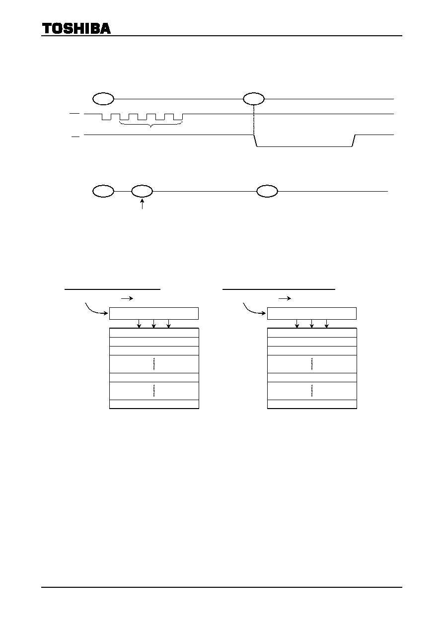
DEVICE OPERATION
Read Mode
Read mode is set when "00h" and "30h" commands are issued to the Command register. Between the
commands, start address for the Read mode need to be issued. Refer to Figure 3. below for sequence and the
block diagram (Refer to the detailed timing chart.).
Random Column Address Change in Read Cycle
A data transfer operation from the cell array to the register
starts on the rising edge of WE in the 30h command input
cycle (after the address information has been latched). The
device will be in Busy state during this transfer period.
After the transfer period the device returns to Ready state.
Serial data can be output synchronously with the RE clock
from the start address designated in the address input cycle.
Cell array
Select page
N
M
Figure 3. Read mode (1) operation
2111
BY
/
RY
WE
CLE
RE
00h
CE
ALE
I/O
Busy
30h
Page Address N
Column Address M
M M
+
1
M
+
2
Page Address N
Start-address input
In the serial data out from the register, the column address
can be changed by inputting the column address with 05h and
E0h commands.
The data are read out in serial from the column address
which is input to the device by 05h and E0h commands with
RE clock.
Cell array
Select page
N
M
Figure 4. Random Column Address Change in Serial Read
M'
Start-address input
BY
/
RY
WE
CLE
00h
CE
ALE
I/O
Busy
Page N
30h
05h E0h
Col. M
Page N
Col. M'
M M
+
1 M
+
2 M
+
3
M' M'
+
1 M'
+
2 M'
+
3 M'
+
4
Page N
Col. M
Start from Col. M
Start from Col. M'
RE

TC58NVG0S3AFT05
2003-08-20A 19/33
Auto Page Program Operation
The device carries out an Automatic Page Program operation when it receives a "10h" Program command
after the address and data have been input. The sequence of command, address and data input is shown below.
(Refer to the detailed timing chart.)
Auto Block Erase
The Auto Block Erase operation starts on the rising edge of WE after the Erase Start command "D0h"
which follows the Erase Setup command "60h". This two-cycle process for Erase operations acts as an extra
layer of protection from accidental erasure of data due to external noise. The device automatically executes the
Erase and Verify operations.
The data is transferred (programmed) from the register to the
selected page on the rising edge of WE following input of the "10h"
command. After programming, the programmed data is transferred
back to the register to be automatically verified by the device. If the
programming does not succeed, the Program/Verify operation is
repeated by the device until success is achieved or until the
maximum loop number set in the device is reached.
Figure 7. Auto Page Program operation
Data input
Selected
page
Reading & verification
Program
CLE
80h
ALE
I/O
Din
Page P
10h
CE
WE
Din
Col. M
Data
Status Out
RE
BY
/
RY
Din
Din
70h
Pass
I/O
Fail
BY
/
RY
60
D0
70
Block Address
input: 2 cycles
Status Read
command
Busy
Erase Start
command

TC58NVG0S3AFT05
2003-08-20A 20/33
ID Read
The device contains ID code which identify the device type, the manufacturer, and some features of the
device. The ID codes can be read out under the following timing conditions:
Table 6. Code table
Descripton
I/O8 I/O7 I/O6 I/O5 I/O4 I/O3 I/O2 I/O1
Hex
Data
1st
Data
Maker
Code
1 0 0 1 1 0 0 0
98h
2nd
Data
Device
Code
1 1 1 1 0 0 0 1
F1h
3rd Data
Chip Number, Cell Type,
PGM Page
0
or
1
0 0 0 0 0 0 0 80h
or
00h
4th Data
Page Size, Block Size,
Redundant Size, Organization
0
or
1
0 0 1 0 1 0 1 95h
or
15h
5th Data
Plane Number, Plane Size
0 or 1
1
0
0
0
0
0
0
40h or C0h
3rd Data
Descripton
I/O8 I/O7 I/O6 I/O5 I/O4 I/O3 I/O2 I/O1
1
0 0
2
0 1
4
1 0
Internal Chip Number
8
1 1
2 level cell
0
0
4 level cell
0
1
8 level cell
1
0
Cell Type
16
level
cell
1 1
1
0 0
2
0 1
4
1 0
Number of simultaneously
programmed pages
8
1 1
Reserved
1
0
Reserved 2
0 or 1
For the specifications of the access times t
REAID
, t
CR
and t
ALEA
refer to the AC Characteristics.
Figure 13. ID Read Timing
WE
CLE
RE
t
CEA
CE
ALE
I/O
t
ALEA
t
REAID
ID Read
command
Address
00
Maker code
Device code
90h
00h
98h
F1h Note
1 Note
2 Note
3
Note 1: 80h or 00h
Note 2: 95h or 15h
Note 3: 40h or C0h
TC58NVG0S3AFT05
2003-08-20A 21/33
4th Data
Descripton
I/O8 I/O7 I/O6 I/O5 I/O4 I/O3 I/O2 I/O1
1
KB
0 0
2
KB
0 1
4
KB
1 0
Page Size
(without redundant area)
8
KB
1 1
64
KB
0 0
128
KB
0 1
256
KB
1 0
Block Size
(without redundant area)
512
KB
1 1
8
0 0
16
0 1
Reserved
1 0
Redundant area size
(byte/512 byte)
Reserved
1 1
◊
8
0
Organization
◊
16
1
Reserved
0
or
1
5th Data
Descripton
I/O8 I/O7 I/O6 I/O5 I/O4 I/O3 I/O2 I/O1
1
0 0
2
0 1
4
1 0
Plane Number
8
1 1
64
Mbit
0
0 0
128
Mbit
0
0 1
256
Mbit
0
1 0
512
Mbit
0
1 1
1
Gbit
1
0 0
2
Gbit
1
0 1
4
Gbit
1
1 0
Plane Size
8
Gbit
1
1 1
Reserved
0 or 1
0
0

TC58NVG0S3AFT05
2003-08-20A 22/33
Status Read
The device automatically implements the execution and verification of the Program and Erase operations.
The Status Read function is used to monitor the Ready/Busy status of the device, determine the result (pass
/fail) of a Program or Erase operation, and determine whether the device is in Protect mode. The device status
is output via the I/O port on the RE clock after a "70h" command input.
The resulting information is outlined in Table 5.
Table 5. Status output table
STATUS
OUTPUT
I/O1
Chip Status 1
Pass: 0
Fail: 1
I/O2
Not Used
0 or 1
I/O3 Not
Used
0
I/O4 Not
Used
0
I/O5 Not
Used
0
I/O6 Ready/Busy
Ready:
1
Busy:
0
I/O7
Not Used
0 or 1
I/O8
Write Protect
Protect: 0
Not Protected: 1
The Pass/Fail status on I/O1 is only
valid when the device is in the Ready
state.
An application example with multiple devices is shown in Figure 6.
System Design Note: If the
BY
/
RY
pin signals from multiple devices are wired together as shown in the
diagram, the Status Read function can be used to determine the status of each individual device.
WE
RE
Status on Device 1
70h
1
CE
ALE
I/O
70h
Status on Device N
BY
/
RY
CLE
N
CE
Figure 6. Status Read timing application example
Busy
Device
1
CLE
1
CE
Device
2
2
CE
3
CE
Device
N
N
CE
Device
N
+
1
1
N
CE
+
ALE
WE
RE
I/O1
to I/O8
BY
/
RY
Device
3

TC58NVG0S3AFT05
2003-08-20A 23/33
Reset
The Reset mode stops all operations. For example, in the case of a Program or Erase operation the internally
generated voltage is discharged to 0 volts and the device enters Wait state.
The response to an "FFh" Reset command input during the various device operations is as follows:
When a Reset (FFh) command is input during programming
When a Reset (FFh) command is input during erasing
When a Reset (FFh) command is input during Read operation
When a Status Read command (70h) is input after a Reset
When two or more Reset commands are input in succession
Internal V
PP
80
10
FF
00
BY
/
RY
t
RST
(max 10
µ
s)
Figure 8.
Internal erase
voltage
D0
FF
00
BY
/
RY
t
RST
(max 500
µ
s)
Figure 9.
00
FF
00
BY
/
RY
t
RST
(max 6
µ
s)
Figure 10.
Figure 11.
FF
70
BY
/
RY
I/O status : Pass/Fail
Pass
: Ready/Busy
Ready
FF
70
BY
/
RY
I/O status : Ready/Busy
Busy
Figure 12.
BY
/
RY
FF
FF
(3)
(2)
(1)
The second command is invalid, but the third command is valid.
FF
FF
FF

TC58NVG0S3AFT05
2003-08-20A 24/33
APPLICATION NOTES AND COMMENTS
(1) Power-on/off
sequence:
The timing sequence shown in Figure 15 is necessary for power-on/off sequence.
The device internal initialization start after the power supply reaches appropriate level in power on
sequence. During the initialization the device Ready/Busy signal outputs Busy state as shown in the Figure
15. In this time period, the acceptable commands are FFh or 70h.
The WP signal is useful for protecting against data corruption at power-on/off.
(2)
Status after power-on
The following sequence is necessary because some input signals may not be stable at power-on.
(3)
Prohibition of unspecified commands
The operation commands are listed in Table 3. Input of a command other than those specified in Table 3.
is prohibited. Stored data may be corrupted if an unknown command is entered during the command cycle.
(4)
Restriction of command while Busy state
During Busy state, do not input any command except 70h, and FFh.
V
IL
Operation
0 V
V
CC
2.7 V
2.5 V
V
IL
Don't
care
Don't
care
Figure 15. Power-on/off Sequence
V
IH
CE
, WE , RE
WP
CLE, ALE
Invalid
Don't
care
Ready/Busy
1 ms max
100
µ
s max
FF
Reset
Power on
Figure 16.
TC58NVG0S3AFT05
2003-08-20A 25/33
(5)
Acceptable commands after Serial Input command "80h"
Once the Serial Input command "80h" has been input, do not input any command other than the Column
Address Change in Auto Program command "10h" or the Reset command "FFh".
If a command other than "10h" or "FFh" is input, the Program operation is not performed and the device
operation is set to the mode which the input command specifies.
(6)
Addressing for program operation
Within a block, the pages must be programmed consecutively from the LSB (least significant bit) page of
the block to MSB (most significant bit) page of the block. Random page address programming is prohibited.
WE
BY
/
RY
80
FF
Address input
Command other than
"10h" or "FFh"
80
Programming cannot be executed.
10
XX
Mode specified by the command.
DATA IN: Data (1)
Page 0
Data register
Page 2
Page 1
Page 31
Page 63
(1)
(2)
(3)
(32)
(64)
Data (64)
From the LSB page to MSB page
DATA IN: Data (1)
Page 0
Data register
Page 2
Page 1
Page 31
Page 63
(2)
(32)
(3)
(1)
(64)
Data (64)
Ex.) Random page program (Prohibition)
Figure 17. page programming within a block
TC58NVG0S3AFT05
2003-08-20A 26/33
(7)
Status Read during a Read operation
The device status can be read out by inputting the Status Read command "70h" in Read mode.
Once the device has been set to Status Read mode by a "70h" command, the device will not return to
Read mode.
Therefore, a Status Read during a Read operation is prohibited.
However, when the Read command "00h" is input during [A], Status mode is reset and the device returns
to Read mode. In this case, data output starts automatically from address N and address input is
unnecessary
(8)
Auto programming failure
(9)
BY
/
RY
: termination for the Ready/Busy pin (
BY
/
RY
)
A pull-up resistor needs to be used for termination because the
BY
/
RY
buffer consists of an open drain
circuit.
00
Address N
command
CE
WE
BY
/
RY
RE
[A]
Status Read
command input
Status Read
Status output
Figure 18.
70
00
30
Fail
80
10
80
10
Address
M
Data
input
70
I/O
Address
N
Data
input
If the programming result for page address M is Fail, do not try to program the
page to address N in another block without the data input sequence.
Because the previous input data has been lost, the same input sequence of 80h
command, address and data is necessary.
10
80
Figure 19.
M
N
Figure 19.
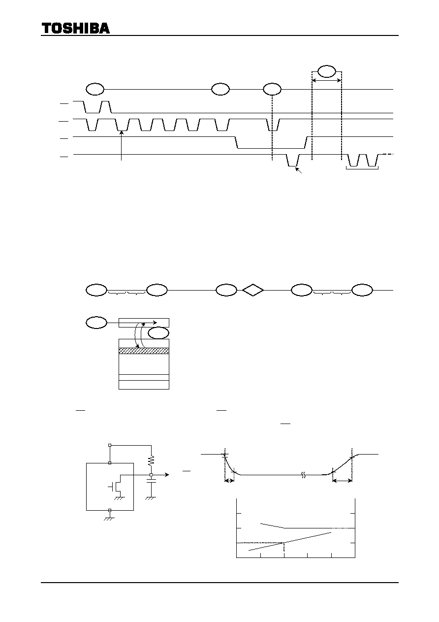
This data may vary from device to device.
We recommend that you use this data as a
reference when selecting a resistor value.
V
CC
V
CC
Device
V
SS
R
BY
/
RY
C
L
1.5
µ
s
1.0
µ
s
0.5
µ
s
0
1 K
4
K
3 K
2 K
15 ns
10 ns
5 ns
t
f
t
r
R
t
r
t
f
V
CC
=
3.3 V
Ta
=
25∞C
C
L
=
100 pF
t
f
Ready
3.0 V
V
CC
1.0 V
t
r
3.0 V
1.0 V
Busy

TC58NVG0S3AFT05
2003-08-20A 27/33
(10)
Note regarding the WP signal
The Erase and Program operations are automatically reset when WP goes Low. The operations are
enabled and disabled as follows:
Enable Programming
Disable Programming
Enable Erasing
Disable Erasing
WP
t
WW
(100 ns min)
80
10
WE
BY
/
RY
DIN
WP
t
WW
(100 ns min)
80
10
WE
BY
/
RY
DIN
WP
t
WW
(100 ns min)
60
D0
WE
BY
/
RY
DIN
WP
t
WW
(100 ns min)
60
D0
WE
BY
/
RY
DIN

TC58NVG0S3AFT05
2003-08-20A 28/33
(11)
When five address cycles are input
Although the device may read in a fifth address, it is ignored inside the chip.
Read operation
Program operation
Figure 22.
CLE
Address input
00h
CE
WE
ALE
I/O
BY
/
RY
Ignored
30h
CLE
CE
WE
ALE
I/O
Figure 23.
Data input
80h
Ignored
Address input
TC58NVG0S3AFT05
2003-08-20A 29/33
(12)
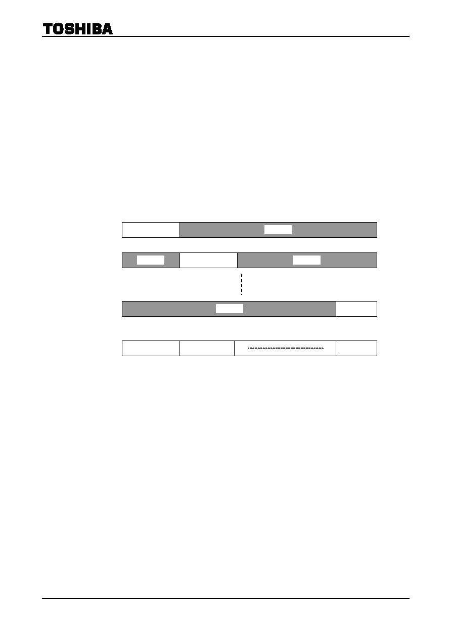
Several programming cycles on the same page (Partial Page Program)
A page can be divided into up to 8 segments as follows:-
Data area (column address 0 to 2047): 512 bytes
◊ 4 segments
1st
segment: column address 0 to 511
2nd segment: column address 512 to 1023
3rd segment: column address 1024 to 1535
4th segment: column address 1536 to 2047
Redundant area (column address 2048 to 2111): 16 bytes
◊ 4 segments
1st segment: column address 2048 to 2063
2nd segment: column address 2064 to 2079
3rd segment: column address 2080 to 2095
4th segment: column address 2096 to 2111
Each segment can be programmed individually as follows:
Note: The input data for unprogrammed or previously programmed page segments must be "1"
(i.e. the inputs for all page bytes outside the segment which is to be programmed should be set to all "1").
Data Pattern 8
Data Pattern 1
All 1 s
All 1 s
All 1 s
All 1 s
Figure 24.
1st programming
Result
Data Pattern 1
Data Pattern 2
Data Pattern 8
Data Pattern 2
2nd programming
8th programming
TC58NVG0S3AFT05
2003-08-20A 30/33
(13)
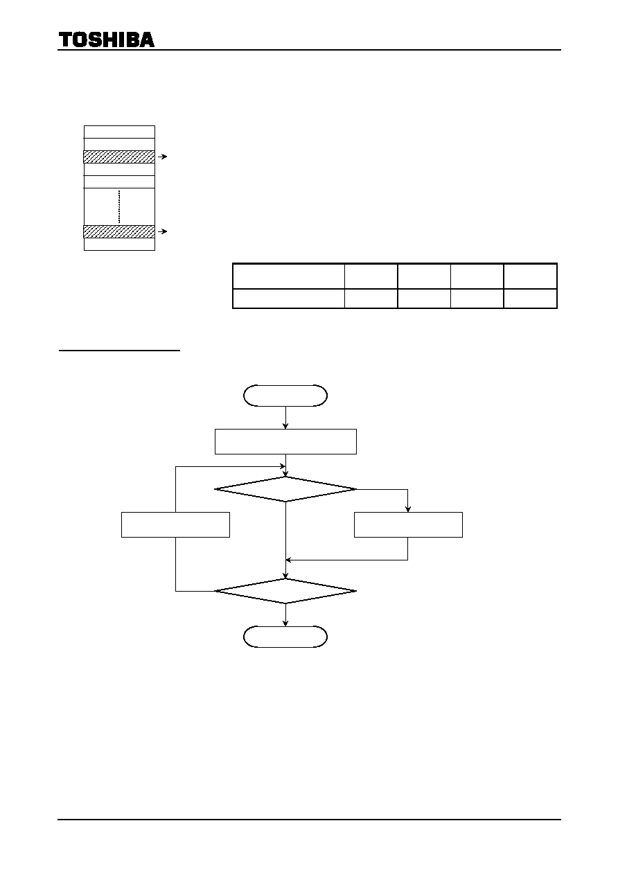
Invalid blocks (bad blocks)
The device occasionally contains unusable blocks. Therefore, the following issues must be recognized:
At the time of shipment, all data bytes in a valid block are FFh. For
bad blocks, all bytes are not in the FFh state. Please don't perform erase
operation to bad blocks.
Check if the device has any bad blocks after installation into the
system. Figure 27. shows the test flow for bad block detection. Bad blocks
which are detected by the test flow must be managed as unusable blocks
by the system.
A bad block does not affect the performance of good blocks because it is
isolated from the bit line by the select gate
The number of valid blocks at the time of shipment is as follows:
MIN
TYP.
MAX
UNIT
Valid (Good) Block Number
1004
1024
Block
Bad Block Test Flow
Bad Block
Bad Block
Figure 26.
Read Check: Read the 1st page or the 2nd
page of each block. If the column
address 0 or 2048 of the 1st
page or the 2nd page is not FF
(Hex), define the block as a bad
block.
Figure 27.
*
1: No erase operation is allowed to detected bad blocks
Pass
Read Check
Start
Bad Block
*
1
Block No.
=
1024
End
Yes
Fail
Block No
=
1
No
Block No.
=
Block No.
+
1

TC58NVG0S3AFT05
2003-08-20A 31/33
(14)
Failure phenomena for Program and Erase operations
The device may fail during a Program or Erase operation.
The following possible failure modes should be considered when implementing a highly reliable system.
FAILURE MODE
DETECTION AND COUNTERMEASURE SEQUENIE
Block
Erase Failure
Status Read after Erase
Block Replacement
Page
Programming Failure
Status Read after Program
Block Replacement
(1) Block Verify after Program
Retry
Single Bit
Programming Failure
"1 to 0"
(2) ECC
∑ ECC: Error Correction Code.
∑ Block Replacement
Program
Erase
When an error occurs in an Erase operation, prevent future accesses to this bad block
(again by creating a table within the system or by using another appropriate scheme).
(15)
Do not turn off the power before write/erase operation is complete. Avoid using the device when the battery
is low. Power shortage and/or power failure before write/erase operation is complete will cause loss of data
and/or damage to data.
When an error happens in Block A, try to
reprogram the data into another Block (Block
B) by loading from an external buffer. Then,
prevent further system accesses to Block A (by
creating a bad block table or by using another
appropriate scheme).
Block A
Block B
Error occurs
Buffer
memory
Figure 28.

TC58NVG0S3AFT05
2003-08-20A 32/33
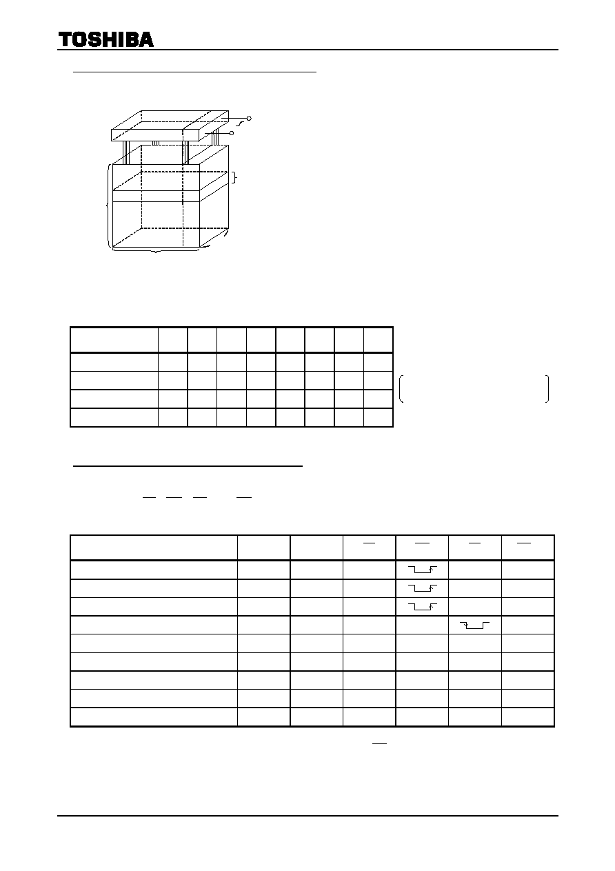
Package Dimensions
Weight: 0.53 g (typ.)

TC58NVG0S3AFT05
2003-08-20A 33/33
∑
The information contained herein is subject to change without notice.
∑
The information contained herein is presented only as a guide for the applications of our products. No
responsibility is assumed by TOSHIBA for any infringements of patents or other rights of the third parties which
may result from its use. No license is granted by implication or otherwise under any patent or patent rights of
TOSHIBA or others.
∑
TOSHIBA is continually working to improve the quality and reliability of its products. Nevertheless, semiconductor
devices in general can malfunction or fail due to their inherent electrical sensitivity and vulnerability to physical
stress. It is the responsibility of the buyer, when utilizing TOSHIBA products, to comply with the standards of
safety in making a safe design for the entire system, and to avoid situations in which a malfunction or failure of
such TOSHIBA products could cause loss of human life, bodily injury or damage to property.
In developing your designs, please ensure that TOSHIBA products are used within specified operating ranges as
set forth in the most recent TOSHIBA products specifications. Also, please keep in mind the precautions and
conditions set forth in the "Handling Guide for Semiconductor Devices," or "TOSHIBA Semiconductor Reliability
Handbook" etc..
∑
The TOSHIBA products listed in this document are intended for usage in general electronics applications
(computer, personal equipment, office equipment, measuring equipment, industrial robotics, domestic appliances,
etc.). These TOSHIBA products are neither intended nor warranted for usage in equipment that requires
extraordinarily high quality and/or reliability or a malfunction or failure of which may cause loss of human life or
bodily injury ("Unintended Usage"). Unintended Usage include atomic energy control instruments, airplane or
spaceship instruments, transportation instruments, traffic signal instruments, combustion control instruments,
medical instruments, all types of safety devices, etc.. Unintended Usage of TOSHIBA products listed in this
document shall be made at the customer's own risk.
∑
The products described in this document are subject to the foreign exchange and foreign trade laws.
∑
TOSHIBA products should not be embedded to the downstream products which are prohibited to be produced
and sold, under any law and regulations.
030619EBA
RESTRICTIONS ON PRODUCT USE