TD62001~004APG/AFG
2002-12-11
1
TOSHIBA Bipolar Digital Integrated Circuit Silicon Monolithic
TD62001APG,TD62001AFG,TD62002APG,TD62002AFG,
TD62003APG,TD62003AFG,TD62004APG,TD62004AFG
7-channel Darlington Sink Driver
The TD62001APG/AFG Series are high-voltage, high-current
darlington drivers comprised of seven NPN darlington pairs.
All units feature integral clamp diodes for switching inductive
loads.
Applications include relay, hammer, lamp and display (LED)
drivers.
Features
l Output current (single output): 500 mA (max)
l High sustaining voltage output: 50 V (min)
l Output clamp diodes
l Inputs compatible with various types of logic
l Package type
APG: DIP-16 pin (Pb free package)
AFG: SOP-16 pin (Pb free package)
Type
Input base resistor
Designation
TD62001APG/AFG External
General
purpose
TD62002APG/AFG
10.5-k + 7-V
Zenner diode
14-V to 25-V PMOS
TD62003APG/AFG 2.7
k
TTL, 5-V CMOS
TD62004APG/AFG 10.5
k
6-V to 15-V PMOS,
CMOS
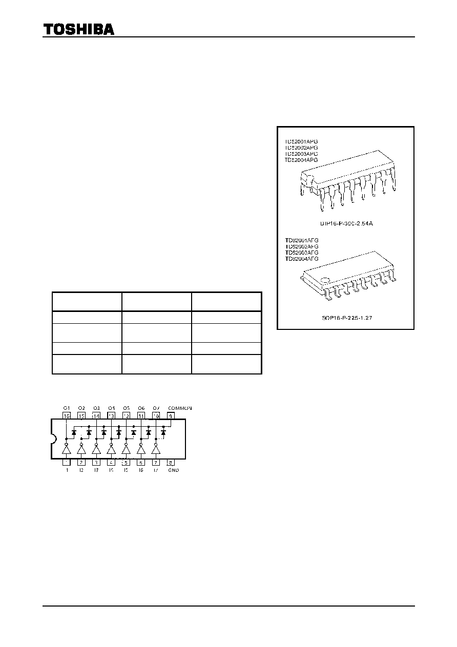
Pin Connection
(top view)
Weight
DIP16-P-300-2.54A : 1.11 g (Typ.)
SOP16-P-225-1.27 : 0.16 g (Typ.)

TD62001~004APG/AFG
2002-12-11
2
Schematics
(each driver)
TD62001APG/AFG TD62002APG/AFG
TD62003PAPG/AFG
TD62004APG/AFG
Note:
The input and output parasitic diodes cannot be used as clamp diodes.
Maximum Ratings
(Ta = 25�C)
Characteristics Symbol
Rating
Unit
Output sustaining voltage
V
CE (SUS)
-0.5 to 50
V
Output current
I
OUT
500 mA/ch
Input voltage
V
IN
(Note 1)
-0.5 to 30
V
Input current
I
IN
(Note 2)
25 mA
Clamp diode reverse voltage
V
R
50 V
Clamp diode forward current
I
F
500 mA
APG 1.47
Power dissipation
AFG
P
D
0.625
(Note
3)
W
Operating temperature
T
opr
-40 to 85
�C
Storage temperature
T
stg
-55 to 150
�C
Note 1: Except TD62001APG/AFG
Note 2: Only TD62001APG/AFG
Note 3: When mounted on a glass-epoxy PCB (30 mm
� 30 mm � 1.6 mm, Cu area: 50%)

TD62001~004APG/AFG
2002-12-11
3
Recommended Operating Conditions
(Ta = -40�C to 85�C)
Characteristics Symbol Condition
Min
Typ.
Max
Unit
Output sustaining voltage
V
CE (SUS)
0
50 V
Duty = 10%
0
370
APG
Duty = 50%
0
130
Duty = 10%
0
233
Output current
AFG
I
OUT
T
pw
= 25 ms
7 circuits
Ta = 85�C
T
j
= 120�C
Duty = 50%
0
70
mA/ch
Input voltage
Except
TD62001APG/
AFG
V
IN
0
24 V
TD62002 14.5
24
TD62003 2.8
24
Input voltage (output on)
TD62004
V
IN (ON)
I
OUT
= 400 mA
h
FE
= 800
6.2
24
V
TD62001
0
0.6
TD62002
0
7.4
TD62003
0
0.7
Input voltage (output off)
TD62004
V
IN (OFF)
0
1.0
V
Input current
Only TD62001
I
IN
0
10 mA
Clamp diode reverse voltage
V
R
50 V
Clamp diode forward current
I
F
350
mA
APG Ta
=
85�C
0.76
Power dissipation
AFG
P
D
Ta = 85�C
(Note)
0.325
W
Note: When mounted on a glass-epoxy PCB (30 mm
� 30 mm � 1.6 mm, Cu area: 50%)

TD62001~004APG/AFG
2002-12-11
4
Electrical Characteristics
(Ta = 25�C unless otherwise noted)
Characteristics Symbol
Test
Circuit
Test Condition
Min
Typ.
Max
Unit
V
CE
= 50 V, Ta = 25�C
50
Ooutput leakage current
I
CEX
1
V
CE
= 50 V, Ta = 85�C
100
mA
I
OUT
= 350 mA, I
IN
= 500
mA
1.3 1.6
I
OUT
= 200 mA, I
IN
= 350
mA
1.1 1.3
Collector-emitter saturation voltage
V
CE (sat)
2
I
OUT
= 100 mA, I
IN
= 250
mA
0.9 1.1
V
DC current transfer ratio
h
FE
2 V
CE
= 2 V, I
OUT
= 350 mA
1000
TD62002 V
IN
= 20 V, I
OUT
= 350 mA
1.1 1.7
TD62003 V
IN
= 2.4 V, I
OUT
= 350 mA
0.4 0.7
Input current (output on)
TD62004
I
IN (ON)
3
V
IN
= 9.5 V, I
OUT
= 350 mA
0.8 1.2
mA
Input current (output off)
I
IN (OFF)
4 I
OUT
= 500
mA, Ta = 85�C
50
65
mA
I
OUT
= 350 mA
13.7
TD62002
I
OUT
= 200 mA
11.4
I
OUT
= 350 mA
2.6
TD62003
I
OUT
= 200 mA
2.0
I
OUT
= 350 mA
4.7
Input voltage (output on)
TD62004
V
IN (ON)
5
V
CE
= 2 V
h
FE
= 800
I
OUT
= 200 mA
4.4
V
V
R
= 50 V, Ta = 25�C
50
Clamp diode reverse current
I
R
6
V
R
= 50 V, Ta = 85�C
100
mA
Clamp diode forward voltage
V
F
7 I
F
= 350 mA
2.0 V
Input capacitance
C
IN
15 pF
Turn-on delay
t
ON
8
V
OUT
= 50 V, R
L
= 125
W
C
L
= 15 pF
0.1
Turn-off delay
t
OFF
8
V
OUT
= 50 V, R
L
= 125
W
C
L
= 15 pF
0.2
ms

TD62001~004APG/AFG
2002-12-11
5
Test Circuit
1. I
CEX
2. V
CE
(sat)
, h
FE
3.
IIN (ON)
4. I
IN (OFF)
5. V
IN (ON)
6. I
R
7. V
F