TOSHIBA
TOSHIBA CORPORATION
MW50750196
1/5
MICROWAVE POWER GaAs FET
TIM5964-8SL
The information contained here is subject to change without notice.
The information contained herein is presented only as guide for the applications of our products. No responsibility is assumed by TOSHIBA for any infringements of patents or other rights of the third parties
which may result from its use. No license is granted by implication or otherwise under any patent or patent rights of TOSHIBA or others. These TOSHIBA products are intended for usage in general electronic
equipments (office equipment, communication equipment, measuring equipment, domestic electrification, etc.) Please make sure that you consult with us before you use these TOSHIBA products in equip-
ments which require high quality and/or reliability, and in equipments which could have major impact to the welfare of human life (atomic energy control, spaceship, traffic signal, combustion control, all types
of safety devices, etc.). TOSHIBA cannot accept liability to any damage which may occur in case these TOSHIBA products were used in the mentioned equipments without prior consultation with TOSHIBA.
High Efficiency and Low Distortion Internally Matched Power GaAs FETs (C-Band)
Features
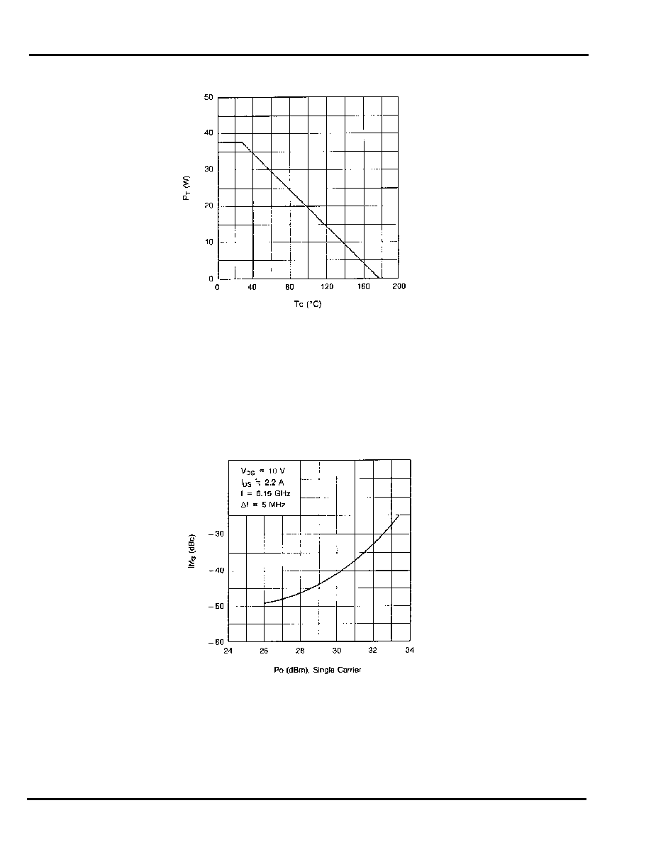
· Low intermodulation distortion
- IM
3
= -45 dBc at Po = 28.5 dBm, Single Carrier Level
· High power
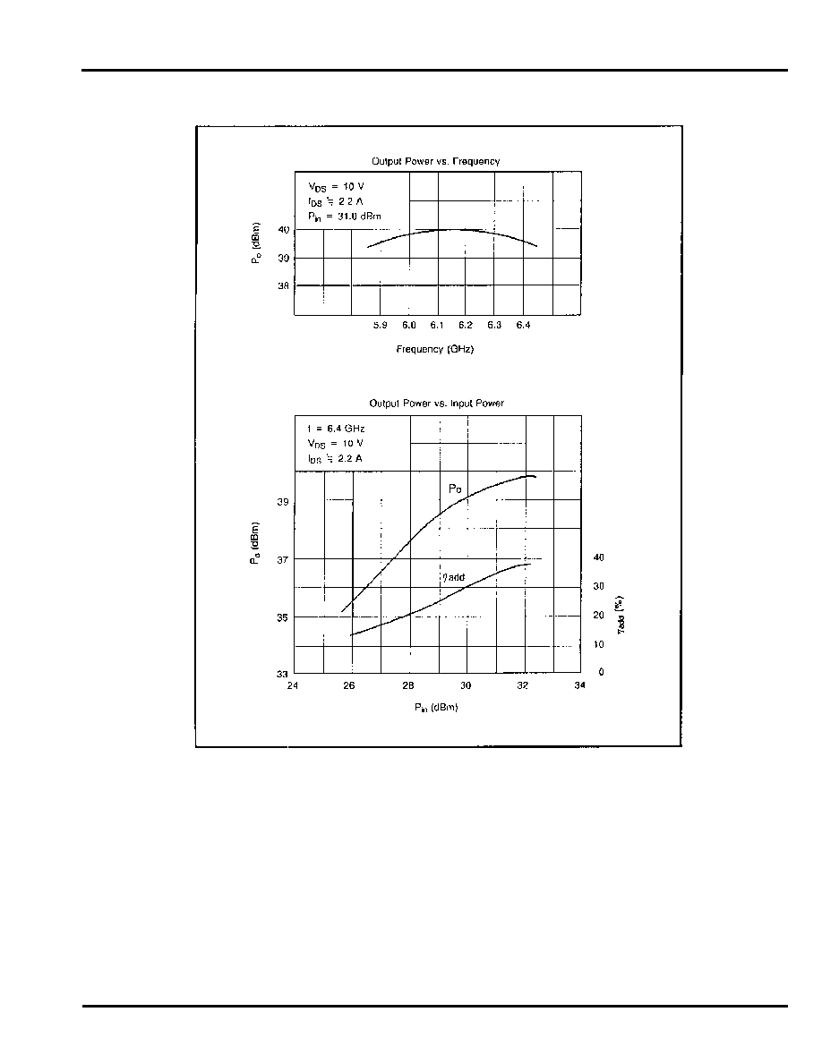
- P
1dB
= 39.5 dBm at 5.9 GHz to 6.4 GHz
· High gain
- G
1dB
= 8.5 dB at 5.9 GHz to 6.4 GHz
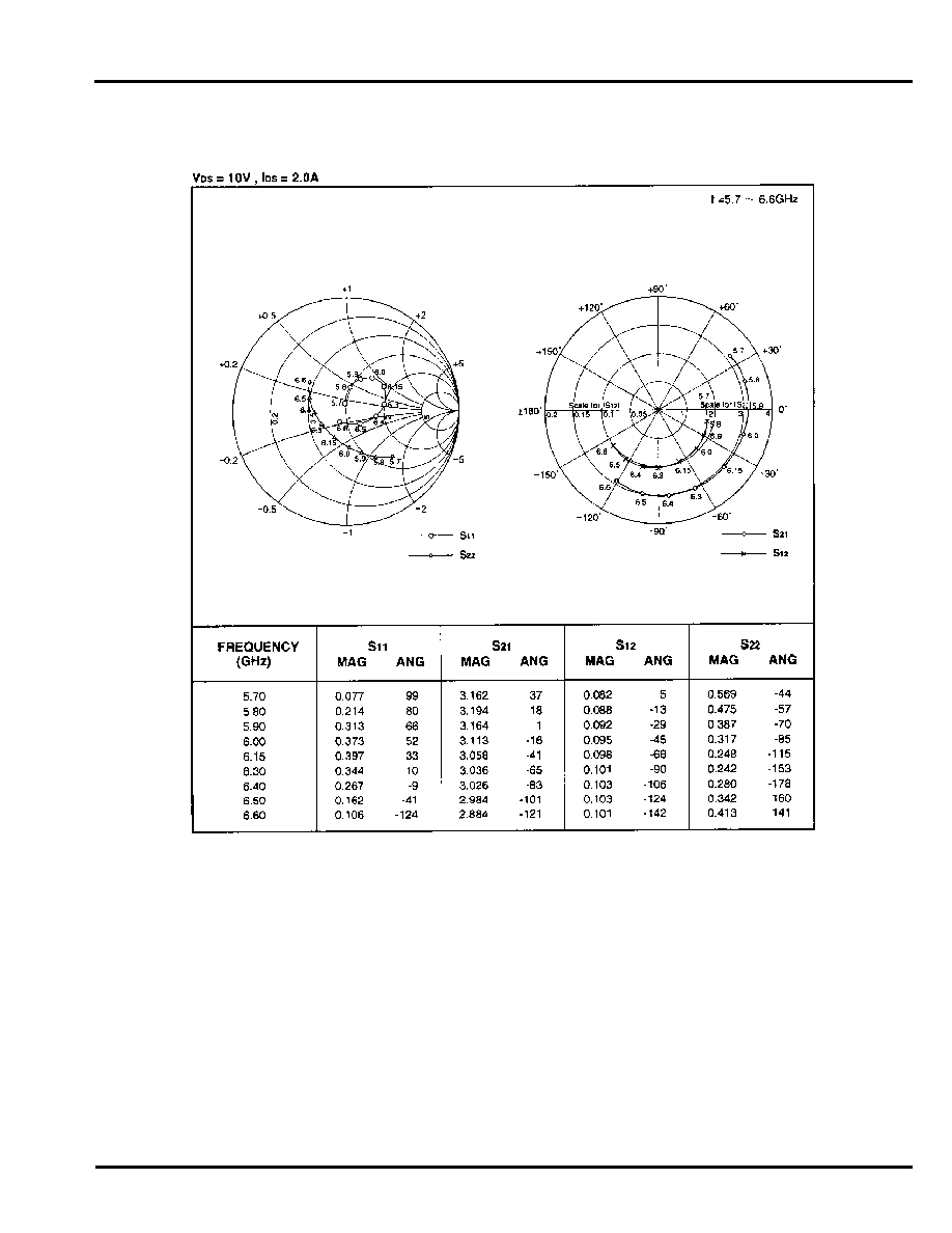
· Broadband internally matched
· Hermetically sealed package
RF Performance Specifications (T
a
= 25
°
C)
Electrical Characteristics (T
a
= 25
°
C)
Note 1: 2-tone Test Pout = 28.5 dBm Single Carrier Level.
Characteristic
Symbol
Condition
Unit
Min.
Typ.
Max.
Output Power at 1dB Compression
Point
P
1dB
V
DS
= 10V
f = 5.9 ~ 6.4 GHz
dBm
38.5
39.5
Power Gain at 1dB Compression
Point
G
1dB
dB
7.5
8.5
Drain Current
I
DS
A
2.2
2.6
Gain Flatness
G
dB
±
0.6
Power Added Efficiency
add
%
35
3rd Order Intermodulation Distortion
IM
3
Note 1
dBc
-42
-45
Channel-Temperature Rise
T
ch
V
DS
x I
DS
x R
th (c-c)
°
C
80
Characteristic
Symbol
Condition
Unit
Min.
Typ.
Max.
Transconductance
gm
V
DS
= 3V
I
DS
= 3.0A
mS
1800
Pinch-off Voltage
V
GSoff
V
DS
= 3V
I
DS
= 30 mA
V
-1
-2.5
-4.0
Saturated Drain Current
I
DSS
V
DS
= 3V
V
GS
= 0V
A
5.2
7.0
Gate-Source Breakdown Voltage
V
GSO
I
GS
= -100
µ
A
V
-5
Thermal Resistance
R
th (c-c)
Channel
to Case
°
C/W
2.5
3.8
2/5
MW50750196
TOSHIBA CORPORATION
TIM5964-8SL
Absolute Maximum Ratings (T
a
= 25
°
C)
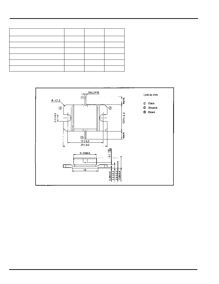
Package Outline (2-11D1B)
Handling Precautions for Packaged Type
Soldering iron should be grounded and the operating time should not exceed 10 seconds at 260
°
C
.
Characteristic
Symbol
Unit
Rating
Drain-Source Voltage
V
DS
V
15
Gate-Source Voltage
V
GS
V
-5
Drain Current
I
D
A
7.0
Total Power Dissipation (T
c
= 25
°
C)
P
T
W
37.5
Channel Temperature
T
ch
°C
175
Storage Temperature
T
stg
°C
-65 ~ 175