 | –≠–ª–µ–∫—Ç—Ä–æ–Ω–Ω—ã–π –∫–æ–º–ø–æ–Ω–µ–Ω—Ç: TK19H50C | –°–∫–∞—á–∞—Ç—å:  PDF PDF  ZIP ZIP |
TK19H50C
2005-08-23
1
TOSHIBA Field Effect Transistor Silicon N-Channel MOS Type (-MOS VI)
TK19H50C
Switching Regulator Applications
Low drain-source ON resistance
: R
DS
(ON)
= 0. 25
(typ.)
High forward transfer admittance
: |Y
fs
| = 14 S (typ.)
Low leakage current
: I
DSS
= 100
µA (max) (V
DS
= 500 V)
Enhancement mode
: V
th
= 2.0~4.0 V (V
DS
= 10 V, I
D
= 1 mA)
Maximum Ratings
(Ta = 25∞C)
Characteristic Symbol
Rating
Unit
Drain-source voltage
V
DSS
500 V
Drain-gate voltage (R
GS
= 20 k) V
DGR
500
V
Gate-source voltage
V
GSS
±30 V
DC (Note
1)
I
D
19
A
Drain current
Pulse (Note 1)
I
DP
76 A
Drain power dissipation (Tc = 25∞C)
P
D
150
W
Single-pulse avalanche energy
(Note
2)
E
AS
968
mJ
Avalanche current
I
AR
19 A
Repetitive avalanche energy (Note 3)
E
AR
15
mJ
Channel temperature
T
ch
150
∞C
Storage temperature range
T
stg
-55~150 ∞C
Thermal Characteristics
Characteristic Symbol
Max
Unit
Thermal resistance, channel to case
R
th (ch-c)
0.833 ∞C
/
W
Thermal resistance, channel to
ambient
R
th (ch-a)
50 ∞C
/
W
Note 1: Ensure that the channel temperature does not exceed 150∞C.
Note 2: V
DD
= 90 V, T
ch
= 25∞C (initial), L = 4.56 mH, R
G
= 25 , I
AR
= 19 A
Note 3: Repetitive rating: pulse width limited by maximum channel temperature
This transistor is an electrostatic-sensitive device. Handle with care.
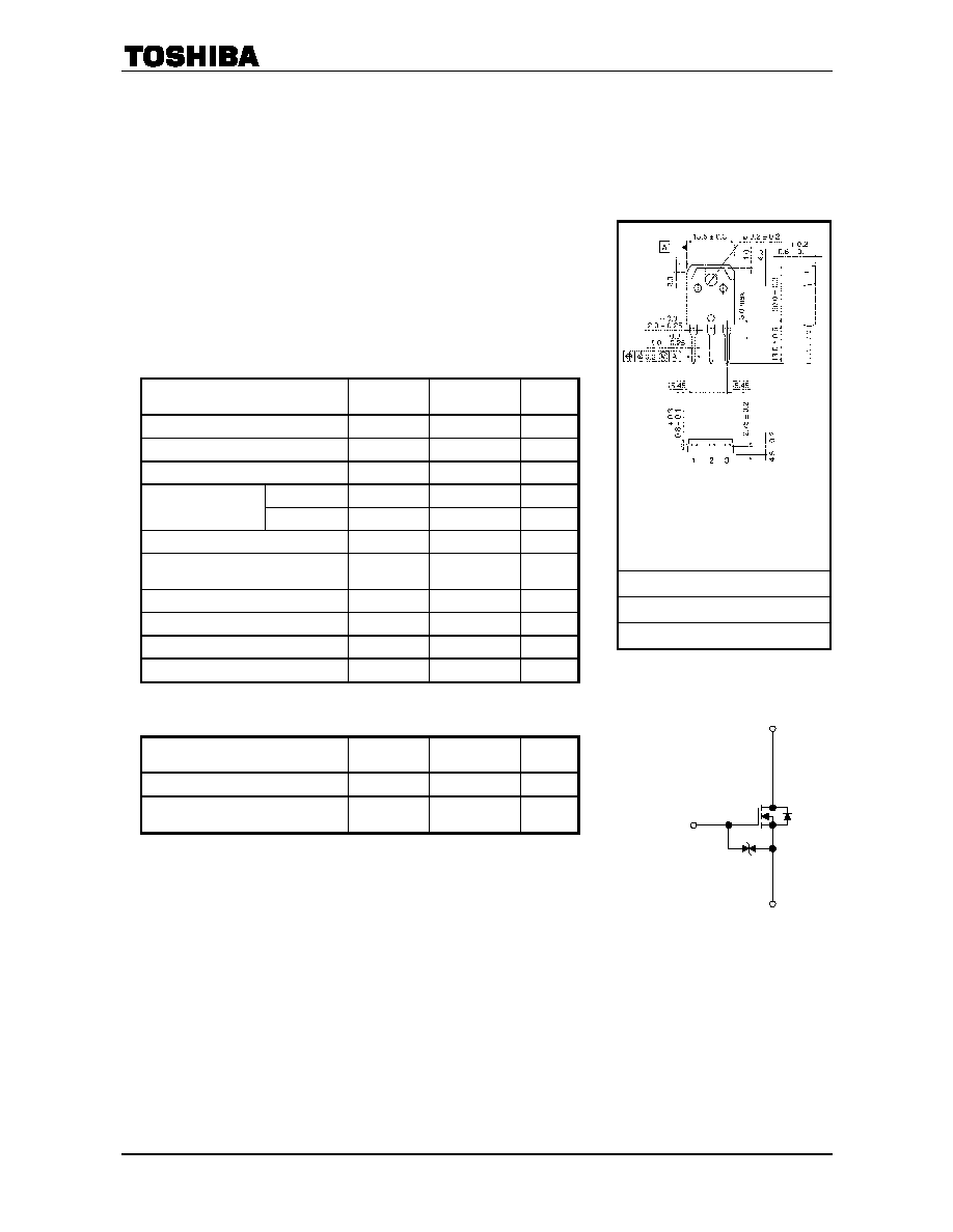
Unit: mm
1: GATE
2: DRAIN (HEAT SINK)
3: SOURCE
JEDEC
JEITA
TOSHIBA 2-16K1A
Weight: 3.8 g (typ.)
1
3
2
TK19H50C
2005-08-23
2
Electrical Characteristics
(Ta = 25∞C)
Characteristic Symbol
Test
Condition
Min
Typ.
Max
Unit
Gate leakage current
I
GSS
V
GS
= ±25 V, V
DS
= 0 V
--
--
±10
µA
Gate-source breakdown voltage
V
(BR) GSS
I
G
= ±10 µA, V
DS
= 0 V
±30
--
--
V
Drain cutoff current
I
DSS
V
DS
= 500 V, V
GS
= 0 V
--
--
100
µA
Drain-source breakdown voltage
V
(BR) DSS
I
D
= 10 mA, V
GS
= 0 V
500
--
--
V
Gate threshold voltage
V
th
V
DS
= 10 V, I
D
= 1 mA
2.0
--
4.0
V
Drain-source ON resistance
R
DS (ON)
V
GS
= 10 V, I
D
= 9.5 A
--
0.25
0.30
Forward transfer admittance
|Y
fs
| V
DS
= 10 V, I
D
= 9.5 A
4.0
14
--
S
Input capacitance
C
iss
--
3100
--
Reverse transfer capacitance
C
rss
--
20
--
Output capacitance
C
oss
V
DS
= 25 V, V
GS
= 0 V, f = 1 MHz
-- 270 --
pF
Rise time
t
r
--
70
--
Turn on time
t
on
-- 130 --
Fall time
t
f
--
70
--
Switching time
Turn off time
t
off
-- 280 --
ns
Total gate charge (gate-source
plus gate-drain)
Q
g
--
62
--
Gate-source charge
Q
gs
--
40
--
Gate-drain ("Miller") charge
Q
gd
V
DD
400 V, V
GS
= 10 V, I
D
= 19 A
-- 22 --
nC
Source-Drain Ratings and Characteristics
(Ta = 25∞C)
Characteristic Symbol
Test
Condition
Min
Typ.
Max
Unit
Continuous drain reverse current
(Note
1)
I
DR
--
--
--
19
A
Pulse drain reverse current
(Note
1)
I
DRP
--
--
--
76
A
Forward voltage (diode)
V
DSF
I
DR
= 19 A, V
GS
= 0 V
--
--
-1.7 V
Reverse recovery time
t
rr
-- 1200 -- ns
Reverse recovery charge
Q
rr
I
DR
= 19 A, V
GS
= 0 V
dI
DR
/ dt = 100 A / µs
-- 18 -- µC
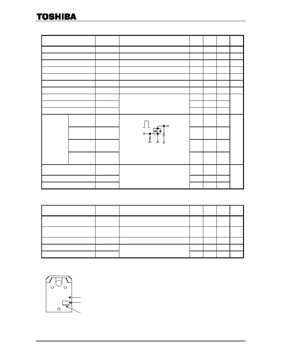
Marking
R
L
= 21
V
DD
- 200 V
0 V
V
GS
10 V
50
I
D
= 9.5A
Duty <= 1%, t
w
= 10 µs
TK19H50C
TOSHIBA
Lot No.
A line indicates a
lead (Pb)-free package or
lead (Pb)-free finish.
Part No. (or abbreviation code)
TK19H50C
2005-08-23
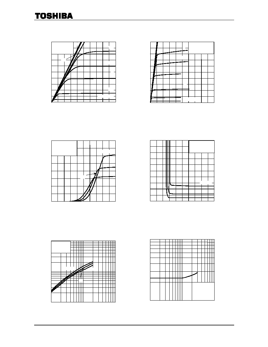
3
VGS = 4V
4.5
5
5.25
6
8
10
5.5
Common source
Tc
= 25∞C
Pulse Test
I
D
≠ V
DS
I
D
≠ V
DS
I
D
≠ V
GS
V
DS
≠ V
GS
20
30 40 50
0
8
12
16
20
4
0
10
8
12 16 20
0
8
12
16
20
4
0
4
0
2
4
6
8
10
2 3 4 5
0 1
4 8
0
40
60
80
20
0 2
10
6
VGS = 4 V
4.5
5
5.5
Common source
Tc
= 25∞C
Pulse Test
10
8
6
5.75
Common source
VDS = 10 V
Pulse Test
Tc
= -55∞C
100
25
|Y
fs
| ≠ I
D
10
100
1
10
100
1
Common source
VDS = 10 V
Pulse Test
Tc
= -55∞C
25
100
R
DS (ON)
≠ I
D
1
10
100
0.1
1.0
Common source
Tc
= 25∞C
VGS = 10 V
Pulse Test
Drain-source voltage VDS (V)
Drain
cu
r
r
e
n
t
I D
(A
)
Drain-source voltage VDS (V)
D
r
ain
cu
rre
nt
I
D
(
A
)
Gate-source voltage VGS (V)
D
r
a
i
n cur
r
ent
I D
(A
)
Gate-source voltage VGS (V)
Drain current ID (A)
Drain current ID (A)
D
r
a
i
n
-
so
urc
e
O
N
r
e
sis
t
anc
e
R
DS
(O
N
)
(
)
D
r
ain
-
so
urc
e
v
o
lt
a
ge
V
DS
(V
)
F
o
r
w
ar
d t
r
a
n
sfe
r
ad
mittan
c
e
Y
fs
(S
)
ID = 19 A
4
9.5
Common source
Tc
= 25∞C
Pulse Test
TK19H50C
2005-08-23
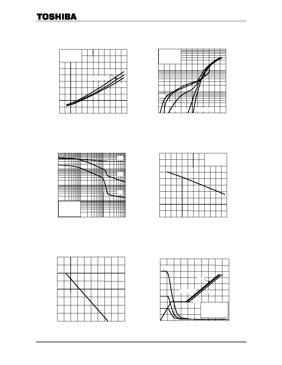
4
V
th
- Tc
R
DS (ON)
- Tc
0
1.0
0.2
0.6
0.4
-40
-80 160
0 40
120
80
I
DR
- V
DS
P
D
- Tc
200
50
100
150
0
0 80
40 160
120
0.8
1
100
0.1 100
1000
1 10
10000
0.2
0
0.4
0.6
1.2
0.1
1
100
10
Common source
Tc
= 25∞C
Pulse Test
VGS = 0 V
1
10
5
3
0.8 1.0
Ciss
Coss
Crss
Common source
VGS = 0 V
f
= 1 MHz
Tc
= 25∞C
0
-80
0
40
80 120 160
-40
1
2
3
4
5
Common source
VDS = 10 V
ID = 1mA
Pulse Test
200
10
Case temperature Tc (∞C)
Gate
th
res
h
ol
d vol
t
a
g
e
V
th
(V
)
Case temperature Tc (∞C)
Total gate charge Qg (nC)
C
apaci
t
anc
e
C
(p
F)
Capacitance ≠ V
DS
Drain-source voltage VDS (V)
D
r
ain
-
so
urc
e
O
N
r
e
sis
t
anc
e
R
DS
(O
N)
(
)
Case temperature Tc (∞C)
Drain
re
v
e
r
s
e c
u
r
r
e
n
t
I DR
(A
)
Drain-source voltage VDS (V)
D
r
a
i
n
po
wer
di
ssi
p
a
ti
on
P
D
(
W
)
D
r
ain
-
so
urc
e
v
o
lt
a
ge
V
DS
(V
)
Dynamic input / output
characteristics
G
a
te
-so
u
r
c
e v
o
ltage
V
GS
(V)
ID = 19A
9.5
4
Common source
VGS = 10 V
Pulse Test
500
0
300
200
0
40
60
20
0
20
80 100
VDD = 100V
200V
400V
VDS
VGS
Common source
ID = 19 A
Ta
= 25∞C
Pulse Test
400
100
4
8
12
16
TK19H50C
2005-08-23
5
-15 V
15
V
Test circuit
Wave form
I
AR
B
VDSS
V
DD
V
DS
R
G
= 25
V
DD
= 90 V, L = 4.56 mH
-
=
VDD
BVDSS
BVDSS
2
I
L
2
1
AS
r
th
- t
w
1000
1 10 100
0.001
10
100 1m 10m
100m
1 10
0.01
0.1
1
0.1
1
100
0.01
1000
10
10
E
AS
≠ T
ch
SINGLE PULSE
T
PDM
t
Duty
= t/T
Rth (ch-c) = 0.833∞C/W
Duty=0.5
0.2
0.1
0.05
0.02
0.01
Single pulse Ta=25
Curves must be derated
linearly with increase in
temperature.
ID max (pulse) *
ID max (continuous)
DC OPEATION
Tc
= 25∞C
100
µs *
1 ms *
VDSS max
Pulse width tw (s)
Nor
m
ali
z
ed t
r
a
n
sie
n
t t
h
e
r
m
a
l im
pe
da
nc
e
r
th (t
)
/R
th (c
h-
c
)
SAFE OPERATING AREA
Drain-source voltage VDS (V)
D
r
ain
cu
rre
nt I
D
(A)
Channel temperature (initial) T
ch
(∞C)
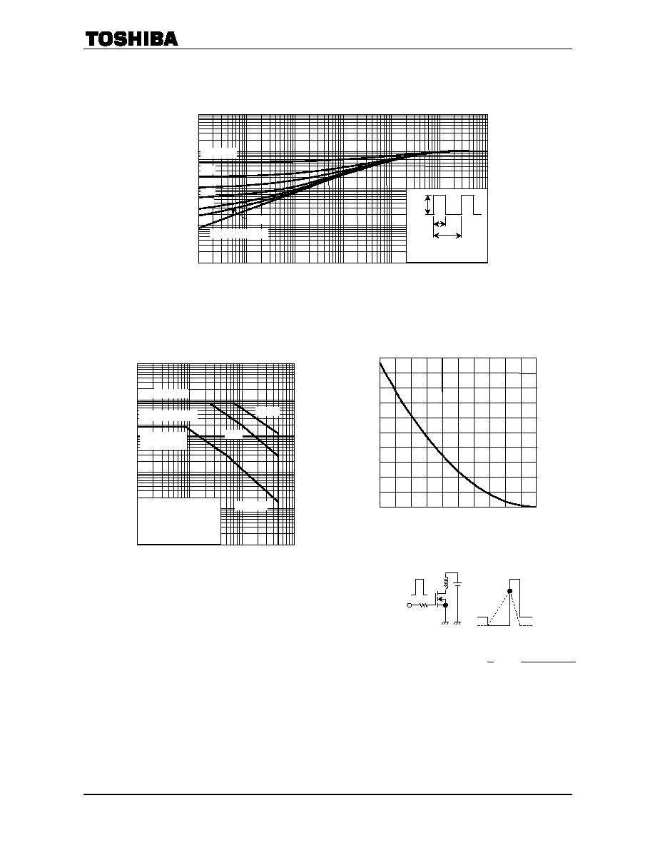
Av
a
l
a
n
c
he energ
y
E
AS
(
m
J
)
800
600
400
200
0
25 50 75 100 125 150
1000