 | –≠–ª–µ–∫—Ç—Ä–æ–Ω–Ω—ã–π –∫–æ–º–ø–æ–Ω–µ–Ω—Ç: TLP112 | –°–∫–∞—á–∞—Ç—å:  PDF PDF  ZIP ZIP |
TLP112
2002-09-25
1
TOSHIBA
Photocoupler
GaAAs Ired & Photo-IC
TLP112
Digital Logic Isolation
Line Receiver
Switching Power Supply Feedback Control
Transistor Invertor
The TOSHIBA mini flat coupler TLP112 is a small outline coupler,
suitable for surface mount assembly.
TLP112 consists of a GaAAs light emitting diode, optically coupled to a
high speed detector of one chip photodiode
-
transistor.
l Isolation voltage: 2500 Vrms (min.)
l Switching speed: t
pHL
= 0.8µs,
t
pLH
= 2 µs(max.)
(R
L
= 4.1 k)
l TTL compatible
l UL recognized: UL1577, file no. E67349
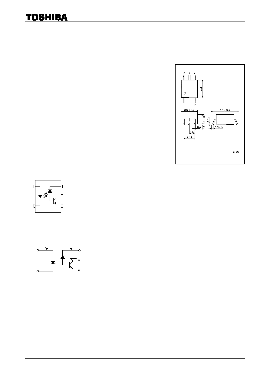
Pin Configuration
(top view)
1 : ANODE
3 : CATHODE
4 : EMITTER (GND)
5 : COLLECTOR (OUTPUT)
6 : V
CC
1
3
4
5
6
Schematic
V
CC
GND
V
O
I
CC
I
O
6
5
4
1
3
I
F
V
F
TOSHIBA 11-4C2
Weight: 0.09g
Unit in mm

TLP112
2002-09-25
2
Maximum Ratings
(Ta = 25∞C)
Characteristic Symbol
Rating
Unit
Forward current
(Note 1)
I
F
25 mA
Pulse forward current
(Note 2)
I
FP
50 mA
Peak transient forward
current (Note
3)
I
FPT
1 A
Reverse voltage
V
R
5 V
LE
D
Diode power dissipation
(Note 4)
P
D
45 mW
Output current
I
O
8 mA
Peak output current
I
OP
16 mA
Supply voltage
V
CC
-0.5~15 V
Output voltage
V
O
-0.5~15 V
Det
e
c
t
or
Output power dissipation
(Note 5)
P
o
100 mW
Operating temperature range
T
opr
-55~100 ∞C
Storage temperature range
T
stg
-55~125 ∞C
Lead soldering temperature(10s)
T
sol
260 ∞C
Isolation voltage
(AC, 1 min., R.H 60%,
Note 6)
BV
S
2500 Vrms
(Note 1) Derate 0.8 mA / ∞C above 70∞C.
(Note 2) 50% duty cycle,1ms pulse width.
Derate 1.6mA / ∞C above 70∞C.
(Note 3) Pulse width 1µs, 300pps.
(Note 4) Derate 0.9mW / ∞C above 70∞C.
(Note 5) Derate 2mW / ∞C above 70∞C.
TLP112
2002-09-25
3
Electrical Characteristics
(Ta = 25∞C)
Characteristic Symbol
Test
Condition
Min.
Typ.
Max.
Unit
Forward voltage
V
F
I
F
= 16mA
1.65 1.85
V
Forward voltage
temperature coefficient
V
F
/ Ta I
F
= 16mA
-2
mV / ∞C
Reverse current
I
R
V
R
= 5V
10 µA
LE
D
Capacitance between
terminals
C
T
V
F
= 0, f = 1MHz
45 pF
I
OH (1)
I
F
= 0mA, V
CC
= V
O
= 5.5V
3 500
nA
I
OH (2)
I
F
= 0mA, V
CC
= V
O
= 15V
5
High level output
current
I
OH
I
F
= 0mA, V
CC
= V
O
= 15V
Ta = 70∞C
50
µA
Det
e
c
t
or
High level supply
current
I
CCH
I
F
= 0mA, V
CC
= 15V
0.01 1 µA
Current transfer ratio
I
O
/ I
F
I
F
=16mA, V
CC
= 4.5V
V
O
= 0.4V
10
%
Low level output
voltage
V
OL
I
F
= 16 mA, V
CC
= 4.5V
I
O
= 1.1mA
0.4 V
Isolation resistance
R
S
R.H. 60%
V
S
= 500V DC
(Note 6)
5◊10
10
10
14
Coupl
ed
Stray capacitance
between input to output
C
S
V
S
= 0, f = 1MHz
(Note 6)
0.8 pF
Switching Characteristics
(Ta = 25∞C)
Characteristic Symbol
Test
Cir
-
cuit
Test Condition
Min.
Typ.
Max.
Unit
Propagation delay time
(HL)
t
pHL
1
I
F
= 016mA
V
CC
= 5V, R
L
= 4.1k
0.8 µs
Propagation delay time
(LH)
t
pLH
1
I
F
= 160mA
V
CC
= 5V, R
L
= 4.1k
2.0 µs
Common mode transient
immunity at high output
level
CM
H
2
I
F
= 0mA, V
CM
= 200V
p
-p
R
L
= 4.1k
1500 V
/
µs
Common mode transient
immunity at low output
level
CM
L
2
I
F
=16mA, V
CM
= 200V
p
-p
R
L
= 4.1k
-1500
V
/
µs
(Note 6) Device considered a two
-terminal device: Pins 1 and 3 shorted together and Pin 4,
5 and 6 shorted together.
(Note 7) Maximum electrostatic discharge voltage for any pins: 100V (C=200pF, R=0)
TLP112
2002-09-25
4
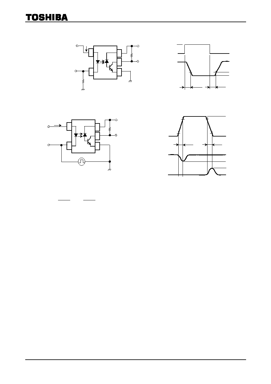
Test Circuit 1: Switching Time Test Circuit
Test Circuit 2: Common Mode Transient Immunity Test Circuit
µs
f
t
V
160
=
L
C
,
µs
r
t
V
160
=
H
C
V
O
I
F
5V
1.5V
0
V
OL
t
pLH
t
pHL
1.5V
PW = 100s
DUTY RATIO = 1 / 10
I
F
MONITOR
PULSE INPUT
OUTPUT
MONITOR
V
O
V
CC
= 5V
R
L
I
F
100
1
3
4
6
5
I
F
PULSE GENERATOR
Z
O
= 50
V
CM
OUTPUT
MONITOR
V
O
V
CC
= 5V
1
3
4
5
6
R
L
0V
V
O
V
CM
90%
5V
2V
0.8V
V
OL
t
r
t
f
10%
V
O
(I
F
= 16mA)
(I
F
= 0mA)
200V
TLP112
2002-09-25
5
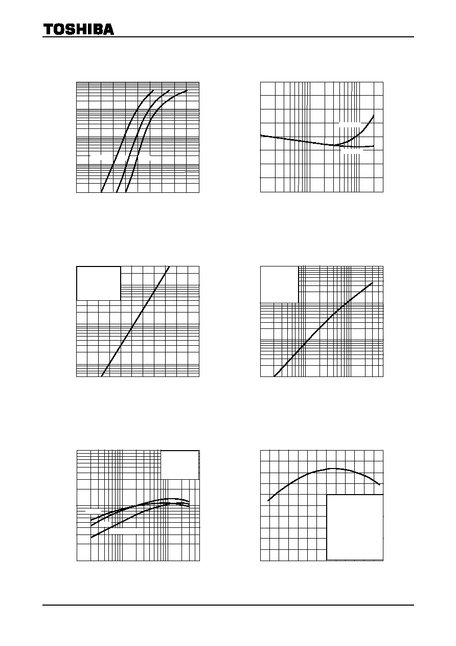
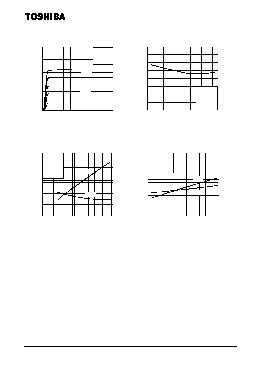
I
F
≠ V
F
Forward voltage V
F
(V)
Forward c
u
rrent
I
F
(m
A
)
100
1.0
10
1.2 1.4 1.6 1.8
2.0
1
0.1
0.01
Ta = 70∞C
25∞C
0∞C
V
F
/ Ta ≠ I
F
Foward current I
F
(mA)
Forward v
o
l
t
age
t
e
m
perat
ure
c
oef
f
i
c
i
ent
V
F
/
Ta
(
m
V
/
∞
C
)
-4.0
0.1
-3.2
-2.4
-1.6
0.3 0.5
1
3 5 10
-0.8
30
2570∞C
025∞C
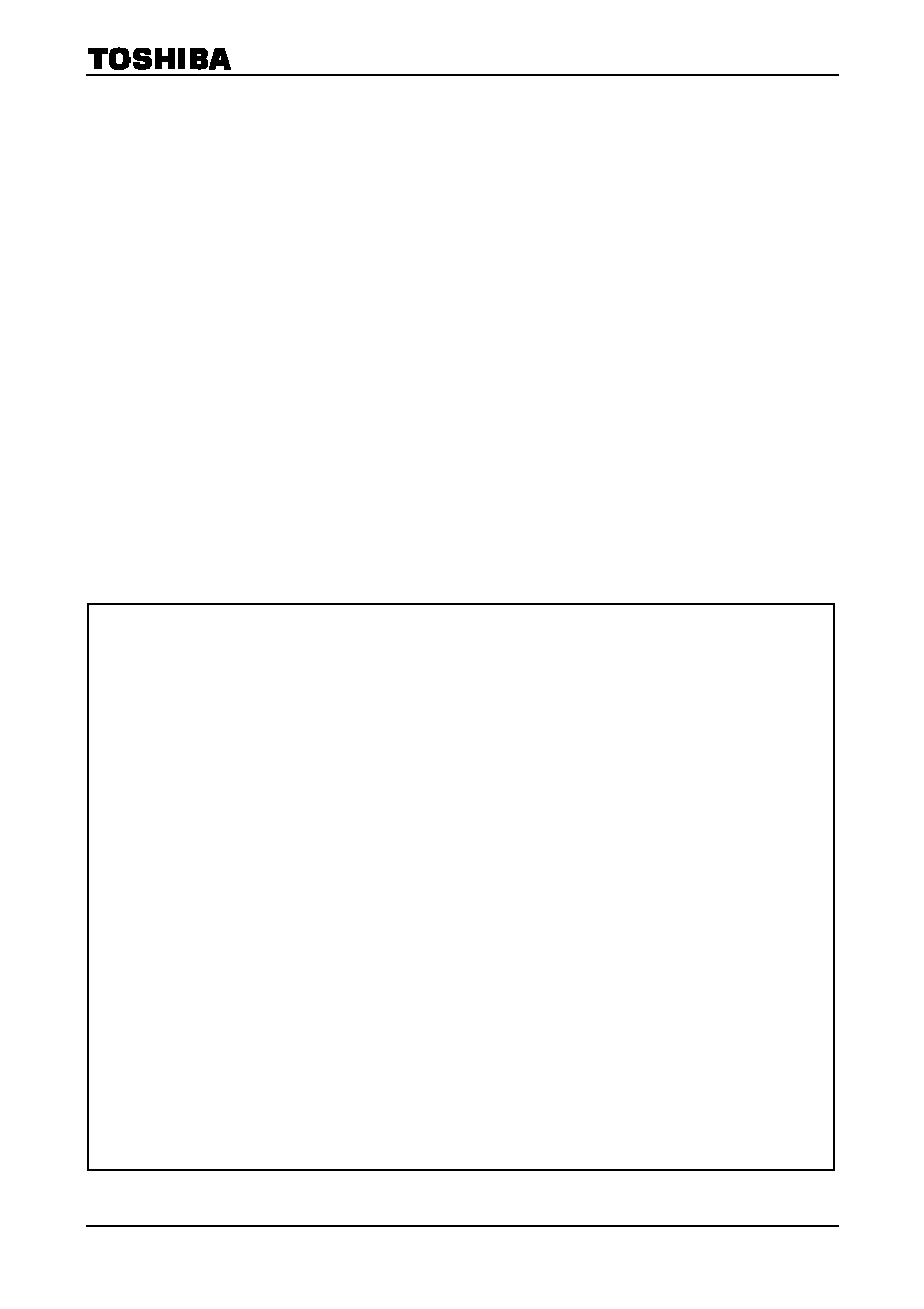
I
O
I
F
Forward current I
F
(mA)
Out
put
c
u
rrent
I
O
(m
A
)
10
0.01
3
0.3
0.03
50
30
10
5
3
1
0.5
0.3
0.1
0.1
1
VCC = 5V
VO = 0.4V
Ta = 25∞C
I
O
/ I
F
I
F
Forward current I
F
(mA)
Current
t
r
ans
f
e
r
rat
i
o
I
O
/
I
F
(%
)
50
30
10
5
3
1
0.5
0.3
100
50
30
10
5
3
1
VCC = 5V
VO = 0.4V
Ta = 100∞C
- 25∞C
25∞C
0.1
I
O
/ I
F
≠ Ta
Ambient temperature Ta (∞C)
N
o
r
m
a
liz
e
d
I
O /
I
F
0
20
40
60
80
-20
100
0.2
0.4
0.6
0.8
1.0
1.2
Normalized to
IF = 16mA
VCC = 4.5V
VO = 0.4V
Ta = 25∞C
I
OH(1)
≠ Ta
Ambient temperature Ta (∞C)
Hi
gh l
e
v
e
l
out
put
c
u
rrent
I
OH
(
A)
100
1
3
50
30
10
5
0
40
80
0.5
300
20
60
100
VF = 1V
VCC = 5.5V
VO = 5.5V
TLP112
2002-09-25
6
I
O
≠ V
O
Output voltage V
O
(V)
Out
put
c
u
rrent
I
O
(m
A
)
5
4
1
0
VCC = 5V
Ta = 25∞C
10mA
15mA
20mA
25mA
I
F
= 5mA
5
4
3
2
1
0
2
3
t
pHL,
t
pLH
≠ R
L
Load resistance R
L
(k)
P
r
op
agat
i
on del
a
y
t
i
m
e
t
pH
L,
t
pLH
(
s)
3
1
0.3
1
5
10
50
100
0.1
5
30
3
0.5
t
pLH
t
pHL
IF = 16mA
VCC = 5V
Ta = 25∞C
t
pHL,
t
pLH
≠ Ta
Ambient temperature Ta (∞C)
P
r
op
agat
i
on del
a
y
t
i
m
e
t
pH
L,
t
pLH
(
s)
3
1
0.3
0
40
80
100
0.1
60
20
0.5
t
pLH
t
pHL
IF = 16mA
VCC = 5V
R
L
= 4.1k
V
OL
≠ Ta
Ambient temperature Ta (∞C)
- 20
20
40
60 80
0
0.2
Low l
e
v
e
l
out
put
v
o
l
t
age
V
OL
(
V
)
0.4
0.3
0.1
100
0
IF = 16mA
VCC = 5V
IO = 1.1mA
TLP112
2002-09-25
7
∑ TOSHIBA is continually working to improve the quality and reliability of its products. Nevertheless, semiconductor
devices in general can malfunction or fail due to their inherent electrical sensitivity and vulnerability to physical
stress. It is the responsibility of the buyer, when utilizing TOSHIBA products, to comply with the standards of
safety in making a safe design for the entire system, and to avoid situations in which a malfunction or failure of
such TOSHIBA products could cause loss of human life, bodily injury or damage to property.
In developing your designs, please ensure that TOSHIBA products are used within specified operating ranges as
set forth in the most recent TOSHIBA products specifications. Also, please keep in mind the precautions and
conditions set forth in the "Handling Guide for Semiconductor Devices," or "TOSHIBA Semiconductor Reliability
Handbook" etc..
∑ The TOSHIBA products listed in this document are intended for usage in general electronics applications
(computer, personal equipment, office equipment, measuring equipment, industrial robotics, domestic appliances,
etc.). These TOSHIBA products are neither intended nor warranted for usage in equipment that requires
extraordinarily high quality and/or reliability or a malfunction or failure of which may cause loss of human life or
bodily injury ("Unintended Usage"). Unintended Usage include atomic energy control instruments, airplane or
spaceship instruments, transportation instruments, traffic signal instruments, combustion control instruments,
medical instruments, all types of safety devices, etc.. Unintended Usage of TOSHIBA products listed in this
document shall be made at the customer's own risk.
∑ Gallium arsenide (GaAs) is a substance used in the products described in this document. GaAs dust and fumes
are toxic. Do not break, cut or pulverize the product, or use chemicals to dissolve them. When disposing of the
products, follow the appropriate regulations. Do not dispose of the products with other industrial waste or with
domestic garbage.
∑ The products described in this document are subject to the foreign exchange and foreign trade laws.
∑ The information contained herein is presented only as a guide for the applications of our products. No
responsibility is assumed by TOSHIBA CORPORATION for any infringements of intellectual property or other
rights of the third parties which may result from its use. No license is granted by implication or otherwise under
any intellectual property or other rights of TOSHIBA CORPORATION or others.
∑ The information contained herein is subject to change without notice.
000707EBC
RESTRICTIONS ON PRODUCT USE