Электронный компонент:
TMP87C847U
Скачать:
PDF
ZIP
Document Outline
FEATURES
PIN ASSIGNMENTS (TOP VIEW)
BLOCK DIAGRAM
PIN FUNCTION
OPERATIONAL DESCRIPTION
1. CPU CORE FUNCTIONS
1.1 Memory Address Map
1.2 Program Memory (ROM)
1.3 Program Counter (PC)
1.4 Data Memory (RAM)
1.5 General-purpose Register Banks
1.6 Program Status Word (PSW)
1.6.1 Register Bank Selector (RBS)
1.6.2 Flags
1.7 Stack, Stack Pointer
1.7.1 Stack
1.7.2 Stack Pointer (SP)
1.8 System Clock Controller
1.8.1 Clock Generator
1.8.2 Timing Generator
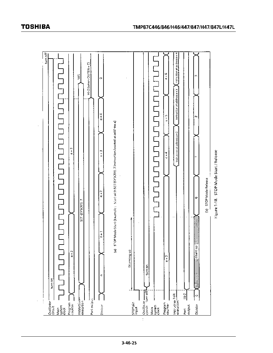
1.8.3 Stand-by Controller
1.8.4 Operaing Mode Control
1.9 Interrupt Controller
1.9.1 Interrupt Sequence
1.9.2 External Interrupts
1.9.3 Software Interrupt (INTSW)
1.10 Watchdog Timer (WDT)
1.10.1 Watchdog Timer Configuration
1.10.2 Watchdog Timer Control
1.10.3 Watchdog Timer Interrupt (INTWDT)
1.10.4 Watchdog Timer Reset
1.11 Reset Circuit
1.11.1 External Reset Input
1.11.2 Address-Trap-Reset
1.11.3 Watchdog Timer Reset
1.11.4 System Clock Reset
2. ON-CHIP PERIPHERALS FUNCTIONS
2.1 Special Function Registers (SFR) and Data Buffer Registers (DBR)
2.2 I/O Ports
2.2.1 Port P0 (P07 to P00)
2.2.2 Port P1 (P17 to P10)
2.2.3 Port P2 (P22 to P20)
2.2.4 Port P6 (P67 to P60)
2.2.5 Port P7 (P77 to P70)
2.2.6 Port P5 (P51 to P50)
2.3 Time Base Timer (TBT)
2.4 Divider Output (DVO)
2.5 16-bit Timer/Counter 1 (TC1)
2.5.1 Configuration
2.5.2 Control
2.5.3 Function
2.6 16-bit Timer/Counter 2 (TC2)
2.6.1 Configuration
2.6.2 Control
2.6.3 Function
2.7 8-Bit Timer/Counter 3 (TC3)
2.7.1 Configuration
2.7.2 Control
2.7.3 Function
2.8 8-Bit Timer/Counter 5 (TC5)
2.8.1 Configuration
2.8.2 Control
2.8.3 Function
2.9 Serial Interface (SIO)
2.9.1 Configuration
2.9.2 Control
2.9.3 Transfer Mode
2.10 8-bit High-speed Serial Output (HSO)
2.10.1 Configuration
2.10.2 Control
2.10.3 Transmit Operations
2.11 8-bit A/D Converter(ADC)
2.11.1 Configuration
2.11.2 Control
2.11.3 Operation
INPUT/OUTPUT CIRCUITRY
ELECTRICAL CHARACTERISTICS 87C446/846/H46/447/847/H47
ELECTRICAL CHARACTERISTICS 87C847L/H47L