 | –≠–ª–µ–∫—Ç—Ä–æ–Ω–Ω—ã–π –∫–æ–º–ø–æ–Ω–µ–Ω—Ç: TPC8111 | –°–∫–∞—á–∞—Ç—å:  PDF PDF  ZIP ZIP |

TPC8111
2002-03-25
1
TOSHIBA Field Effect Transistor Silicon P Channel MOS Type (U-MOS IV)
TPC8111
Lithium Ion Battery Applications
Notebook PC Applications
Portable Equipment Applications
∑ Small footprint due to small and thin package
∑ Low drain-source ON resistance: R
DS (ON)
= 8.1 m (typ.)
∑ High forward transfer admittance: |Y
fs
| = 23 S (typ.)
∑ Low leakage current: I
DSS
= -10 µA (max) (V
DS
= -30 V)
∑ Enhancement-mode: V
th
= -0.8 to -2.0 V (V
DS
= -10 V, I
D
= -1 mA)
Maximum Ratings
(Ta = 25∞C)
Characteristics Symbol
Rating
Unit
Drain-source voltage
V
DSS
-30 V
Drain-gate voltage (R
GS
= 20 k) V
DGR
-30 V
Gate-source voltage
V
GSS
±20 V
DC (Note
1)
I
D
-11
Drain current
Pulse (Note 1)
I
DP
-44
A
Drain power dissipation (t
= 10 s)
(Note
2a)
P
D
1.9
W
Drain power dissipation (t
= 10 s)
(Note
2b)
P
D
1.0
W
Single pulse avalanche energy
(Note
3)
E
AS
31.5
mJ
Avalanche current
I
AR
-11 A
Repetitive avalanche energy
(Note 2a) (Note 4)
E
AR
0.19
mJ
Channel temperature
T
ch
150
∞C
Storage temperature range
T
stg
-55 to 150
∞C
Note: For (Note 1), (Note 2), (Note 3) and (Note 4), please refer to the
next page.
This transistor is an electrostatic sensitive device. Please handle with
caution.
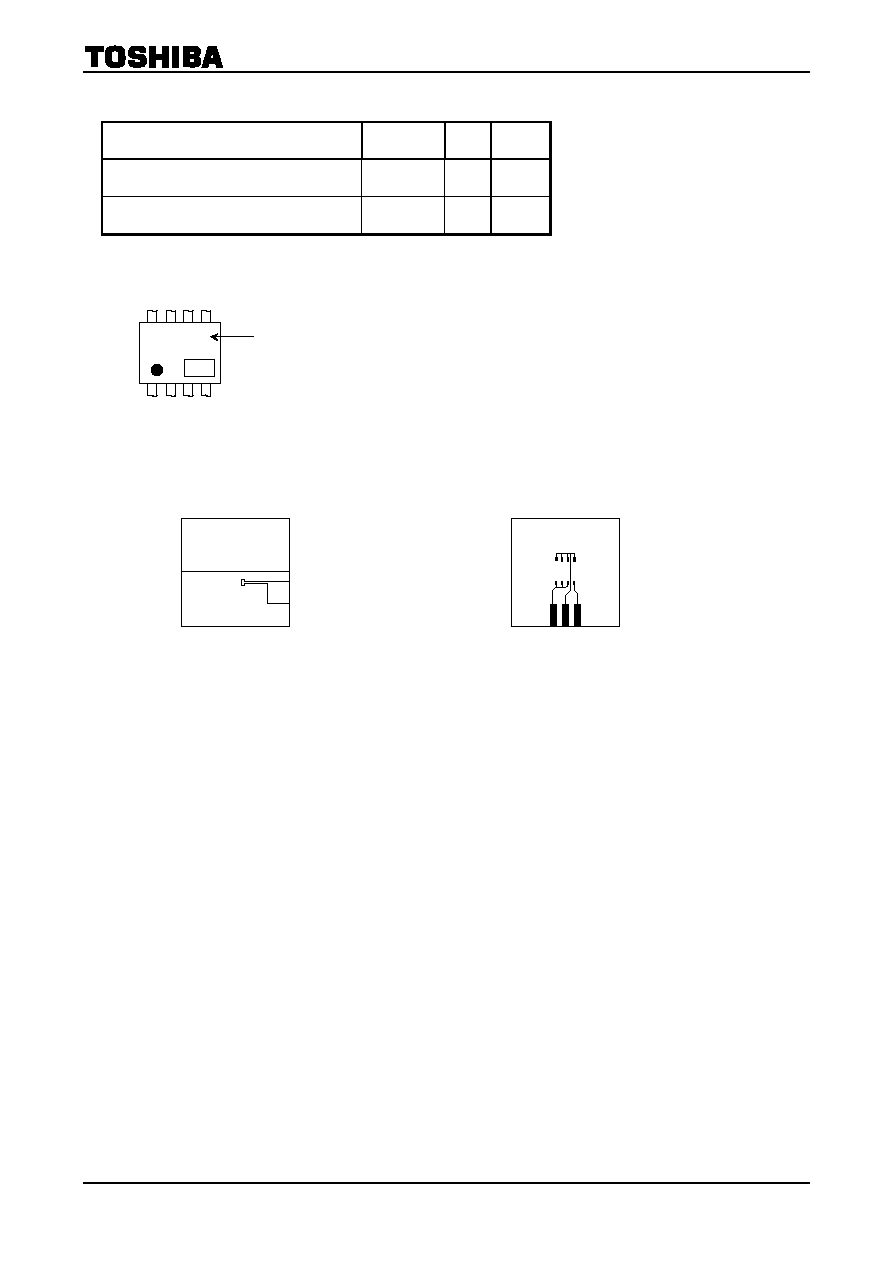
Unit: mm
JEDEC
JEITA
TOSHIBA 2-6J1B
Weight: 0.080 g (typ.)
Circuit Configuration
8 6
1 2 3
7
5
4
TPC8111
2002-03-25
2
Thermal Characteristics
Characteristics Symbol
Max
Unit
Thermal resistance, channel to ambient
(t
= 10 s)
(Note 2a)
R
th (ch-a)
65.8 ∞C/W
Thermal resistance, channel to ambient
(t
= 10 s)
(Note 2b)
R
th (ch-a)
125 ∞C/W
Marking
(Note 5)
Note 1: Please use devices on condition that the channel temperature is below 150∞C.
Note 2:
(a) Device mounted on a glass-epoxy board (a) (b) Device mounted on a glass-epoxy board (b)
Note 3: V
DD
= -24 V, T
ch
= 25∞C (initial), L = 0.2 mH, R
G
= 25 , I
AR
= -11 A
Note 4: Repetitive rating: pulse width limited by maximum channel temperature
Note 5:
∑ on lower left of the marking indicates Pin 1.
shows lot number. (year of manufacture: last decimal digit of the year of manufacture, month of
manufacture: January to December are denoted by letters A to L respectively.)
(b)
FR-4
25.4
◊ 25.4 ◊ 0.8
(unit:
mm)
(a)
FR-4
25.4
◊ 25.4 ◊ 0.8
(unit:
mm)
Type
TPC8111

TPC8111
2002-03-25
3
Electrical Characteristics
(Ta
=
=
=
=
25∞C)
Characteristics Symbol
Test
Condition
Min
Typ.
Max
Unit
Gate leakage current
I
GSS
V
GS
= ±16 V, V
DS
= 0 V
±10
µA
Drain cut-OFF current
I
DSS
V
DS
= -30 V, V
GS
= 0 V
-10
µA
V
(BR) DSS
I
D
= -10 mA, V
GS
= 0 V
-30
Drain-source breakdown voltage
V
(BR) DSX
I
D
= -10 mA, V
GS
= 20 V
-15
V
Gate threshold voltage
V
th
V
DS
= -10 V, I
D
= -1 mA
-0.8
-2.0 V
V
GS
= -4 V, I
D
= -5.5 A
12 18
Drain-source ON resistance
R
DS (ON)
V
GS
= -10 V, I
D
= -5.5 A
8.1 12
m
Forward transfer admittance
|Y
fs
| V
DS
= -10 V, I
D
= -5.5 A
11 23
S
Input capacitance
C
iss
5710
Reverse transfer capacitance
C
rss
560
Output capacitance
C
oss
V
DS
= -10 V, V
GS
= 0 V, f = 1 MHz
590
pF
Rise time
t
r
18
Turn-ON time
t
on
23
Fall time
t
f
109
Switching time
Turn-OFF time
t
off
Duty <
= 1%, t
w
= 10 µs
396
ns
Total gate charge
(gate-source plus gate-drain)
Q
g
107
Gate-source charge 1
Q
gs1
12
Gate-drain ("miller") charge
Q
gd
V
DD
- -24 V, V
GS
= 10 V,
I
D
= -11 A
20
nC
Source-Drain Ratings and Characteristics
(Ta
=
=
=
=
25∞C)
Characteristics Symbol
Test
Condition
Min
Typ.
Max
Unit
Drain reverse current
Pulse
(Note 1)
I
DRP
-44 A
Forward voltage (diode)
V
DSF
I
DR
= -11 A, V
GS
= 0 V
1.2 V
R
L
=
2.
7
V
DD
- -15 V
0 V
V
GS
-10 V
4.
7
I
D
= -5.5 A
V
OUT

TPC8111
2002-03-25
4
Fo
r
w
ar
d t
r
a
n
sfe
r
adm
i
tta
nce
|Y
fs
|
(S
)
D
r
ai
n
-
so
urc
e
v
o
l
t
a
ge V
DS
(V
)
Drain-source voltage V
DS
(V)
I
D
≠ V
DS
D
r
ai
n
cu
rre
nt
I
D
(A
)
Drain-source voltage V
DS
(V)
I
D
≠ V
DS
D
r
ai
n
cu
rre
nt
I
D
(A
)
Gate-source voltage V
GS
(V)
I
D
≠ V
GS
D
r
ai
n
cu
rre
nt
I
D
(A
)
Gate-source voltage V
GS
(V)
V
DS
≠ V
GS
Drain current I
D
(A)
|Y
fs
| ≠ I
D
Drain current I
D
(A)
D
r
ai
n
-
so
urc
e
O
N
r
e
si
st
anc
e
R
DS (ON)
(m
)
R
DS (ON)
≠ I
D
-2
-3
-4
-5
Common source
VDS = -10 V
Pulse test
0
-20
-30
-40
-10
0
-1
100
Ta
= -55∞C
25
0
-2
0
-4
-6
-8
-10
-2
-4
-6
-8
-10
Common source
Ta
= 25∞C
Pulse test
VGS = -2 V
-2.2
-3
-10
-5
-4
-2.1
-2.3
-2.4
-2.5
-8
-12
-16
-20
Common source
Ta
= 25∞C
Pulse test
-2.2
VGS = -2.1 V
0
-8
-12
-16
-20
-4
0
-4
-3
-5
-4
-10
-2.3
-2.4
-2.5
-2.7
-2.6
-8
-12
-16
-20
Common source
Ta
= 25∞C
Pulse test
0
-0.2
-0.3
-0.4
-0.5
-0.1
0
-4
ID = -11 A
-2.5
-5.5
0.3
1
10
100
0.5
3
5
30
50
-0.1
-1
-10
-50
Common source
VDS = -10 V
Pulse test
Ta
= -55∞C
100
25
-30
-3 -5
-0.3 -0.5
0.3
1
10
100
0.5
3
5
30
50
-0.1
-1
-10
-50
Common source
Ta
= 25∞C
Pulse test
-30
-3 -5
-0.3 -0.5
-10
VGS = -4.5 V

TPC8111
2002-03-25
5
Ambient temperature Ta (∞C)
R
DS (ON)
≠ Ta
D
r
ai
n
-
so
urc
e
O
N
r
e
si
st
anc
e
R
DS (ON)
(m
)
Drain-source voltage V
DS
(V)
I
DR
≠ V
DS
D
r
ai
n
re
ver
s
e c
u
r
r
e
n
t
I
DR
(A
)
Drain-source voltage V
DS
(V)
Capacitance ≠ V
DS
C
apa
ci
ta
nce
C
(
p
F)
Ambient temperature Ta (∞C)
V
th
≠ Ta
Gate
th
res
hol
d vol
t
ag
e
V
th
(V
)
Ambient temperature Ta (∞C)
P
D
≠ Ta
D
r
ai
n
po
w
e
r
di
ssi
pati
on
P
D
(
W
)
Gate
-so
u
r
c
e v
o
l
t
a
ge
V
GS
(V
)
Total gate charge Q
g
(nC)
Dynamic Input/Output Characteristics
D
r
ai
n
-
so
urc
e
v
o
l
t
a
ge V
DS
(V
)
0
-0.1
-1
-10
-100
0.2 0.4 0.6 0.8 1
-10
Common source
Ta
= 25∞C
Pulse test
-5
-3
-1
VGS = 0 V
-1.5
0
-80
-40 0 40
120
160
80
-0.5
-1
-2
-2.5
Common source
VDS = -10 V
ID = -1 mA
Pulse test
100 150
175
0
0.8
1.2
1.6
2.0
0.4
0 50
(1) Device mounted on a
glass-epoxy board (a)
(Note 2a)
(2) Device mounted on a
glass-epoxy board (b)
(Note 2b)
t
= 10 s
(1)
(2)
25 75 125
15
0
-80
-40 0 40
120
160
80
5
10
20
25
VGS = -4.5 V
Common source
Pulse test
-10
ID = -11 A, -5.5 A, -2.5 A
ID = -11 A, -5.5 A, -2.5 A
100
-0.1
-1
-10
1000
10000
Coss
Ciss
Common source
VGS = 0 V
f
= 1 MHz
Ta
= 25∞C
Crss
30000
50000
3000
5000
300
500
-100
-0.3
-3
-30
-12
-8
0
-4
-10
-6
-2
0
-10
-20
-30
0 20
40 60 80
Common source
ID = -11 A
Ta
= 25∞C
Pulse test
VDD = -24 V
VDS
VGS
-6
-12
140
VDD = -24 V
-12
-6
-5
-15
-25
100 120