TPD1032F
2000-03-07 1/5
Toshiba Intelligent Power Device Silicon Monolithic Power MOS Integrated Circuit
T P D 1 0 3 2 F
2-IN-1 Low-Side Power Switch for Motor, Solenoid and Lamp Drivers
TPD1032F is a 2-IN-1 low-side switch.
The IC has a vertical MOSFET output which can be directly
driven from a CMOS or TTL logic circuit (e.g., an MPU). The IC
offers intelligent self-protection functions.
Features
∑ Built-in two power IC chips with a new structure combining a
control block and a vertical power MOSFET (L
2
--MOS) on
each chip.
∑ Can directly drive a power load from a CMOS or TTL logic.
∑ Built-in protection circuits against overvoltage (active clamp), overtemperature (thermal shutdown), and
overcurrent (current limiter).
∑ Low Drain-Source ON-resistance: R
DS (ON)
= 0.4 (max) (@V
IN
= 5 V, I
D
= 1 A, T
ch
= 25∞C)
∑ Low Leakage Current: I
DSS
= 10 µA (max) (@V
IN
= 0 V, V
DS
= 30 V, T
ch
= 25∞C)
∑ Low Input Current: I
IN
= 300 µA (max) (@V
IN
= 5 V, T
ch
= 25∞C)
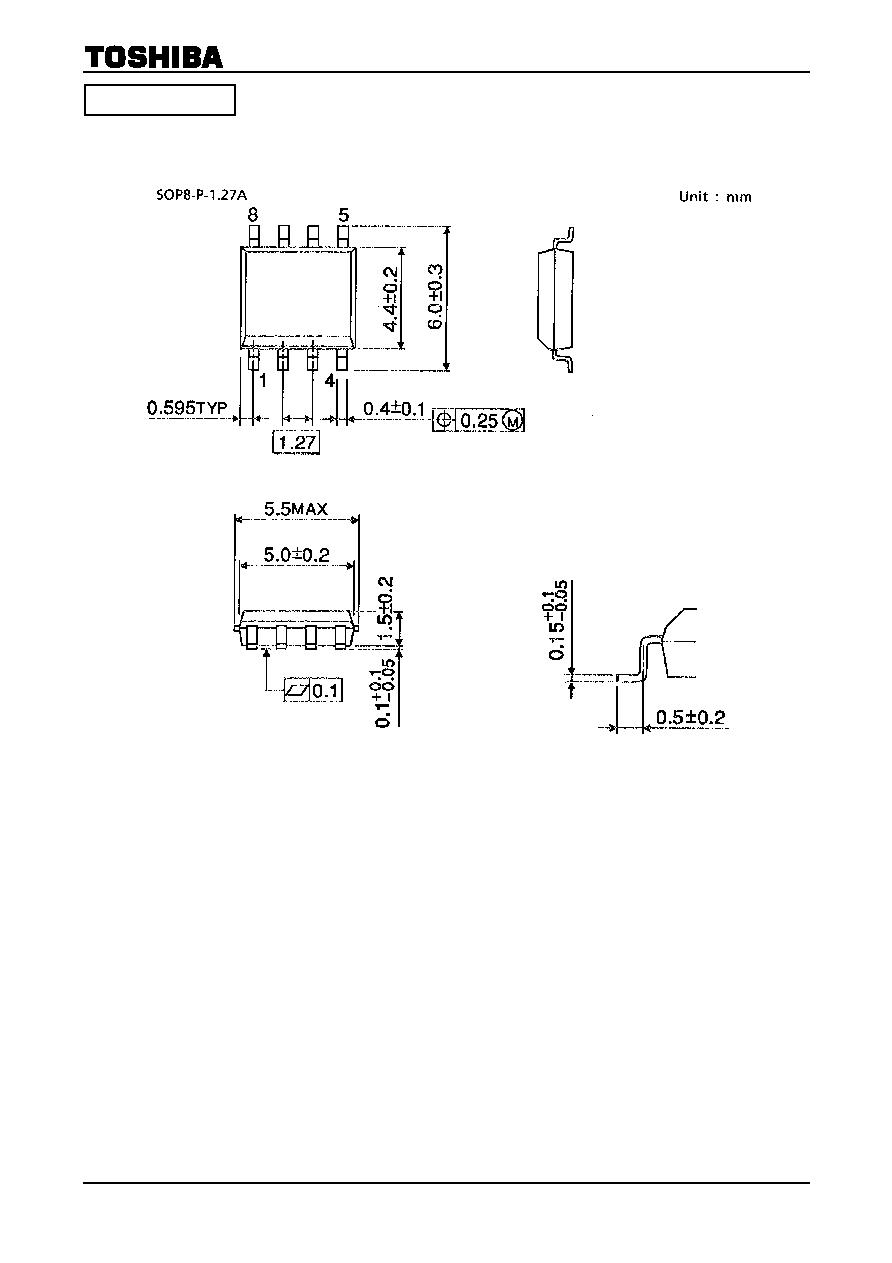
∑ 8-pin SOP package for surface with embossed-tape packing.
Pin Assignment
(top view)
Note1: That because of its MOS structure, this product is sensitive to static electricity.
Weight: 0.08 g (typ.)
Preliminary
∑ TOSHIBA is continually working to improve the quality and the reliability of its products. Nevertheless, semiconductor devices in
general can malfunction or fail due to their inherent electrical sensitivity and vulnerability to physical stress. It is the responsibility of
the buyer, when utilizing TOSHIBA products, to observe standards of safety, and to avoid situations in which a malfunction or failure
of a TOSHIBA product could cause loss of human life, bodily injury or damage to property. In developing your designs, please
ensure that TOSHIBA products are used within specified operating ranges as set forth in the most recent products specifications.
Also, please keep in mind the precautions and conditions set forth in the TOSHIBA Semiconductor Reliability Handbook.
∑ The products described in this document are subject to the foreign exchange and foreign trade laws.
∑ The information contained herein is presented only as a guide for the applications of our products. No responsibility is assumed by
TOSHIBA CORPORATION for any infringements of intellectual property or other rights of the third parties which may result from its
use. No license is granted by implication or otherwise under any intellectual property or other rights of TOSHIBA CORPORATION or
others.
∑ The information contained herein is subject to change without notice.
980910EBA1
SOURCE1
IN1
SOURCE2
1
2
3
8
6
7
DRAIN1
DRAIN1
DRAIN2
IN2 4
5 DRAIN2

TPD1032F
2000-03-07 2/5
Block Diagram
Pin Description
Pin No.
Symbol
Pin Description
1
SOURCE1
Source pin 1
2 IN1
Input pin 1
This pin is connected to a pull-down resistor internally, so that even when input wiring is
open-circuited, output can never be turned on inadvertently.
3
SOURCE2
Source pin 2
4 IN2
Input pin 2
This pin is connected to a pull-down resistor internally, so that even when input wiring is
open-circuited, output can never be turned on inadvertently.
5, 6
DRAIN2
Drain pin 2
Drain current is limited (by current limiter) if it exceeds 3 A (min) in order to protect the IC.
7, 8
DRAIN1
Drain pin 1
Drain current is limited (by current limiter) if it exceeds 3 A (min) in order to protect the IC.
DRAIN1
IN1
Overcurrent Detection
/Protection
8
7
Overtemperature Detection
/Protection
1
2
SOURCE1
DRAIN1
DRAIN2
IN2
Overcurrent Detection
/Protection
6
5
Overtemperature Detection
/Protection
3
4
SOURCE2
DRAIN2
Preliminary
TPD1032F
2000-03-07 3/5
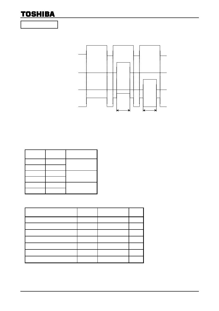
Timing Chart
Note2: The overheating detector circuits feature hysteresis. After overheating is detected, normal operation is
restored only when the channel temperature falls by the hysteresis amount (5∞C typ.) in relation to the
overheating detection temperature.
Truth Table
IN V
OUT
Mode
L H
H L
Normal
L H
H H
Overcurrent
L H
H H
Overtemperature
Maximum Ratings
(Ta
=
=
=
= 25∞C)
Characteristics Symbol
Rating
Unit
Drain-source voltage
V
DS (DC)
20 V
Drain current
I
D
Internally
Limited
A
Input voltage
V
IN
-0.3 to 7
V
Power dissipation (t
= 10 s)
P
D
2.0
(Note3)
W
Operating temperature
T
opr
-40 to 110
∞C
Channel temperature
T
ch
150
∞C
Storage temperature
T
stg
-55 to 150
∞C
Note3: Drive operation: Mount on glass epoxy boad [1 inch
2
◊ 0.8 t] (in the two devices driving)
Overcurrent Protection
Input Signal
Output Current
Current limiting
(limiter)
Overtemperature
protection (Note2)
Overtemperature Protection
Preliminary

TPD1032F
2000-03-07 4/5
Thermal Characteristics
Characteristics Symbol
Max
Unit
Thermal resistance, channel to
ambient (t
= 10 s)
(Note3)
R
th (ch-a)
62.5
∞C/W
Note3: Drive operation: Mount on glass epoxy boad [1 inch
2
◊ 0.8 t] (in the two devices driving)
Electrical Characteristics
(T
ch
=
=
=
= 25∞C)
Characteristics Symbol
Test
Circuit
Test Condition
Min
Typ.
Max
Unit
Drain-source clamp voltage
V
(CL) DSS
V
IN
= 0 V, I
D
= 1 mA
40
60 V
Input threshold voltage
V
th
V
DS
= 13 V, I
D
= 10 mA
1.0
2.8 V
Protective circuit operation input
voltage range
V
IN (opr)
3
7 V
Draint cut-off current
I
DSS
V
IN
= 0 V, V
DS
= 30 V
10 µA
I
IN (1)
V
IN
= 5 V, at normal operation
300
Input current
I
IN (2)
V
IN
= 5 V, when protective
circuit is actuated
390
µA
Drain-source on resistance
R
DS (ON)
V
IN
= 5 V, I
D
= 1 A
0.25 0.4
Overtemperature protection
T
S
V
IN
= 5 V
150
160
∞C
Overcurrent protection
I
S
V
IN
= 5 V
3
A
t
ON
1
30
Switching time
t
OFF
1
V
DD
= 13 V, V
IN
= 5 V,
I
D
= 1 A
60
µs
Source-drain diode forward voltage
V
DSF
I
F
= 3 A, V
IN
= 0 V
1.7 V
Test Circuit 1
Switching time measuring circuit
Test Circuit
Measured Waveforms
V
IN
Waveform
V
OUT
Waveform
5 V
90%
t
ON
10%
10%
90%
t
OFF
13 V
To be set so that
I
D
= 1 A.
V
13 V
P.G
TPD1032F
IN
OUT GND
Preliminary